

Page 1
SA58670A
2.1 W/channel stereo class-D audio amplifier
Rev. 02 — 23 October 2008 Product data sheet
1. General description
The SA58670A is a stereo, filter-free class-D audio amplifier which is available in an
HVQFN20 package with the exposed Die Attach Paddle (DAP).
The SA58670A features independent shutdown controls for each channel. The gain may
be set at 6 dB, 12 dB, 18 dB or 24 dB with gain select pins G0 and G1. Improved immunity
to noise and RF rectification is increased by high PSRR and differential circuit topology.
Fast start-up time and small package makes it an ideal choice for both cellular handsets
and PDAs.
The SA58670A delivers 1.4 W/channel at 5.0 V and 720 mW/channel at 3.6 V into 8 Ω. It
delivers 2.1 W/channel at 5.0 V into 4 Ω. The maximum power efficiency is excellent at
70 % to 74 % into 4 Ω and 84 % to 88 % into 8 Ω. The SA58670A provides thermal and
short-circuit shutdown protection.
2. Features
n Output power:
n Supply voltage: 2.5 V to 5.5 V
n Independent shutdown control for each channel
n Selectable gain: 6 dB, 12 dB, 18 dB and 24 dB
n High SVRR: −77 dB at 217 Hz
n Fast start-up time: 3.5 ms
n Low supply current
n Low shutdown current
n Short-circuit and thermal protection
n Space savings with 4 mm × 4 mm HVQFN20 package
n Low junction to ambient thermal resistance of 24 K/W with exposed DAP
3. Applications
n Wireless and cellular handset and PDA
n Portable DVD player
n USB speaker
n Notebook PC
n Portable radio and gaming
u 2.1 W/channel into 4 Ω at 5.0 V
u 1.4 W/channel into 8 Ω at 5.0 V
u 720 mW/channel into 8 Ω at 3.6 V
Page 2

NXP Semiconductors
n Educational toy
4. Ordering information
Table 1. Ordering information
Type number Package
SA58670ABS HVQFN20 plastic thermal enhanced very thin quad flat package;
5. Block diagram
SA58670A
2.1 W/channel stereo class-D audio amplifier
Name Description Version
SOT917-1
no leads; 20 terminals; body 4 × 4 × 0.85 mm
right input
left input
INRP
INRN
n.c.
INLP
INLN
G0
G1
SDR
SDL
Refer to Table 6 for gain selection.
Fig 1. Block diagram
SA58670A
16
17
6, 10
20
19
15
1
8
300 kΩ
7
300 kΩ
GAIN
ADJUST
GAIN
ADJUST
BIAS
CIRCUITRY
PWM
INTERNAL
OSCILLATOR
PWM
SHORT-CIRCUIT
PROTECTION
H-
BRIDGE
H-
BRIDGE
3, 13 PVDD
1411OUTRP
GND
2
5
9 AVDD
4, 12
18
002aad663
OUTRN
OUTLP
OUTLN
PGND
AGND
V
DD
V
DD
SA58670A_2 © NXP B.V. 2008. All rights reserved.
Product data sheet Rev. 02 — 23 October 2008 2 of 24
Page 3
NXP Semiconductors
6. Pinning information
6.1 Pinning
SA58670A
2.1 W/channel stereo class-D audio amplifier
terminal 1
index area
G1 G0
OUTLP OUTRP
PVDD PVDD
PGND
OUTLN
(1) Exposed Die Attach Paddle (DAP).
INLP
INLN
AGND
INRN
2019181716
115
214
313
SA58670ABS
412
(1)
DAP
511
6
7
8
9
n.c.
SDL
SDR
Transparent top view
AVDD
Fig 2. Pin configuration for HVQFN20
6.2 Pin description
Table 2. Pin description
Symbol Pin Description
G1 1 gain select input 1
OUTLP 2 left channel positive output
PVDD 3 power supply voltage (level same as AVDD)
PGND 4 power ground
OUTLN 5 left channel negative output
n.c. 6 not connected
SDL 7 left channel shutdown input (active LOW)
SDR 8 right channel shutdown input (active LOW)
AVDD 9 analog supply voltage (level same as PVDD)
n.c. 10 not connected
OUTRN 11 right channel negative output
PGND 12 power ground
PVDD 13 power supply voltage (level same as AVDD)
OUTRP 14 right channel positive output
G0 15 gain select input 0
INRP 16 right channel positive input
INRN 17 right channel negative input
AGND 18 analog ground
INRP
10
n.c.
PGND
OUTRN
002aad664
SA58670A_2 © NXP B.V. 2008. All rights reserved.
Product data sheet Rev. 02 — 23 October 2008 3 of 24
Page 4
NXP Semiconductors
SA58670A
2.1 W/channel stereo class-D audio amplifier
Table 2. Pin description
Symbol Pin Description
INLN 19 left channel negative input
INLP 20 left channel positive input
- (DAP) exposed die attach paddle; connect to ground plane heat spreader
7. Limiting values
Table 3. Limiting values
In accordance with the Absolute Maximum Rating System (IEC 60134).
Symbol Parameter Conditions Min Max Unit
V
DD
V
I
P power dissipation derating factor 41.6 mW/K
T
amb
T
j
T
stg
V
esd
…continued
[1]
supply voltage Active mode −0.3 +6.0 V
Shutdown mode −0.3 +7.0 V
input voltage pin SDL GND V
SDR GND V
pin
other pins −0.3 V
=25°C - 5.2 W
T
amb
=75°C - 3.12 W
T
amb
=85°C - 2.7 W
T
amb
DD
DD
DD
V
V
+ 0.3 V
ambient temperature operating in free air −40 +85 °C
junction temperature operating −40 +150 °C
storage temperature −65 +85 °C
electrostatic discharge
voltage
human body model ±2000 - V
machine model ±200 - V
[1] VDD is the supply voltage on pins PVDD and pin AVDD.
GND is the voltage ground on pins PGND and pin AGND.
SA58670A_2 © NXP B.V. 2008. All rights reserved.
Product data sheet Rev. 02 — 23 October 2008 4 of 24
Page 5
NXP Semiconductors
8. Static characteristics
SA58670A
2.1 W/channel stereo class-D audio amplifier
Table 4. Static characteristics
T
=25°C; unless otherwise specified
amb
[1]
.
Symbol Parameter Conditions Min Typ Max Unit
V
DD
I
DD
I
DD(sd)
PSRR power supply rejection ratio V
V
i(cm)
CMRR common mode rejection ratio inputs are shorted together;
V
IH
V
IL
I
IH
I
IL
f
sw
G
v(cl)
supply voltage operating 2.5 - 5.5 V
supply current VDD= 2.5 V; no load - 4 6 mA
= 3.6 V; no load - 5 7.5 mA
V
DD
= 5.5 V; no load - 6 9 mA
V
DD
shutdown mode supply current no input signal;
V
SDR=VSDL
= 2.5 V to 5.5 V - −75 −55 dB
DD
= GND
- 10 1000 nA
common-mode input voltage 0.5 - VDD− 0.8 V
- −69 −50 dB
= 2.5 V to 5.5 V
V
DD
HIGH-level input voltage VDD= 2.5 V to 5.5 V;
pins
SDL, SDR, G0, G1
LOW-level input voltage VDD= 2.5 V to 5.5 V;
pins
SDL, SDR, G0, G1
HIGH-level input current VDD= 5.5 V; VI=V
DD
1.3 - V
DD
0 - 0.35 V
--50 µA
V
LOW-level input current VDD= 5.5 V; VI=0V --5 µA
switching frequency VDD= 2.5 V to 5.5 V 250 300 350 kHz
closed-loop voltage gain VG0 = VG1 = 0.35 V 5.5 6 6.5 dB
= VDD; VG1 = 0.35 V 11.5 12 12.5 dB
V
G0
= 0.35 V; VG1 = V
V
G0
= VG1 = V
V
G0
DD
DD
17.5 18 18.5 dB
23.5 24 24.5 dB
Pins OUTLP, OUTLN, OUTRP and OUTRN
R
DSon
|V
O(offset)
Z
o(sd)
drain-source on-state resistance VDD= 2.5 V - 700 - mΩ
= 3.6 V - 570 - mΩ
V
DD
= 5.5 V - 500 - mΩ
V
DD
| output offset voltage measureddifferentially;inputs
shutdown mode output impedance V
AC grounded; G
V
= 2.5 V to 5.5 V
DD
= V
SDR
= 0.35 V - 2 - kΩ
SDL
v(cl)
= 6 dB;
- 5 10 mV
[1] VDD is the supply voltage on pins PVDD and pin AVDD.
GND is the ground supply voltage on pins PGND and pin AGND.
SA58670A_2 © NXP B.V. 2008. All rights reserved.
Product data sheet Rev. 02 — 23 October 2008 5 of 24
Page 6

NXP Semiconductors
9. Dynamic characteristics
SA58670A
2.1 W/channel stereo class-D audio amplifier
Table 5. Dynamic characteristics
T
=25°C; RL=8Ω; unless otherwise specified
amb
[1]
.
Symbol Parameter Conditions Min Typ Max Unit
P
o
THD+N total harmonic
SVRR supply voltage ripple
CMRR common mode rejection
output power per channel; f = 1 kHz; THD+N = 10 %
=8Ω; VDD= 3.6 V - 0.72 - W
R
L
=8Ω; VDD= 5.0 V - 1.4 - W
R
L
=4Ω; VDD= 5.0 V - 2.1 - W
R
L
distortion-plus-noise
rejection
= 5.0 V; G
V
DD
= 0.5 W - 0.11 - %
P
o
= 1.0 W - 0.14 - %
P
o
= 6 dB; f = 217 Hz
G
v(cl)
= 3.6 V - −73 - dB
V
DD
= 5.0 V - −77 - dB
V
DD
= 5.0 V; G
V
DD
= 6 dB; f=1kHz
v(cl)
= 6 dB; f = 217 Hz - −69 - dB
v(cl)
ratio
Z
i
t
d(sd-startup)
input impedance G
delay time from
= 6 dB - 28.1 - kΩ
v(cl)
= 12 dB - 17.3 - kΩ
G
v(cl)
= 18 dB - 9.8 - kΩ
G
v(cl)
= 24 dB - 5.2 - kΩ
G
v(cl)
VDD= 3.6 V - 3.5 - ms
shutdown to start-up
V
n(o)
output noise voltage VDD= 3.6 V; f = 20 Hz to 20 kHz;
inputs are AC grounded
no weighting - 35 - µV
A weighting - 27 - µV
[1] VDD is the supply voltage on pins PVDD and pin AVDD.
SA58670A_2 © NXP B.V. 2008. All rights reserved.
Product data sheet Rev. 02 — 23 October 2008 6 of 24
Page 7
NXP Semiconductors
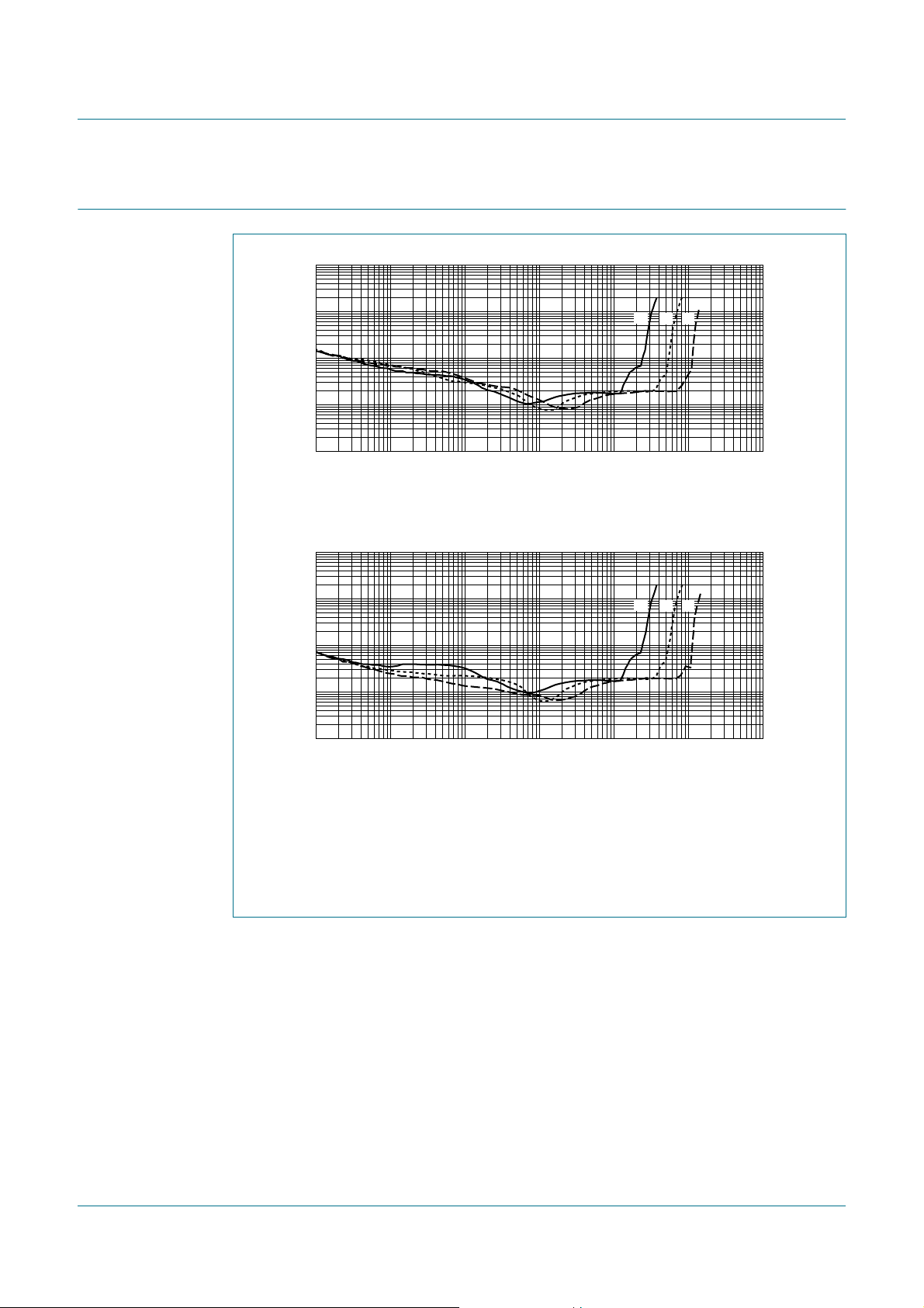
10. Typical performance curves
SA58670A
2.1 W/channel stereo class-D audio amplifier
10
THD+N
(%)
10
10
a. G
10
THD+N
(%)
10
10
−1
−2
10
−1
2
1
10
v(cl)
2
1
−5
=24dB
001aah484
(1)
(2) (3)
−4
10
−3
10
−2
10
−1
(1)
(2) (3)
Po (W)
10110
001aah485
−2
10
b. G
10
−5
v(cl)
= 6 dB.
−4
10
−3
10
−2
10
−1
Po (W)
10110
fi= 1 kHz.
(1) VDD= 2.5 V.
(2) VDD= 3.6 V.
(3) VDD= 5.0 V.
Fig 3. Total harmonic distortion-plus-noise as a function of output power; RL=8Ω
SA58670A_2 © NXP B.V. 2008. All rights reserved.
Product data sheet Rev. 02 — 23 October 2008 7 of 24
Page 8
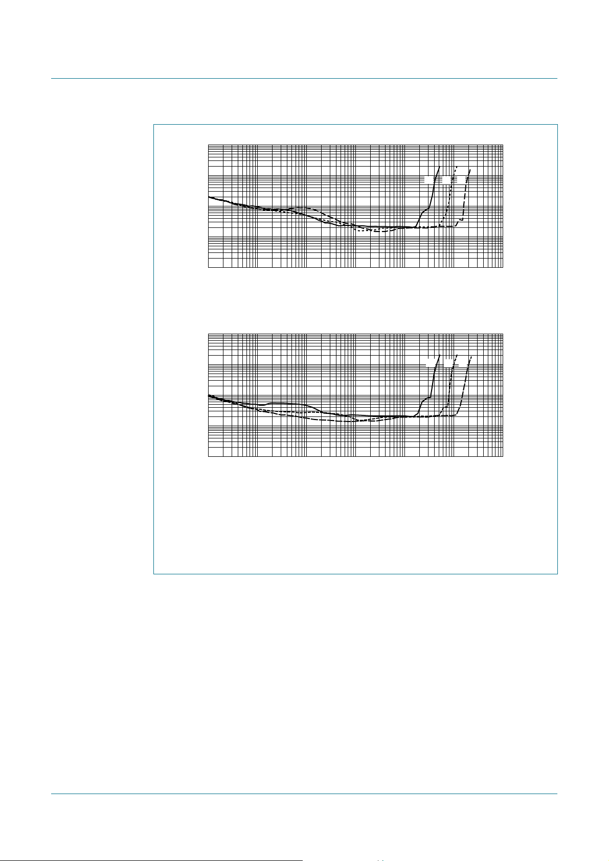
NXP Semiconductors
SA58670A
2.1 W/channel stereo class-D audio amplifier
10
THD+N
(%)
10
10
a. G
10
THD+N
(%)
10
2
10
1
−1
−2
10
2
10
1
−1
−5
v(cl)
=24dB.
001aah486
(1)
(2) (3)
−4
10
−3
10
−2
10
−1
(1)
Po (W)
(2) (3)
10110
001aah487
−2
10
b. G
10
−5
v(cl)
= 6 dB.
−4
10
−3
10
−2
10
−1
Po (W)
10110
fi= 1 kHz.
(1) VDD= 2.5 V.
(2) VDD= 3.6 V.
(3) VDD= 5.0 V.
Fig 4. Total harmonic distortion-plus-noise as a function of output power; RL=4Ω
SA58670A_2 © NXP B.V. 2008. All rights reserved.
Product data sheet Rev. 02 — 23 October 2008 8 of 24
Page 9

NXP Semiconductors
SA58670A
2.1 W/channel stereo class-D audio amplifier
1
THD+N
(%)
−1
10
−2
10
−3
10
10 10
(1)
(2)
(3)
2
10
3
10
4
10
(1) Po = 350 mW; Vi = 590 mV (RMS).
(2) Po = 240 mW; Vi = 490 mV (RMS).
(3) Po = 120 mW; Vi = 346 mV (RMS).
a. RL=4Ω
1
THD+N
(%)
10
−1
(1)
(2)
001aah488
5
f (Hz)
001aah489
(3)
−2
10
−3
10
10 10
2
10
3
10
4
10
f (Hz)
5
(1) Po = 260 mW; Vi = 721.1 mV (RMS).
(2) Po = 180 mW; Vi = 600 mV (RMS).
(3) Po = 90 mW; Vi = 424.3 mV (RMS).
b. RL=8Ω
G
=6dB.
v(cl)
Fig 5. Total harmonic distortion-plus-noise as a function of frequency; VDD= 2.5 V
SA58670A_2 © NXP B.V. 2008. All rights reserved.
Product data sheet Rev. 02 — 23 October 2008 9 of 24
Page 10

NXP Semiconductors
SA58670A
2.1 W/channel stereo class-D audio amplifier
1
THD+N
(%)
−1
10
−2
10
−3
10
10 10
(1)
(3)
(2)
2
10
3
10
4
10
(1) Po = 825 mW; Vi = 908.3 mV (RMS).
(2) Po = 550 mW; Vi = 741.6 mV (RMS).
(3) Po = 275 mW; Vi = 524.4 mV (RMS).
a. RL=4Ω
1
THD+N
(%)
10
−1
(1)
(2)
001aah490
5
f (Hz)
001aah491
−2
10
−3
10
10 10
(3)
2
10
3
10
4
10
f (Hz)
5
(1) Po = 560 mW; Vi = 1.058 V (RMS).
(2) Po = 375 mW; Vi = 866 mV (RMS).
(3) Po = 190 mW; Vi = 616.4 mV (RMS).
b. RL=8Ω
G
=6dB.
v(cl)
Fig 6. Total harmonic distortion-plus-noise as a function of frequency; VDD= 3.6 V
SA58670A_2 © NXP B.V. 2008. All rights reserved.
Product data sheet Rev. 02 — 23 October 2008 10 of 24
Page 11

NXP Semiconductors
SA58670A
2.1 W/channel stereo class-D audio amplifier
1
THD+N
(%)
−1
10
(1)
−2
10
−3
10
(2)
(3)
2
10 10
10
3
10
4
10
(1) Po = 1.65 W; Vi = 1.285 V (RMS).
(2) Po = 1.1 W; Vi = 1.05 V (RMS).
(3) Po = 550 mW; Vi = 741.6 mV (RMS).
a. RL=4Ω
10
THD+N
(%)
10
10
1
−1
−2
(1)
(2)
(3)
001aah492
5
f (Hz)
001aah493
−3
10
10 10
2
10
3
10
4
10
f (Hz)
5
(1) Po = 1.16 W; Vi = 1.523 V (RMS).
(2) Po = 775 mW; Vi = 1.245 V (RMS).
(3) Po = 380 mW; Vi = 871.8 mV (RMS).
b. RL=8Ω
G
=6dB.
v(cl)
Fig 7. Total harmonic distortion-plus-noise as a function of frequency; VDD= 5.0 V
SA58670A_2 © NXP B.V. 2008. All rights reserved.
Product data sheet Rev. 02 — 23 October 2008 11 of 24
Page 12

NXP Semiconductors
SA58670A
2.1 W/channel stereo class-D audio amplifier
−60
α
ct
(dB)
−80
(1)
(2)
−100
−120
10
(3)
(4)
3
4
10
f (Hz)
(1) VDD = 3.6 V; L channel to R channel.
(2) VDD = 3.6 V; R channel to L channel.
(3) VDD = 5.0 V; L channel to R channel.
(4) VDD = 5.0 V; R channel to L channel.
Fig 8. Crosstalk (stepped all-to-one) as a function of frequency
−3
10
001aah495
001aah497
5
10
V
n(o)
(V)
−4
10
(1)
(2)
−5
10
−6
10
10 10
2
10
3
(1) Left channel.
(2) Right channel.
Fig 9. Noise output voltage (RMS value) as a function of frequency
f (Hz)
4
10
SA58670A_2 © NXP B.V. 2008. All rights reserved.
Product data sheet Rev. 02 — 23 October 2008 12 of 24
Page 13

NXP Semiconductors
SA58670A
2.1 W/channel stereo class-D audio amplifier
−60
α
ct
(dB)
−80
−100
−120
2 20
(1)
(2)
(3)
8
144 6 10 12 16 18
a. RL=4Ω
−60
α
ct
(dB)
−80
001aah505
f (kHz)
001aah506
(1)
(2)
−100
−120
2 20
(3)
8
144 6 10 12 16 18
b. RL=8Ω
(1) VDD = 2.5 V.
(2) VDD = 3.6 V.
(3) VDD = 5.0 V.
Fig 10. Crosstalk (one-to-one) as a function of frequency
f (kHz)
SA58670A_2 © NXP B.V. 2008. All rights reserved.
Product data sheet Rev. 02 — 23 October 2008 13 of 24
Page 14

NXP Semiconductors
SA58670A
2.1 W/channel stereo class-D audio amplifier
V
SDR; VSDL
001aah507
5 V
(V)
6
V
DD
(V)
4
2
0
0321
3.6 V
2.5 V
Fig 11. Supply voltage as a function of shutdown
voltage
1600
I
DD
(mA)
1200
001aah509
5.5
I
DD
(mA)
4.5
3.5
2.5
2.5 5.54.53.5
001aah508
(1)
(2)
(3)
VDD (V)
(1) left channel; RL=8Ω.
(2) right channel; RL=4Ω.
(3) right channel; RL=8Ω.
Fig 12. Supply current as a function of supply voltage
001aah510
I
DD
(mA)
800
600
800
(1)
400
0
0 2.01.60.8 1.20.4
(2) (3)
P
(W)
o
a. RL=4Ω b. RL=8Ω
(1) VDD = 2.5 V.
(2) VDD = 3.6 V.
(3) VDD = 5.0 V.
Fig 13. Supply current as a function of output power
400
200
0
0 1.61.20.4 0.8
(1)
(2) (3)
P
(W)
o
SA58670A_2 © NXP B.V. 2008. All rights reserved.
Product data sheet Rev. 02 — 23 October 2008 14 of 24
Page 15

NXP Semiconductors
SA58670A
2.1 W/channel stereo class-D audio amplifier
0.8
P
(W)
0.6
0.4
0.2
0
0 2.01.60.8 1.20.4
(2)
(3)
001aah511
(1)
(W)
P
o
(W)
a. RL=4Ω b. RL=8Ω
(1) VDD = 5.0 V.
(2) VDD = 3.6 V.
(3) VDD = 2.5 V.
Fig 14. Power dissipation as a function of output power
100
η
po
80
60
(3)
(2)
001aah513
(1)
η
po
0.4
P
0.3
0.2
0.1
0
100
80
60
(3)
0 1.61.20.4 0.8
(3)
(2)
001aah512
(1)
(2)
(W)
P
o
001aah514
(1)
40
20
0
0 2.01.60.8 1.20.4
P
(W)
o
a. RL=4Ω b. RL=8Ω
(1) VDD = 5.0 V.
(2) VDD = 3.6 V.
(3) VDD = 2.5 V.
Fig 15. Output power efficiency as a function of output power
40
20
0
0 1.61.20.4 0.8
P
(W)
o
SA58670A_2 © NXP B.V. 2008. All rights reserved.
Product data sheet Rev. 02 — 23 October 2008 15 of 24
Page 16

NXP Semiconductors
11. Application information
SA58670A
2.1 W/channel stereo class-D audio amplifier
differential inputs
left channel
FB
FB
1 µF
INLP
G1
OUTLP
OUTLN
PVDD
1 µF
PGND
V
DD
1 nF
1 nF
V
DD
10 µF
1 µF
INLN
AGND
SA58670A
SDL SDR AVDD
differential inputs
right channel
1 µF
INRN
Fig 16. SA58670A application schematic
11.1 Power supply decoupling considerations
INRP
OUTRP
OUTRN
PVDD
PGND
1 µF
1 µF
G0
FB
FB
10 µF
V
DD
1 nF
1 nF
V
DD
10 µF1 µF
V
DD
002aad665
The SA58670A is a stereo class-D audio amplifier that requires proper supply voltage
decoupling to ensure the rated performance for THD+N and power efficiency. Todecouple
high frequency transients, supply voltage spikes and digital noise on the supply voltage
bus line, a low Equivalent Series Resistance (ESR) capacitor of typically 1 µF is placed as
close as possible to the PVDD pins of the SA58670A. It is important to place the
decoupling capacitor at the supply voltage pins of the SA58670A because any resistance
or inductance in the PCB trace between the SA58670A and the capacitor can cause a
loss in efficiency. Additional decoupling using a larger capacitor, 4.7 µF or greater,may be
done on the supply voltage connection on the PCB to filter low frequency signals. Usually
this is not required due to high PSRR of the SA58670A.
11.2 Input capacitor selection
The SA58670A does not require input coupling capacitors when used with a differential
audio source that is biased from 0.5 V to VDD− 0.8 V.In other words, the input signal must
be biased within the common-mode input voltage (V
required or if it is driven using a single-ended source, input coupling capacitors are
required.
The 3 dB cut-off frequency created by the input coupling capacitor and the input resistors
(see Table 6) is calculated by Equation 1:
f
=
3dB–
1
----------------------------- -
2π Ri× Ci×
) range. If high-pass filtering is
i(cm)
(1)
SA58670A_2 © NXP B.V. 2008. All rights reserved.
Product data sheet Rev. 02 — 23 October 2008 16 of 24
Page 17

NXP Semiconductors
Table 6. Gain selection
G1 G0 Gain (V/V) Gain (dB) Input impedance (kΩ)
LOW LOW 2 6 28.1
LOW HIGH 4 12 17.3
HIGH LOW 8 18 9.8
HIGH HIGH 16 24 5.2
Since the value of the input decoupling capacitor and the input resistance determined by
the gain setting affects the low frequency performance of the audio amplifier, it is
important to consider this during the system design. Small speakers in wireless and
cellular phones usually do not respond well to low frequency signals, so the 3 dB cut-off
frequency may be increased to block the low frequency signals to the speakers. Not using
input coupling capacitors may increase the output offset voltage.
Equation 2 is solved for Ci:
SA58670A
2.1 W/channel stereo class-D audio amplifier
C
=
i
1
--------------------------------------
2π Ri× f
×
3dB–
11.3 PCB layout considerations
Component location is very important for performance of the SA58670A. Place all
external components very close to the SA58670A. Placing decoupling capacitors directly
at the power supply voltage pins increases efficiency because the resistance and
inductance in the trace between the SA58670A power supply voltage pins and the
decoupling capacitor causes a loss in power efficiency.
The trace width and routing are also very important for power output and noise
considerations.
For high current pins (PVDD, PGND and audio output), the trace widths should be
maximized to ensure proper performance and output power. Use at least 500 µm wide
traces.
For the input pins (INRP, INRN, INLP and INLN), the traces must be symmetrical and run
side-by-side to maximize common-mode cancellation.
11.4 Filter-free operation and ferrite bead filters
A ferrite bead low-pass filter can be used to reduce radio frequency emissions in
applications that have circuits sensitive to frequencies greater than 1 MHz. A ferrite bead
low-pass filter functions well for amplifiers that must pass FCC unintentional radiation
requirements for frequencies greater than 30 MHz. Choose a bead with high-impedance
at high frequencies and very low-impedance at low frequencies. In order to prevent
distortion of the output signal, select a ferrite bead with adequate current rating.
(2)
For applications in which there are circuits that are EMI sensitive to low frequencies
(< 1 MHz) and there are long leads from amplifier to speaker,it is necessary to use an LC
output filter.
SA58670A_2 © NXP B.V. 2008. All rights reserved.
Product data sheet Rev. 02 — 23 October 2008 17 of 24
Page 18

NXP Semiconductors
11.5 Efficiency and thermal considerations
The maximum ambient operating temperature depends on the heat transferring ability of
the heat spreader on the PCB layout. In Table 3 “Limiting values”, the power derating
factoris given as 41.6 mW/K. The device thermal resistance, R
power derating factor. Convert the power derating factor to R
SA58670A
2.1 W/channel stereo class-D audio amplifier
is the reciprocal of the
th(j-a)
by Equation 3:
th(j-a)
R
th j-a()
----------------------------------------- -
derating factor
1
1
----------------
0.0416
For a maximum allowable junction temperature Tj= 150 °C and R
maximum device dissipation of 1.5 W (750 mW per channel) and for 2.1 W per channel
output power, 4 Ω load, 5 V supply, the maximum ambient temperature is calculated using
Equation 4:
T
amb max()Tj max()Rth j-a()Pmax
×()– 150 24 1.5×()– 114 °C===
The maximum ambient temperature is 114 °C at maximum power dissipation for 5 V
supply and 4 Ω load. If the junction temperature of the SA58670A rises above 150 °C, the
thermal protection circuitry turns the SA58670A off; this prevents damage to IC. Using
speakers greater than 4 Ω further enhances thermal performance and battery lifetime by
reducing the output load current and increasing amplifier efficiency.
11.6 Additional thermal information
The SA58670A HVQFN20 package incorporates an exposed DAP that is designed to
solder the mount directly to the PCB heat spreader. By the use of thermal vias, the DAP
may be soldered directly to a ground plane or special heat sinking layer designed into the
PCB. The thickness and area of the heat spreader may be maximized to optimize heat
transfer and achieve lowest package thermal resistance.
24 K/W===
= 24 K/W and a
th(j-a)
(3)
(4)
12. Test information
15 µH
AP585
AUDIO
ANALYZER
INxP
INxN
Fig 17. Test circuit
SA58670A_2 © NXP B.V. 2008. All rights reserved.
Product data sheet Rev. 02 — 23 October 2008 18 of 24
DUT
+
POWER
SUPPLY
OUTxP
OUTxN
−
15 µH
R
L
LOW-PASS FILTER
MEASUREMENT
AUX0025
30 kHz
AP585
INPUTS
002aad417
Page 19

NXP Semiconductors
2.1 W/channel stereo class-D audio amplifier
13. Package outline
HVQFN20: plastic thermal enhanced very thin quad flat package; no leads;
20 terminals; body 4 x 4 x 0.85 mm
A
D
terminal 1
index area
B
SA58670A
SOT917-1
E
e
1
e
D
4.1
3.9
b
11
15
D
h
0 2.5 5 mm
D
2.45
2.15
h
(1)
E
E
4.1
2.45
3.9
2.15
REFERENCES
(1)
610
L
5
E
h
1
terminal 1
index area
DIMENSIONS (mm are the original dimensions)
(1)
A
UNIT
mm
Note
1. Plastic or metal protrusions of 0.075 mm maximum per side are not included.
OUTLINE
VERSION
SOT917 -1 MO-220- - - - - -
max.
A
0.05
0.00
1
0.30
0.18
20 16
c
b
0.2
IEC JEDEC JEITA
v
M
w
M
e
e
2
scale
h
0.51
A
A
1
detail X
C
0.6
0.4
L
y
C
1
w
0.1v0.05
ye
y
0.05 0.1
EUROPEAN
PROJECTION
X
ACCB
e
e
1
2
2
2
c
y
1
ISSUE DATE
05-10-08
05-10-31
Fig 18. Package outline SOT917-1 (HVQFN20)
SA58670A_2 © NXP B.V. 2008. All rights reserved.
Product data sheet Rev. 02 — 23 October 2008 19 of 24
Page 20

NXP Semiconductors
14. Soldering of SMD packages
This text provides a very brief insight into a complex technology. A more in-depth account
of soldering ICs can be found in Application Note
soldering description”
14.1 Introduction to soldering
Soldering is one of the most common methods through which packages are attached to
Printed Circuit Boards (PCBs), to form electrical circuits. The soldered joint provides both
the mechanical and the electrical connection. There is no single soldering method that is
ideal for all IC packages. Wave soldering is often preferred when through-hole and
Surface Mount Devices (SMDs) are mixed on one printed wiring board; however, it is not
suitable for fine pitch SMDs. Reflow soldering is ideal for the small pitches and high
densities that come with increased miniaturization.
14.2 Wave and reflow soldering
Wave soldering is a joining technology in which the joints are made by solder coming from
a standing wave of liquid solder. The wave soldering process is suitable for the following:
.
SA58670A
2.1 W/channel stereo class-D audio amplifier
AN10365 “Surface mount reflow
• Through-hole components
• Leaded or leadless SMDs, which are glued to the surface of the printed circuit board
Not all SMDs can be wave soldered. Packages with solder balls, and some leadless
packages which have solder lands underneath the body, cannot be wave soldered. Also,
leaded SMDs with leads having a pitch smaller than ~0.6 mm cannot be wave soldered,
due to an increased probability of bridging.
The reflow soldering process involves applying solder paste to a board, followed by
component placement and exposure to a temperature profile. Leaded packages,
packages with solder balls, and leadless packages are all reflow solderable.
Key characteristics in both wave and reflow soldering are:
• Board specifications, including the board finish, solder masks and vias
• Package footprints, including solder thieves and orientation
• The moisture sensitivity level of the packages
• Package placement
• Inspection and repair
• Lead-free soldering versus SnPb soldering
14.3 Wave soldering
Key characteristics in wave soldering are:
• Process issues, such as application of adhesive and flux, clinching of leads, board
transport, the solder wave parameters, and the time during which components are
exposed to the wave
• Solder bath specifications, including temperature and impurities
SA58670A_2 © NXP B.V. 2008. All rights reserved.
Product data sheet Rev. 02 — 23 October 2008 20 of 24
Page 21

NXP Semiconductors
14.4 Reflow soldering
Key characteristics in reflow soldering are:
• Lead-freeversus SnPb soldering; note that a lead-free reflow process usually leads to
• Solder paste printing issues including smearing, release, and adjusting the process
• Reflow temperature profile; this profile includes preheat, reflow (in which the board is
Table 7. SnPb eutectic process (from J-STD-020C)
Package thickness (mm) Package reflow temperature (°C)
< 2.5 235 220
≥ 2.5 220 220
SA58670A
2.1 W/channel stereo class-D audio amplifier
higher minimum peak temperatures (see Figure 19) than a SnPb process, thus
reducing the process window
window for a mix of large and small components on one board
heated to the peak temperature) and cooling down. It is imperative that the peak
temperature is high enough for the solder to make reliable solder joints (a solder paste
characteristic). In addition, the peak temperature must be low enough that the
packages and/or boards are not damaged. The peak temperature of the package
depends on package thickness and volume and is classified in accordance with
Table 7 and 8
Volume (mm3)
< 350 ≥ 350
Table 8. Lead-free process (from J-STD-020C)
Package thickness (mm) Package reflow temperature (°C)
Volume (mm3)
< 350 350 to 2000 > 2000
< 1.6 260 260 260
1.6 to 2.5 260 250 245
> 2.5 250 245 245
Moisture sensitivity precautions, as indicated on the packing, must be respected at all
times.
Studies have shown that small packages reach higher temperatures during reflow
soldering, see Figure 19.
SA58670A_2 © NXP B.V. 2008. All rights reserved.
Product data sheet Rev. 02 — 23 October 2008 21 of 24
Page 22

NXP Semiconductors
Fig 19. Temperature profiles for large and small components
maximum peak temperature
temperature
MSL: Moisture Sensitivity Level
= MSL limit, damage level
minimum peak temperature
= minimum soldering temperature
SA58670A
2.1 W/channel stereo class-D audio amplifier
peak
temperature
time
001aac844
For further information on temperature profiles, refer to Application Note
“Surface mount reflow soldering description”
15. Abbreviations
Table 9. Abbreviations
Acronym Description
DAP Die Attach Paddle
DVD Digital Video Disc
EMI ElectroMagnetic Interference
ESR Equivalent Series Resistance
LC inductor-capacitor filter
PC Personal Computer
PCB Printed-Circuit Board
PDA Personal Digital Assistant
PWM Pulse Width Modulator
USB Universal Serial Bus
16. Revision history
AN10365
.
Table 10. Revision history
Document ID Release date Data sheet status Change notice Supersedes
SA58670A_2 20081023 Product data sheet - SA58670A_1
Modifications:
SA58670A_1 20080220 Product data sheet - -
SA58670A_2 © NXP B.V. 2008. All rights reserved.
Product data sheet Rev. 02 — 23 October 2008 22 of 24
• Table 4 “Static characteristics”:
– added I
specification
DD(sd)
Page 23

NXP Semiconductors
17. Legal information
17.1 Data sheet status
SA58670A
2.1 W/channel stereo class-D audio amplifier
Document status
Objective [short] data sheet Development This document contains data from the objective specification for product development.
Preliminary [short] data sheet Qualification This document contains data from the preliminary specification.
Product [short] data sheet Production This document contains the product specification.
[1] Please consult the most recently issued document before initiating or completing a design.
[2] The term ‘short data sheet’ is explained in section “Definitions”.
[3] The product status of device(s) described in this document may have changed since this document was published and may differ in case of multiple devices. The latest product status
information is available on the Internet at URL
[1][2]
Product status
17.2 Definitions
Draft — The document is a draft version only. The content is still under
internal review and subject to formal approval, which may result in
modifications or additions. NXP Semiconductors does not give any
representations or warranties as to the accuracy or completeness of
information included herein and shall haveno liability for the consequences of
use of such information.
Short data sheet — A short data sheet is an extract from a full data sheet
with the same product type number(s) and title. A short data sheet is intended
for quick reference only and should not be relied upon to contain detailed and
full information. For detailed and full information see the relevant full data
sheet, which is available on request via the local NXP Semiconductors sales
office. In case of any inconsistency or conflict with the short data sheet, the
full data sheet shall prevail.
17.3 Disclaimers
General — Information in this document is believed to be accurate and
reliable. However, NXP Semiconductors does not give any representations or
warranties, expressedor implied, as to the accuracy or completeness of such
information and shall have no liability for the consequences of use of such
information.
Right to make changes — NXP Semiconductors reserves the right to make
changes to information published in this document, including without
limitation specifications and product descriptions, at any time and without
notice. This document supersedes and replaces all information supplied prior
to the publication hereof.
Suitability for use — NXP Semiconductors products are not designed,
authorized or warranted to be suitable for use in medical, military, aircraft,
space or life support equipment, nor in applications where failure or
[3]
http://www.nxp.com.
Definition
malfunction of an NXP Semiconductors product can reasonably be expected
to result in personal injury, death or severe property or environmental
damage. NXP Semiconductors accepts no liability for inclusion and/or use of
NXP Semiconductors products in such equipment or applications and
therefore such inclusion and/or use is at the customer’s own risk.
Applications — Applications that are described herein for any of these
products are for illustrative purposes only. NXP Semiconductors makes no
representation or warranty that such applications will be suitable for the
specified use without further testing or modification.
Limiting values — Stress above one or more limiting values (as defined in
the Absolute Maximum Ratings System of IEC 60134) may cause permanent
damage to the device. Limiting values are stress ratings only and operation of
the device at these or any other conditions above those given in the
Characteristics sections of this document is not implied. Exposure to limiting
values for extended periods may affect device reliability.
Terms and conditions of sale — NXP Semiconductors products are sold
subject to the general terms and conditions of commercial sale, as published
at
http://www.nxp.com/profile/terms, including those pertaining to warranty,
intellectual property rights infringement and limitation of liability, unless
explicitly otherwise agreed to in writing by NXP Semiconductors. In case of
any inconsistency or conflict between information in this document and such
terms and conditions, the latter will prevail.
No offer to sell or license — Nothing in this document may be interpreted
or construed as an offer to sell products that is open for acceptance or the
grant, conveyanceor implication of any license under any copyrights, patents
or other industrial or intellectual property rights.
17.4 Trademarks
Notice: All referencedbrands, product names, service names and trademarks
are the property of their respective owners.
18. Contact information
For more information, please visit: http://www.nxp.com
For sales office addresses, please send an email to: salesaddresses@nxp.com
SA58670A_2 © NXP B.V. 2008. All rights reserved.
Product data sheet Rev. 02 — 23 October 2008 23 of 24
Page 24

NXP Semiconductors
19. Contents
1 General description. . . . . . . . . . . . . . . . . . . . . . 1
2 Features . . . . . . . . . . . . . . . . . . . . . . . . . . . . . . . 1
3 Applications . . . . . . . . . . . . . . . . . . . . . . . . . . . . 1
4 Ordering information. . . . . . . . . . . . . . . . . . . . . 2
5 Block diagram . . . . . . . . . . . . . . . . . . . . . . . . . . 2
6 Pinning information. . . . . . . . . . . . . . . . . . . . . . 3
6.1 Pinning . . . . . . . . . . . . . . . . . . . . . . . . . . . . . . . 3
6.2 Pin description . . . . . . . . . . . . . . . . . . . . . . . . . 3
7 Limiting values. . . . . . . . . . . . . . . . . . . . . . . . . . 4
8 Static characteristics. . . . . . . . . . . . . . . . . . . . . 5
9 Dynamic characteristics . . . . . . . . . . . . . . . . . . 6
10 Typical performance curves . . . . . . . . . . . . . . . 7
11 Application information. . . . . . . . . . . . . . . . . . 16
11.1 Power supply decoupling considerations . . . . 16
11.2 Input capacitor selection. . . . . . . . . . . . . . . . . 16
11.3 PCB layout considerations . . . . . . . . . . . . . . . 17
11.4 Filter-free operation and ferrite bead filters. . . 17
11.5 Efficiency and thermal considerations . . . . . . 18
11.6 Additional thermal information . . . . . . . . . . . . 18
12 Test information. . . . . . . . . . . . . . . . . . . . . . . . 18
13 Package outline . . . . . . . . . . . . . . . . . . . . . . . . 19
14 Soldering of SMD packages . . . . . . . . . . . . . . 20
14.1 Introduction to soldering . . . . . . . . . . . . . . . . . 20
14.2 Wave and reflow soldering . . . . . . . . . . . . . . . 20
14.3 Wave soldering. . . . . . . . . . . . . . . . . . . . . . . . 20
14.4 Reflow soldering. . . . . . . . . . . . . . . . . . . . . . . 21
15 Abbreviations. . . . . . . . . . . . . . . . . . . . . . . . . . 22
16 Revision history. . . . . . . . . . . . . . . . . . . . . . . . 22
17 Legal information. . . . . . . . . . . . . . . . . . . . . . . 23
17.1 Data sheet status . . . . . . . . . . . . . . . . . . . . . . 23
17.2 Definitions. . . . . . . . . . . . . . . . . . . . . . . . . . . . 23
17.3 Disclaimers. . . . . . . . . . . . . . . . . . . . . . . . . . . 23
17.4 Trademarks. . . . . . . . . . . . . . . . . . . . . . . . . . . 23
18 Contact information. . . . . . . . . . . . . . . . . . . . . 23
19 Contents. . . . . . . . . . . . . . . . . . . . . . . . . . . . . . 24
SA58670A
2.1 W/channel stereo class-D audio amplifier
Please be aware that important notices concerning this document and the product(s)
described herein, have been included in section ‘Legal information’.
© NXP B.V. 2008. All rights reserved.
For more information, please visit: http://www.nxp.com
For sales office addresses, please send an email to: salesaddresses@nxp.com
Date of release: 23 October 2008
Document identifier: SA58670A_2
 Loading...