

Page 1

NXP Semiconductors
Application Note
Document Number: AN5251
Rev. 1, 04/2018
S32R27/37 Hardware Design Guide
by: NXP Semiconductors
Contents
1 Introduction
The S32R is a 32-bit heterogeneous multi-core microcontroller
family primarily intended for use in computationally intensive
automotive RADAR applications. The device family
incorporates Power Architecture® cores arranged as two
independent e200z7260 for general computation and the
S32R274 device also features an e200z420 core with an
e200z419 checker core running in delayed lockstep
configuration for safety-critical and housekeeping tasks. The
family integrates high-performance signal processing features
designed to support sophisticated automotive RADAR
applications, and the S32R274 also integrates high accuracy
analog features to further enhance it's ability to interface with
a wide range of RADAR RF devices.
This application note illustrates the S32R family power supply
options and details the external circuitry required for power
supplies, oscillator connections, and supply decoupling pins. It
also discusses configuration options for clock, reset, ADC
modules and the RADAR analog front-end, as well as
recommended debug and peripheral communication
connections (including MIPI-CSI2) and other major external
hardware required for the device.
The S32R family requires multiple external power supplies to
operate. The main cores internal logic requires a 1.25 V power
supply. This can be supplied from an external source or on
some devices this can alternatively be provided by an internal
DC-DC regulator that requires a dedicated supply. 3.3 V is
1 Introduction.............................. .............................. 1
2 S32R family package options
overview.................................................................. 2
3 Power supply...........................................................3
4 Clock configuration...............................................15
5 Device reset configuration............... .....................17
6 Recommended debug connectors and
connector pin-out definitions.................... ............ 18
7 ADC overview........................... ........................... 22
8 RADAR analog front end..................................... 23
9 Example communication peripheral
connections.......................................... ................. 29
10 High speed layout considerations..........................48
A Revision History................................................... 49
Page 2
S32R family package options overview
required for the general purpose I/O, flash memory, analog front-end, external communications interfaces, and on-chip SAR
analog to digital converter.
2 S32R family package options overview
The S32R family is available in multiple device and package options that are suited to development, debug and commercial
production.
Table 1. S32R package description
Device Package Description
S32R274 257 Map ball grid array (MAPBGA) Full support for all device modules and features
including JTAG and Nexus High Speed Aurora Trace
debug interfaces.
S32R372 257 Map ball grid array (MAPBGA) Full support for all device modules and features
including JTAG and Nexus High Speed Aurora Trace
debug interfaces. Pin compatible with S32R274,
although with reduced feature set. See Table 3 below
for details.
S32R372 141 Map ball grid array (MAPBGA) Reduced support for some device modules and
features. See Table 3 for details of reduced features
The table below shows the physical dimensions of the packages. See the device data sheet for complete package dimensions
and ball placement. Drawings are also available on nxp.com, search for the case outline number shown in Table 2.
Table 2. Package sizes
Device Package Physical Size Case Outline Number Pitch
S32R274 257 MAPBGA 14 x 14 mm 98ASA00081D 0.8 mm
S32R372 257 MAPBGA 14 x 14 mm 98ASA00081D 0.8 mm
S32R372 141 MAPBGA 10 x 10 mm 84ASA00768D 0.65 mm
The table below shows the main differences between the S32R family, including the different available packages. This list
only references the differences that have a hardware impact. For full details of all differences between the various devices
please see the relevant device reference manuals.
Table 3. Feature Differences Between Packages
Feature S32R274 S32R372 257 MAPBGA S32R372 141 MAPBGA
SD-ADC 4x SD-ADC None None
DAC Yes None None
MIPI CSI2 4 Lanes + Clock 2 Lanes + Clock 2 Lanes + Clock
Ethernet Yes, up to RGMII interface. None None
Wave Generator Module
(WGM)
LINFlexD Yes, 1 module Yes, 1 module None
FlexPWM 1 module, 12 channels 1 module, 12 channels 1 module, 11 channels
Yes None None
Table continues on the next page...
S32R27/37 Hardware Design Guide, Rev. 1, 04/2018
2 NXP Semiconductors
Page 3

Power supply
Table 3. Feature Differences Between Packages (continued)
Feature S32R274 S32R372 257 MAPBGA S32R372 141 MAPBGA
SPI 2 modules 2 modules 2 modules, some chip selects not
available. See device muxing
sheet for details.
IIC 2 modules 2 modules 1 module (IIC1 only).
Serial Inter-Processor
Interface (SIPI)
System Timer Module
(STM)
System Timer Module
(STM)
FlexRay 1 module None None
FlexCAN 1x FlexCAN, 2x FlexCAN-FD2x FlexCAN-FD 2x FlexCAN-FD
Yes None None
3 modules x 4 channels 2 modules x 4 channels 2 modules x 4 channels
eTimer_0: 6 channels,
eTimer_1: 6 channels
eTimer_1:6 channels eTimer_1:5 channels
Device Power Supply Internal or External
regulation modes
Internal or External regulation
modes
External regulation mode only
3 Power supply
The S32R family of microcontroller units have a robust power management infrastructure that enables applications to select
among various user modes and to monitor internal voltages for high- and low-voltage conditions. The monitoring capability
is also used to ensure supply voltages and internal voltages are within the required operating ranges before the
microcontroller can exit the reset state and enter operation.
The microcontroller offers a DC-DC voltage regulator function as part of the power management controller (PMC) module.
This regulator can be used to supply the digital low voltage required for the internal logic and other low voltage supplies. The
device can be configured to use either this internal regulation mode or an external 1.25 V regulated power supply to provide
the core voltage. The standard configuration utilizes the internal DC-DC voltage regulator, with the following external supply
voltages:
• 3.3 V for main general purpose I/O, SAR ADC supply and reference, JTAG debug interface, flash memory supply
voltage and external communication interfaces (Ethernet, FlexRay, etc.)
• 3.13 - 5.5 V (required) for the internal DC-DC voltage regulator which supplies 1.25 V for the internal logic, PLL
circuits and low voltage/Nexus Aurora I/O, and MIPI-CSI2.
Detailed information on the power management configurations can be found in the Power management controller section.
1
1. Not available on the S32R372 141BGA Package.
S32R27/37 Hardware Design Guide, Rev. 1, 04/2018
NXP Semiconductors 3
Page 4
Power supply
3.1 Power supply signals and decoupling
Table 4 lists all MCU power domains with corresponding pin names. Depending on the power management configuration,
some of the supplies below may not require an external power source. The power management configuration is detailed in
Power management controller.
Table 4. MCU power supply pins
Domain name Supply
Voltage
VDD_LV_CORE 1.25 V Low-voltage supply for core logic
VDD_HV_IOx 3.3 V High-voltage supply for general purpose I/O
VDD_HV_RAW 3.3 V High-voltage, high fidelity supply for analog front-end block
VDD_HV_DAC
VDD_HV_ADC 3.3 V Voltage supply for SAR ADC module
VDD_HV_ADCREF0/2
VDD_HV_FLA 3.3 V Voltage supply for flash memory
VDD_HV_PMU 3.3 V Voltage supply for power management unit
VDD_HV_IO_PWM
VDD_HV_REG3V8
VDD_LV_LFASTPLL
VDD_LV_IO_AURORA
VDD_LV_PLL0 1.25 V Voltage supply for system PLL
VDD_LV_IO 1.25 V Low voltage supply for general purpose I/O
VDD_LV_DPHY
1. Not present on S32R372 141MAPBGA Package
2. To ensure optimum SAR ADC performance it is recommended to have a ground plane below the VDD_HV_ADCREF0/2
traces.
3. Internal regulation mode. When using external regulation mode, this domain can be tied to VDD_HV_PMU
4. The naming convention VDD_LV_LFASTPLL is equal to VDD_LV_DRFPLL. Not present on S32R372 141MAPBGA
Package
5. VDD_LV_IO_AURORA must be connected to the same voltage supply as VDD_LV_CORE. The supplies must be brought
up simultaneously.
6. Can be supplied from VDD_LV_CORE supply with filtering as recommended below.
1
2
1
1
4
5
6
3.3 V High-voltage supply for DAC module in analog front-end
3.3 V Voltage reference for SAR ADC 0/2
3.3 V Voltage supply for PWM IO
3.13 V - 5.5 V
1.25 V Voltage supply for DigiRF (SIPI/LFAST) PLL
1.25 V Voltage supply for Nexus Aurora I/O
1.25 V Low voltage supply for MIPI-CSI2 DHPY
3
Voltage supply for internal DC-DC voltage regulator
Description
Some of the supplies can be powered with different supply voltages. The internal voltage regulator supply,
VDD_HV_REG3V8, can be supplied with a voltage between 3.13 V and 5.5 V. See the device data sheet for specific
information and to learn what voltage ranges can be safely connected to the power pins.
Table 5 shows all power domains and the suggested decoupling and/or filter capacitors for their corresponding pins. These
values are provided as a guideline and will vary depending on the application and capability of the power supplies used.
The decoupling capacitors must be placed as close as possible to the MCU supply pins, with priority given to those with the
smallest capacitance value.
Table 5. Supply pin decoupling capacitors
Domain name Supply
Voltage
VDD _LV_CORE 1.25 V 0.1 μF x 16, 4.7 μF x 4, 10 μF x 2 (40 μF total)
VDD_HV_IOx 3.3 V 2 x 0.1 μF for each VDD_HV_IO supply
Table continues on the next page...
S32R27/37 Hardware Design Guide, Rev. 1, 04/2018
4 NXP Semiconductors
Minimum Decoupling Capacitors
1
2
Page 5
Table 5. Supply pin decoupling capacitors (continued)
Power supply
Domain name Supply
Voltage
VDD_HV_RAW 3.3 V 0.1 μF, 1 μF
VDD_HV_DAC
VDD_HV_ADC 3.3 V 0.1 μF, 1 μF
VDD_HV_ADCREF0/2 3.3 V 0.01 μF, 1 μF
VDD_HV_IO_PWM
VDD_HV_FLA 3.3 V 0.1 μF, 1000 pF
VDD_HV_PMU 3.3 V 100 nF, 4.7 μF
VDD_HV_REG3V8
VDD_LV_DRFPLL
VDD_LV_IO_AURORA 1.25 V 0.1 μF, 1 μF
VDD_LV_PLL0 1.25 V 1000 pF, 0.1 μF, 1μF, 0.01 μF
VDD_LV_DPHY 1.25 V Ferrite bead, >5 μF, 100 nF, 1000 pF
1. When using internal regulation mode, assure that the total capacitance (accounting for temperature variations) never falls
below 40 μF
2. External capacitors for the IO pins are dependent on the application.
3. Not present on S32R372 141BGA Package
4. When device is configured in external regulation mode and supply is connected to VDD_HV_PMU. For internal regulation
mode see SMPS external component configuration
3
3
3
3
3.3 V 1000 pF, 0.1 μF, 1 μF
3.3 V 2x 0.1 μF for each supply
3.13 V - 5.5
V
1.25 V 1000 pF, 0.1 μF, 1 μF, 0.01 μF
Minimum Decoupling Capacitors
1 μF Ceramic
4
The device has several pins for the connection to external decoupling capacitors for the analog front-end. Details of these can
be found in RADAR analog front end
3.2
Decoupling capacitors layout priority
When trade-offs must be made in the schematic layout, it is important to ensure that the highest priority supplies have
decoupling capacitors placed as closely as possible to the MCU. The list below outlines the recommended order of the
supplies from highest to lowest priority in terms of their importance for decoupling.
1. VDD_HV_RAW & VDD_HV_DAC
2. VDD_HV_ADCREF0/2
3. VDD_HV_ADC
4. VDD_LV_PLL0
5. VDD_LV_DPHY
6. VDD_LV_CORE
7. VDD_LV_AURORA
8. VDD_HV_PMU
9. VDD_HV_FLA
10. VDD_LV_LFASTPLL
2
11. VDD_LV_IO
12. VDD_HV_PWM
3
13. VDD_HV_IO
2. Not present on S32R372 141MAPBGA Package
3. Not present on S32R372 141MAPBGA Package
S32R27/37 Hardware Design Guide, Rev. 1, 04/2018
NXP Semiconductors 5
Page 6
Power supply
Highest priority is given to the high-fidelity analog front end supplies VDD_HV_RAW and VDD_HV_DAC, as their
decoupling must be prioritized to maintain analog signal integrity. VDD_HV_ADRREF0, VDD_HV_ADREF1, and
VDD_HV_ADC is the SAR analog-to-digital converters reference and power supply decoupling. Clean supplies are vital to
ensure that the highest accuracy is achieved with the ADCs. The supply for the system PLL is prioritized as this helps to
ensure reliable and stable operation from the internal PLL circuit.
Medium priority is given to VDD_LV_CORE, VDD_LV_DRFPLL, VDD_LV_AURORA, VDD_HV_PMU,
VDD_LV_DPHY and VDD_HV_FLA. VDD_LV_CORE is the main supply for the on-chip digital logic and this is
prioritized as it affects the largest amount of logic on the device. VDD_LV_AURORA powers the high speed Nexus Aurora
pins and noise on this domain would affect the quality of the output. VDD_HV_PMU is the power management unit supply
and VDD_LV_DPHY is the MIPI-CSI2 DPHY supply. The MIPI-CSI2 DPHY is a high speed module which requires
minimal noise in order to acheive the specified performance levels. VDD_HV_FLA is the input supply for the flash memory.
A good supply to the flash memory ensures reliable flash programming and erasing.
VDD_LV_LFASTPLL powers the PLL for the LFAST/SIPI communication interface. 4 VDD_HV_IO, VDD_HV_PWM,
and VDD_LV_IO drive GPIO and other external communication interfaces. Although it is still important that these supplies
have a clean power signal, the hardware they power is less affected by noise and they are considered of lower priority.
When completing the layout of decoupling capacitors care should be taken to reduce the volume of the space in the
transmission line between the device and the capacitor, which results in faster response to energy requests from the device.
The capacitor should always be the closest to the device so that the energy comes from the capacitor and not from the power
trace, as illustrated in the figure below.
Figure 1. Decoupling capacitor placement recommendation
3.3
The S32R family has a dedicated module for configuration and monitoring of power supplies, enable signals, internal
component trimming, and power-on reset generation. The Power Management Controller (PMC) consists of an analog block
and a supporting digital interface that provides control over the analog components. The PMC chapter in the device reference
manual explores the digital block in depth.
4. This interface is not present on the S32R372 device, but the supply name remains the same for the 257MAPBGA
6 NXP Semiconductors
Power management controller
package to avoid confusion, and is not present on the 141MAPBGA package.
S32R27/37 Hardware Design Guide, Rev. 1, 04/2018
Page 7
Power supply
NOTE
This document will focus on the external hardware and connections concerned with the
PMC analog block.
3.3.1 Core supply options
The S32R family offers two options for supplying the 1.25 V used by the core and other low-voltage digital power domains.
• Internal voltage regulation mode, using the integrated DC-DC voltage regulator (VREG)
• External voltage regulation mode using an externally regulated 1.25 V supply
5
The input pin VREG_SEL allows selection between internal and external regulation modes, the function of this input is
described in the table below.
6
Table 6. VREG_SEL input signal
Input Level Core Supply Mode
High (3.3 V) Internal regulation mode
Low (GND) External regulation mode
The PMC has an internal voltage regulator function that uses a switched-mode power supply (SMPS) circuit to supply the
1.25 V required by the internal core logic, VDD_LV_CORE and the other low-voltage digital supplies
(VDD_LV_AURORA, VDD_LV_PLL0, VDD_LV_DPHY and VDD_LV_IO). The regulator requires the support of
external circuitry detailed in SMPS external component configuration. This configuration is an asynchronous buck regulator
with nominal switching frequency of 1 MHz. The switching frequency may be modulated to improve the EMI performance
of the device, further information on this feature can be found in the PMC chapter in the device reference manual.
VREG_SEL is part of a collection of I/O signals that relate to the VREG operation mode. The other pins are mentioned in the
table below.
Table 7. PMC Voltage regulator signals
Signal Name Direction VREG Enabled (Internal Mode) VREG Disabled (External Mode)
VREG_POR_B Input External power-on reset. If not used it is
recommended to be externally pulled up
to 3.3 V, but can be left floating.
Internally pulled up to 3.3 V.
VREG_ISENS
VREG_SWP
1
1
Input Current sense input to internal regulator Not used. Connect to VDD_LV_CORE
Output Output from internal VREG. Controls the
gate of the external switching PMOS
transistor
2
Power-on reset (POR) input. Used by
external circuitry to trigger a POR or hold
device in reset state. Should be used to
hold device in reset until supplies are
within the ranges described in the device
data sheet.
Not used, can be left floating. Internally
pulled up, do not connect to GND.
1. Not present on S32R372 141MAPBGA package.
2. If the connection between VREG_SWP and the PMOS gate is broken, the switch may fully turn on. For added protection
against this risk, a 100 Kilo Ohm resistor can be connected between VDD_HV_REG3V8 and the PMOS gate.
5. Not supported on S32R372 141MAPBGA package.
6. VREG_SEL pad is internally bonded to GND on S32R372 141MAPBGA package.
S32R27/37 Hardware Design Guide, Rev. 1, 04/2018
NXP Semiconductors 7
Page 8
DC-DC
VReg
Board supply 5V -12V
DC-DC
VReg
SWP
SAR ADC
3.3V
low noise
POR
Lin.
VReg
3.3V
low noise
Lin.
VReg
Lin.
VReg
POR_B
DC-DC
VReg
AFE
Internal Lin. VRegs
3.3V
low noise
HV_PMU
3.3V
HV_REG_3V8
3.13V - 5.5V
LV_DRFPLL
LV_PLL0
LFAST
PLL
System
PLL
HV_ADCREF0/2
HV_ADC
1.25V
HV_DAC
HV_RAW
LV_IO_AURORA
NEXUS
AURORA
See "SMPS
External
Component
Configuration"
LV_DPHY
MIPI
CSI2
HV_FLA
HV_IOx
ISENS
LV_CORE
1.25V, 1.8A
HV_IO_PWM
Power supply
3.3.2 Internal voltage regulator supply mode
The standard device configuration for the S32R family 257 MAPBGA packages uses the internal DC-DC voltage regulator to
supply the core voltage and other low-voltage digital supplies. Figure 2 shows all the power supply connections required
when operating in internal voltage regulation mode and also provides guidelines on how to structure the power nets. Values
for the decoupling capacitors shown in the figure are listed in Table 5.
Figure 2. Supply connections
The internal regulator requires a dedicated 3.13 V - 5.5 V supply alongside the 3.3 V PMC supply to generate the 1.25 V
digital low voltage. The support of an external PMOS switch circuit is also required, details are given in SMPS external
component configuration. The analog front-end (AFE) requires high-fidelity supplies and careful decoupling to support its
sensitive analog functionality, covered in RADAR analog front end.
Internal regulation mode is enabled by driving the VREG_SEL input high and has the following attributes.
• The PMC internal power-on-reset (POR) and low-voltage/high-voltage detect (LVD/HVD) circuits are enabled by
default.
• The internal POR will keep the device in reset until all the monitored supplies have reached their minimum operation
threshold.
• The internal POR function means that the external POR pin VREG_POR_B is not needed. As such, it is internally
pulled up to the PMC supply voltage. It can be left floating or alternatively connected to 3.3 V.
• VREG_POR_B remains active in internal regulation mode, even though POR is managed internally. If pulled low it
will cause a power-on reset regardless of voltage regulation mode.
• The internal LVD/HVD circuits are by default enabled to ensure the expected boot-up sequence occurs. More
information on the LVDs/HVDs is available in Low-Voltage (LVD) and High-Voltage Detection (HVD).
• Use a single Linear VREG to supply both VDD_HV_RAW and VDD_HV_DAC. Both supply pins must have the
recommended filtering as described in Table 5 and have separate routes (star route) of roughly equal length to the
Linear VREG.
• Either ramp VDD_HV_IO and VDD_HV_PMC together or ramp VDD_HV_IO before VDD_HV_PMC such that the
two supplies always maintain 100 mV or less difference when using internal regulation mode.
• VDD_HV_IO, VDD_HV_IO_RGMII, VDD_HV_IO_PWM and VDD_HV_IO_LFAST supplies should be treated as a
single supply from a board perspective.
7
8 NXP Semiconductors
7. VREG_POR_B can be used in internal regulation mode to ensure that the POR sequence is only started when main
power supply reaches a stable regulation point. This can assist in cases where the power supply reaches the
minimum LVD threshold but then drops below the threshold again when loaded, before reaching a stable regulation
point.
S32R27/37 Hardware Design Guide, Rev. 1, 04/2018
Page 9
Power supply
3.3.3 SMPS external component configuration
When operating in internal voltage regulation mode, an SMPS circuit is required along with the support of external
components in order to minimize noise and maintain a stable supply to guarantee device performance. Special care must be
taken so that the switched regulator does not introduce noise into high-fidelity analog components. The external component
layout is shown in Figure 3.
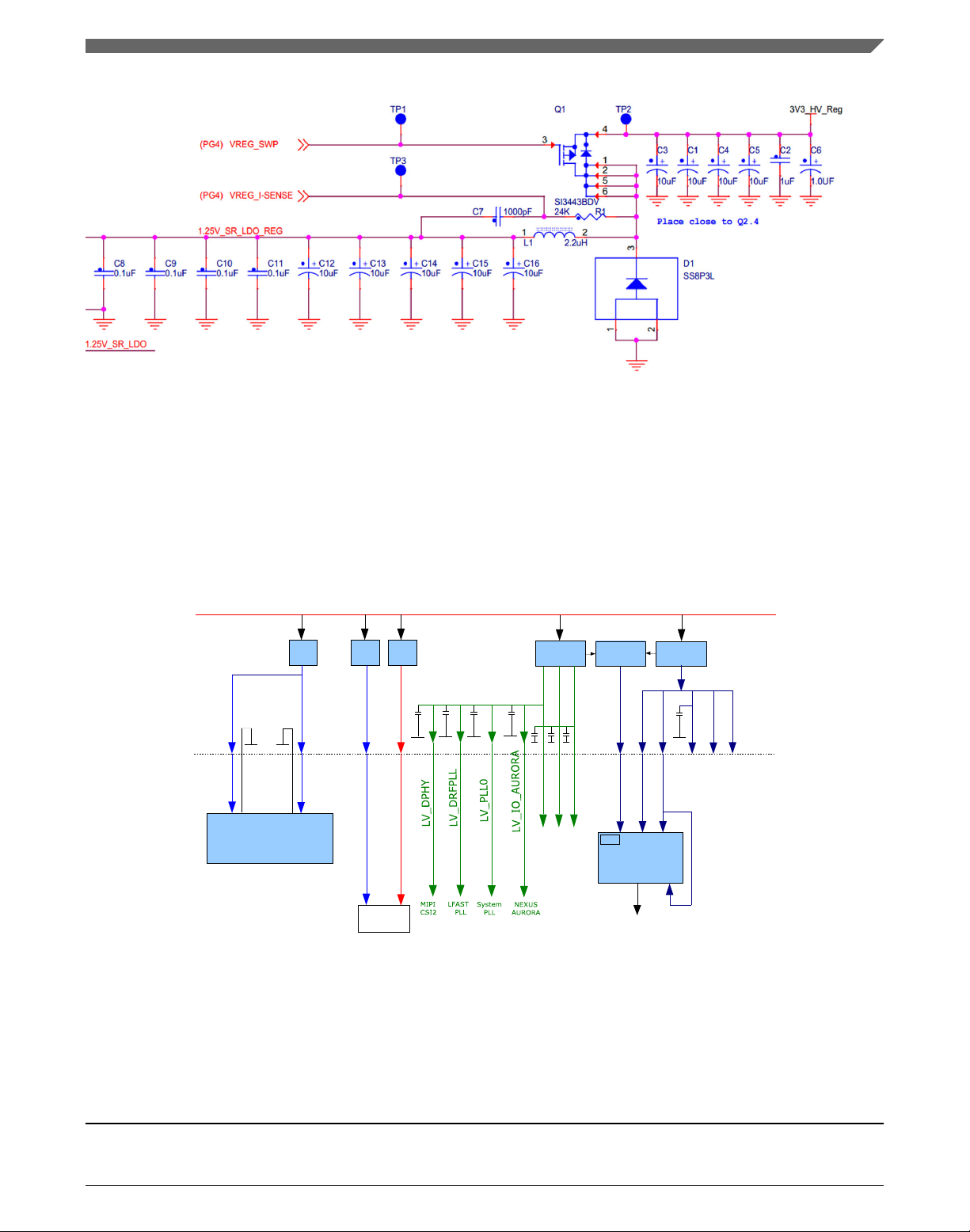
Figure 3. SMPS external components layout
Table 8 provides recommended values for the external components.
Table 8. External component values
Component Label Recommended Value
M1 SI3443, 2SQ2315
L1 2.2 μH 3A <100 mΩ series resistance (E.g. Bourns SRU8043-2R2Y)
D1 SS8P3L 8A Schottcky diode
R1 24 kΩ
C1 10 μF ceramic
Table continues on the next page...
S32R27/37 Hardware Design Guide, Rev. 1, 04/2018
NXP Semiconductors 9
Page 10
Power supply
Table 8. External component values (continued)
Component Label Recommended Value
C2 100 nF ceramic
C3 100 nF ceramic (place close to inductor)
C4 10 μF ceramic (place close to inductor)
C5 1 nF ceramic
C6 4x 100 nF + 4x 10 nF ceramic (place close to MCU supply pins)
C7 4x 10 μF ceramic (place close to MCU supply pins)
C8 100 nF ceramic (place close to MCU supply pins)
C9 1 μF ceramic (place close to MCU supply pins)
1. These are the same capacitors as those listed for VDD_LV_CORE in Table 2
For optimum electro-magnetic interference (EMI) performance, it is critical that the inner and outer loops shown in Figure 3
overlap on the PCB and are made as short as possible. It is highly recommended to have a section of the PCB ground plane
dedicated to making a good connection between the grounds of C1/C2 and C3/C4. This measure will help to ensure that the
loops are made as short as possible.
The role of C1/C2 is to guarantee a low input impedance to the buck converter. In a similar manner, C3/C4 make the
impedance low at the buck converter output. This measure helps reduce the high frequency content of the current passing
through the highlighted branch 'Iload', making it less critical that the buck converter components be placed close to the
VDD/VSS pins of the MCU. However, it is important that capacitors C6 and C7 are placed as closely as possible to the
VDD/VSS pins of the MCU, as they guarantee the low impedance of the core MCU supply and also help to reduce the high
frequency content of the 'Iload' path.
1
The gate-driver circuitry also forms important current loops that must be minimized (not shown in Figure 3). For that
purpose, C8/C9 must be placed as close as possible to the gate-driver supply pins. The ground connections for C8/C9 must be
made as short as possible to C1/C2. When the PMOS switch is turned on, the high-frequency current that charges the gate
comes from C1/C2, passing through the PMOS gate into the gate-driver pin. That current is carried to the gate-driver VSS pin
returning to C1/C2. This current loop must be made as small as possible.
Conversely, when the PMOS switch is turned off, high-frequency currents enter in the PMOS gate coming from the gatedriver pin and flows into C1/C2, returning through the ground into C8/C9 and then into the gate-driver supply pin.
Minimizing this second loop area is as critical as the first.
To shield nearby nets from the gate-driver generated noise, it is also recommended that the gate-driver supply pins are used
to shield the VREG_SWP net until it reaches the PMOS switch. Nets on other PCB layer should avoid running parallel to this
net.
The figure below is a circuit schematic showing an example SMPS circuit derived from the above guidelines. For best
performance, use the component values recommended in Table 8.
S32R27/37 Hardware Design Guide, Rev. 1, 04/2018
10 NXP Semiconductors
Page 11
DC-DC
VReg
Board supply 5V -12V
SAR ADC
3.3V
low noise
POR
Lin.
VReg
3.3V
low noise
Lin.
VReg
Lin.
VReg
POR_B
DC-DC
VReg
AFE
Internal Lin. VRegs
3.3V
low noise
HV_PMU
3.3V
HV_REG_3V8
HV_ADCREF0/2
HV_ADC
1.25V
HV_DAC
HV_RAW
DC-DC
VReg
HV_FLA
HV_IOx
LV_CORE
1.25V, 1.8A
HV_IO_PWM
External
Monitor
Power supply
Figure 4. Example schematic of SMPS external components
3.3.4 External supply mode
If there is a stable 1.25 V regulated supply available to provide the digital low voltage, the internal voltage regulator can be
disabled. This also negates the need for the external SMPS circuit. An overview of the power connections required for such a
configuration is shown in Figure 5. This is the default and only configuration for the S32R372 141MAPBGA packaged
device, due to the reduced pin count.
This mode of operation can be selected by driving the VREG_SEL pin low.8 This disables the internal:
• Voltage regulator (VREG)
• VDD_LV POR function (can be enabled by software)
• VDD_LV LVD/HVD circuits (can be enabled by software)
8. Not required on S32R372 141MAPBGA package as VREG_SEL is internally bonded to GND
NXP Semiconductors 11
Figure 5. Supply connections
S32R27/37 Hardware Design Guide, Rev. 1, 04/2018
Page 12

Power supply
When internal regulation is disabled, the signals VREG_ISENS and VREG_SWP are not needed as they are for feedback and
control of the SMPS circuitry. VREG_ISENS should be connected to VDD_LV_CORE and VREG_SWP is internally pulled
up, so should be left floating.
In external regulation mode, the supply for the internal voltage regulator, VDD_HV_REG3V8, can be connected to the same
supply voltage as VDD_HV_PMU.
Use a single Linear VREG to supply both VDD_HV_RAW and VDD_HV_DAC. Both supply pins must have the
recommended filtering as described in Table 5 and have separate routes (star route) of roughly equal length to the Linear
VREG.
VDD_HV_IO, VDD_HV_IO_RGMII, VDD_HV_IO_PWM and VDD_HV_IO_LFAST supplies should be treated as a
single supply from a board perspective.
VDD_LV POR and LVD/HVD is the responsibility of the external regulation circuit. The device must be kept in reset
(VREG_POR_B driven low) during power-up until all supplies have reached their minimum operating threshold and also
during operation if any of the supplies move outside the specified range, as defined in the device data sheet. To achieve this,
external LVD/HVD circuits are needed to monitor the supplies. After power-up, the internal LVDs/HVDs can be enabled by
software to act as a second tier of detection and provide power supply information to the software.
9
3.4
The S32R family has the capability to monitor selected supply voltages internally. This section concerns only with the
internal monitoring functions for POR and LVD/HVD. The external POR and LVD/HVD circuit behavior will vary and
should be designed using the device data sheet as reference. From this point, it is assumed that internal regulation mode is
being used unless where explicitly stated. In external regulation mode, the internal POR and LVD/HVD are disabled by
default but can be enabled by software after power-up.
The function of the POR and LVD circuits is to hold the device in reset as long as the supply voltages to the LVD circuits are
below the minimum operating voltage. The device is held in reset until the point at which the supplies cross the lower
threshold and the POR and LVDs are released.
3.4.1
The internal LVD and HVD circuits monitor whether the voltage on the corresponding supply is below or above defined
values and either assert a reset or an interrupt. The LVDs/HVDs also support hysteresis for the falling and rising trip points.
Although there is an option to disable the LVDs and HVDs following reset, they are capable of being used in a ‘monitor’
only mode and are also capable of generating a safe/interrupt event. The LVDs/HVDs can also be configured after device
initialization to prevent reset when a supply crosses the LVD threshold, providing a higher voltage range. An application then
must verify the device remains in the functional range.
Supply monitoring
Behavior of LVD / HVD
NOTE
The LVDs that form the power-on reset functionality, monitoring VDD_LV_CORE and
VDD_HV_PMU, cannot be disabled. These modules are used during power-up phase and
must ensure that an absolute lowest threshold of operation is never crossed. This is not a
guarantee that the device will function down to this level. It is rather a guarantee that the
device will recover if this level is crossed.
9. Not required on S32R372 141MAPBGA package as these signals are internally bonded.
S32R27/37 Hardware Design Guide, Rev. 1, 04/2018
12 NXP Semiconductors
Page 13

Power supply
3.4.2 Low-Voltage (LVD) and High-Voltage Detection (HVD)
The internal LVD circuits monitor whether the voltage on the corresponding supply is below defined values and either assert
a reset or an interrupt, while the HVD circuits monitor to ensure a supply does not exceed an upper voltage limit. The LVDs/
HVDs also support hysteresis in the falling and rising trip points.
• All LVDs and HVDs are capable of generating either a reset or an interrupt based on configuration, with the exception
of two POR threshold monitors
• LVD monitoring the internal core voltage (VDD_LV_CORE) always generates a reset when triggered.
• LVD monitoring the PMC voltage supply input (VDD_HV_PMU) always generates a reset when triggered.
• All LVDs and HVDs configured for reset generation cause functional or destructive reset. Reset is not exited until all
destructive reset conditions are cleared.
• The appropriate bits in the PMC status registers are set by LVD and HVD events.
• LVD and HVD control is protected by the SoC-wide register protection scheme. Therefore, it is configurable as long as
the scheme is followed.
• There are user option bits available to allow degrading of “configurable” LVDs/HVDs from destructive down to
functional reset. This is a write once mechanism managed by SSCM during device initialization.
• When the LVD or the HVD is enabled for destructive reset generation, then when a trigger event is detected, the
external RESET_B pin is driven low.
Please refer to the device data sheet for LVD and HVD characteristics.
10
:
3.4.3 Power-on reset
The power management controller (PMC) controls the internal power-on reset (POR) signal for the MCU. POR is the
combination of all internal POR signals from the analog PMC block. When the critical power supplies are below minimum
levels (internal regulation mode) or the VREG_POR_B pin is driven low, the MCU is held in the POWERUP phase of the
reset state machine, POR asserted, until the power supplies have reached specified levels. When the required voltage levels
are reached, POR is deasserted and is input to the reset generation module (MC_RGM) which propagates the device through
the next steps of the boot process.
The PMC has internal POR low voltage detect (LVD) circuits to detect the minimum critical power supply voltages required
to operate the internal voltage regulator, including hysteresis. It monitors:
• The voltage on the 1.25 V supply input, VDD_LV_CORE
• The 3.3 V signal used internally by the PMC, VDD_HV_PMU
Once both these supply voltages are above the threshold the internal POR signal will deassert. See Device reset configuration
and the Reset chapter in the reference manual for VREG_POR_B and RESET_B pin functionality.
3.5
The device is considered to be in a power sequence (POWER-UP state) when the device is either not supplied or is partially
supplied. An internal power-on reset (POR) signal is used to identify POWER-UP state. This signal is released on exit of the
power sequence. The power-on reset signal is a combination of LVD monitoring of the VDD_LV_CORE and
VDD_HV_PMU supplies. The exit from the next phase, PHASE0, depends on the release of the secondary LVD/HVD
circuits, which monitor:
Power sequence
• VDD_LV_PLL0
• VDD_HV_IO
• VDD_HV_FLA
• VDD_HV_ADC
10. As mentioned previously, the internal POR management is disabled by default when external regulation mode is
selected. They cannot be disabled when operating in internal VREG mode.
S32R27/37 Hardware Design Guide, Rev. 1, 04/2018
NXP Semiconductors 13
Page 14

Power supply
Once they have reached the minimum operating threshold the device will exit reset. For more information on phases of the
reset process, please refer to the Reset chapter in the device reference manual.
The actual threshold use for each internal LVD depends on the configuration of the device. This is configurable by hardware
(flash option bits content) or by software (LVD event configuration through PMC register interface). Once the power-on
signal has been asserted, the device configuration is reset to default power-up configuration. During the initialization phase,
the device defaults to a pre-determined state for each of the LVDs, HVDs, and the internal regulators. As the flash memory
becomes available, the differential read process allows the trimmed data to be available for trimming the internal LVDs,
HVDs, and regulators.
3.5.1 Power-up sequence
In this section, the assumption is made that all supplies are low when entering the power-up sequence. Brown-out and power
down sequences are specified in further sections below.
There are simple power sequencing rules to follow in order to correctly power-up the device:
• The system PLL supply (VDD_LV_PLL0) and the core supply (VDD_LV_CORE) must be powered simultaneously. It
is recommended to connect them to the same voltage supply.
• The high-voltage I/O supply (VDD_HV_IO) and the Power Management Unit supply (VDD_HV_PMU) must be
powered simultaneously or VDD_HV_IO ramped before VDD_HV_PMU such that the two supplies always maintain
less than 100 mV difference during the power ramp. They can be connected to the same voltage supply.
• If VDD_HV_DAC and VDD_HV_RAW are supplied by 2 separate regulators, the following must be met:
• For RAW or DAC ramp rates less than 1ms, VDD_HV_DAC comes on no earlier than 500 us before
VDD_HV_RAW.
• for RAW or DAC ramp rates greater than 1ms, VDD_HV_DAC is below 2.0V at the time VDD_HV_RAW
reaches 1.0 V.
• Alternatively VDD_HV_DAC and VDD_HV_RAW can be supplied from the same regulator, providing adequate
decoupling is provided as described in Power supply signals and decoupling
• For the S32R274 device the SD ADCs must be powered before a signal is applied to their inputs, to ensure protection
of the input channels from overdrive signal levels. To do this, ramp VDD_HV_RAW supply before applying input to
the SD ADCs.
All power supplies should ramp at slew rates within the ranges recommended in the device data sheet. For recommended
supply groupings for the S32R372 devices please see the device data sheet power sequencing requirements section.
3.5.2
If the threshold of the configurable monitor LVDs is crossed and they are configured to generate a destructive reset, the
device re-enters the PHASE0 phase. The power-down sequence is started and the device enters the POWER-UP state as soon
as the threshold of one of the POR LVDs (monitoring VDD_LV_CORE and VDD_HV_PMU) is crossed. The device
supplies may then proceed to drop down to ground either through device leakage or external pull-down.
3.5.3
During brown-out, the device re-enters the POWER-UP phase as soon as the threshold of either POR VDD 1.2 V or APOR is
crossed.
Power-down sequence
Brown-out management
S32R27/37 Hardware Design Guide, Rev. 1, 04/2018
14 NXP Semiconductors
Page 15
XOSC
40MHz
1-2ps Jitter
Bypass:
40MHz
FMPLL_1
VCO:600-
1250MHz
IRCOSC
16MHz
Cryst
40MHz
SDPLL
320MHz
IRC_CLK
PLL_CLK0
PLL_CLK1
PLL_0
VCO: 600-
1250MHz
OSC
40MHz
XOSC_CLK
SDPLL_CLK
AFE
XTAL
EXTAL
Clock configuration
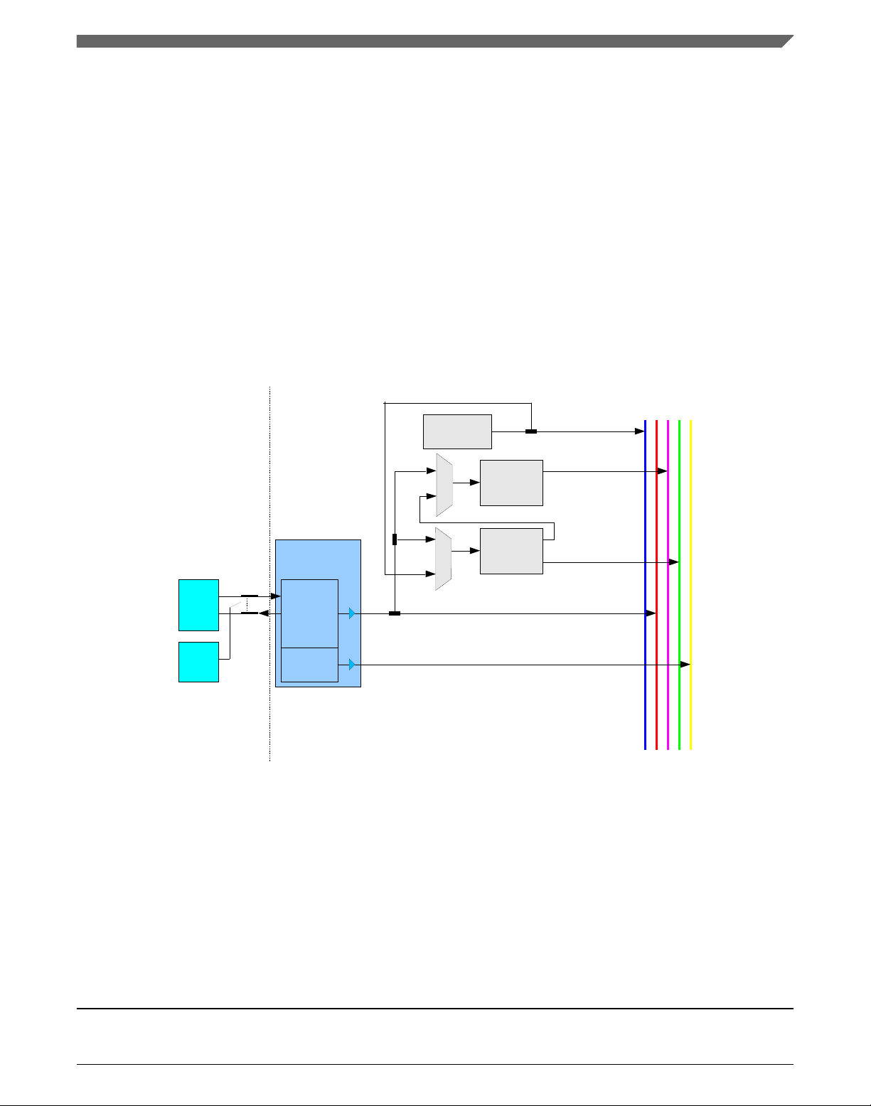
4 Clock configuration
The S32R family system reference clock can be sourced in three ways: using the internal RC oscillator (IRCOSC),
connecting an external crystal or connecting an external oscillator (XOSC). To use XOSC, an external 40 MHz crystal or
oscillator must be connected through the XTAL and EXTAL pins. XTAL and EXTAL pins also support differential LVDS
clock inputs. Information on how to do this can be found in Connecting external clock sources. IRCOSC or XOSC is used as
the clock source for the internal phase-locked loops (PLL) to generate the high frequency clocks for the cores and
peripherals.
This structure provides five different clock domains that are available as the source for system and peripheral clocks:
• IRCOSC - 16 MHz internal reliable RC oscillator
• XOSC - 40 MHz oscillator (using external crystal (XTAL) or external oscillator in bypass (EXTAL))
• PLL0 - up to 240 MHz PLL
• PLL1 - up to 240 MHz frequency-modulated (FM) PLL
• SDPLL- 320 MHz11 PLL for the Sigma-Delta ADC
Figure 6. S32R family clock sources
During power up, the IRCOSC is the default clock for the system. In normal operation, software can then configure each of
the system components to use one of the clock domains as the clock source. The dual PLL must be enabled by software and
can provide separate system and peripheral clocks. PLL0 is the primary PLL driven by the reference clock and used to
provide a clock to the device modules. PLL1 is a frequency-modulated PLL (FMPLL) driven by PLL0 and is used to provide
the system clock. Alternatively, XOSC can be used to drive PLL1.
The most important aspects of an accurate clock source require that some care be taken in the layout and design of the
circuitry around the crystal and PLL power supplies. Any noise in these circuits can affect the accuracy of the clock source to
the PLL. The power supply for the PLL is taken from VDD_LV_PLL0. Noise on this supply can affect the accuracy and
jitter performance of the PLLs. In order to minimize any potential noise, it is recommended that the additional capacitors
recommended in Table 5 are fitted to the VDD_LV_PLL0 supply.
11. Divided by 2 (160 MHz), and 4 (80 MHz) if used for system and peripheral clocks
S32R27/37 Hardware Design Guide, Rev. 1, 04/2018
NXP Semiconductors 15
Page 16

XTAL EXTAL
Crystal
S32R27X / S32R37X
XTAL EXTAL
S32R27X / S32R37X
40MHz
Clock
Clock configuration
4.1 Connecting external clock sources
The S32R family features internal load capacitance on the XTAL and EXTAL pins for connecting external clock sources.
This feature is intended to simplify the design and reduce the overall system cost by eliminating external components and
reducing the PCB footprint. See the device data sheet for details on the internal capacitance values. PCB designers must take
into account the parasitic capacitance levels on the signal lines connecting an external oscillator to the XTAL and EXTAL
pins in order to avoid frequency deviation. Generally, for a crystal with load capacitance of 8 pF, a capacitance figure of 12
pF on the signal lines connected to both XTAL and EXTAL will result in good oscillator performance. Choose a crystal with
a Q factor of > 25,000.
A diagram for the connection of an external 40 MHz crystal oscillator is shown in the figure below.
Figure 7. External oscillator connection
The oscillator should be placed as close as possible to the MCU. In order to minimize signal degradation, the circuitry should
be placed entirely on only one PCB layer, avoiding unnecessary vias where possible. Do not allow any signals to cross the
crystal connections to the device. Absolutely no high current or high speed signals should be run near any of the crystal
components.
Other than the connections shown in the above schematics, no other connections should be made to the crystal or EXTAL
and XTAL device pins. Do not use XTAL to drive any other circuitry than shown.
If an external single clock source is being used as clock reference to the MCU, then the XTAL pin should be left floating and
the clock should be provided to EXTAL as shown in the figure below. Note that the clock source should be a low voltage
signal, please ensure any source meets the specifications detailed in the device data sheet for the input signal to avoid
potential damage to the device.
Figure 8. External clock connection (Single Ended Bypass Mode)
In order to use a differential LVDS clock input for the device, the device offers 100 Ω internal termination resistance between
EXTAL and XTAL pins. For differential operation positive clock should be connected to XTAL and negative to EXTAL
pins, and if the clock is a differential voltage source then AC coupling capacitors of 0.01 uF should be used, as shown in the
figure below. Care should be taken during PCB design to avoid vias, and ensure that all differential pairs are trace and
impedance matched, and also follow differential pair best practices as detailed later in the document.
S32R27/37 Hardware Design Guide, Rev. 1, 04/2018
16 NXP Semiconductors
Page 17

S32R27X / S32R37X
S32R27X / S32R37X
Device reset configuration
Figure 9. External clock connection (Differential LVDS AC Coupled Mode)
Figure 10. External clock connection (Differential LVDS DC Coupled Mode)
Using either of these methods to connect an external clock makes it available as the XOSC internal clock source.
5
Device reset configuration
The S32R family of MCU's require only very basic external reset circuitry. External circuitry for device configuration is not
required. The device is configured during reset based on data in stored flash memory.
5.1
The S32R family of devices feature two active-low external reset signals:
RESET_B is a bidirectional reset input/output that indicates if the device is active (high signal) or in reset. It is thus weak
pull-up after the reset sequence has completed, but an external pull up resistor to VDD_HV_IO should also be used. A falling
edge on this pin will trigger a functional reset to the Reset Generation Module (RGM). Forcing this pin low will keep the
device in the last phase of the reset sequence (Phase3[Functional]).
In external voltage regulation mode, VREG_POR_B allows external supply circuits to signal to the MCU when power is
available, so the power-up sequence can begin. It should be forced high when the critical power supplies cross the LVD
threshold.
External reset signals
• Functional reset (RESET_B)
• Power-on reset (VREG_POR_B)
In internal regulation mode, VREG_POR_B is not needed as the POR is managed within the PMC. It is internally pulled up
to the PMC voltage, so it can be left floating. Alternatively, it can be connected to VDD_HV_PMU through a 4.7 Kilo Ohm
pull-up resistor.
Both of these pins operate on the 3.3 V power domain.
12. Note that
reset in the device.
NXP Semiconductors 17
, 12
VREG_POR_B remains active in internal regulation mode. As such, if it is pulled low it will cause a power-on
S32R27/37 Hardware Design Guide, Rev. 1, 04/2018
Page 18

Recommended debug connectors and connector pin-out definitions
6 Recommended debug connectors and connector pin-out
definitions
The S32R microcontroller family implements the newly added (in the IEEE-ISTO 5001™-2011 version of the standard) high
speed serial Nexus trace Auxiliary Port that uses the Xilinx™ Aurora physical interface. The Aurora interface allows the
Nexus protocol information to be transmitted serially at a high date rate over one or more Aurora lanes. The Aurora protocol
handles the encoding of the data and stripes the information across the number of lanes available on the device.
Table 9 shows the recommended connectors for different applications for the S32Rxxx Family.
Table 9. Recommended connectors
Connector style Target system part number Connector type
14-pin BERG JTAG only 3M 2514-6002UB JTAG-only configuration
17-position (2 × 17, 34-pin) Samtec Samtec ASP-137973-01 Serial Nexus configuration (supports up
to 8 simplex lanes, less lanes are
available if duplex support or High
Speed Calibration LFAST interface
support is required)
NOTE
Whichever connector is chosen, "keep-out" areas may be required by some tools. Consult
the preferred tool vendor to determine any area that must remain clear around the debug
connector. Some tool vendors may include an extension cable to minimize "keep-out"
areas, but use of an extension will degrade the signal. In many cases, this degradation will
be insignificant, but it depends on many factors including clock frequency and target
board layout.
6.1
Table 10 shows the pinout of the recommended JTAG connector to support the S32R device family.
The recommended connector for the target system is Tyco part number 2514-6002UB.
S32R Family JTAG connector
Table 10. Recommended JTAG connector pinout
Description Pin Pin Description
TDI 1 2 GND/VSS
TDO 3 4 GND/VSS
TCK 5
EVTI0 7 8 VREG_POR_B
RESET_B 9 10 TMS
VREF/VDD 11 12 GND/VSS
EVTO0 13 14 JCOMP
1
6 GND/VSS
1. If LBIST is enabled, an external pull resistor between 1 Kilo and 100 Kilo Ohm must be connected between TCK and either
VDD/VSS to avoid LBIST failures
S32R27/37 Hardware Design Guide, Rev. 1, 04/2018
18 NXP Semiconductors
Page 19

Recommended debug connectors and connector pin-out definitions
Figure 11. Diagram of the JTAG connector pinout
6.2
For high speed Nexus Aurora trace applications, the Samtec™ ERF8 Series connector is recommended in the IEEE-ISTO
5001™-2011 standard. For the S32R family, the 17 position (34 pins) connector is recommended. The part number of the
Samtec connectors are shown in Table 11.
S32R family high-speed Nexus serial trace connector
Table 11. Recommended high-speed serial trace connector part numbers
Connector Part number (Samtec) Style Description
HS34 ASP-137973-01 Samtec ERF8 Series, 17
position by 2 row
HS34 ASP-177706-02 Samtec ERF8 Series, 17
position by 2 row
The Samtec ERF8 series of connectors is intended for high speed applications requiring a minimum footprint size with a
reliable, latching connection. The recommended connector has two rows of seventeen contacts each with a spacing of 0.8
mm. The connector provides isolation between the high-speed trace signals and the low-speed JTAG and control signals. It
also provides ample ground connections to ensure signal integrity. If at all possible, the connector should be placed onto the
target system with the even numbered pins nearest the edge of the printed circuit board. It is also recommended that the
"even" side of the connector be mounted closer to the edge of the printed circuit board to facilitate a direct connection to the
tool.
Figure 12 is courtesy of Samtec U.S.A.
Vertical mount for MCU
module
Right Angle mount for MCU
module
S32R27/37 Hardware Design Guide, Rev. 1, 04/2018
NXP Semiconductors 19
Page 20

Recommended debug connectors and connector pin-out definitions
Figure 12. Recommended Nexus connector
Table 12 shows the recommended pinout for the Samtec connector.
Table 12. S32R family high-speed serial trace connector
Function Pin No Pin No Function
TX0+ 1 2 VREF
TX0- 3 4 TCK/TCKC/DRCLK
VSS 5 6 TMS/TMSC/TxDataP
TX1+ 7 8 TDI/TxDataN
TX1- 9 10 TDO/RxDataP
VSS 11 12 JCOMP/RxDataN
TX2+ 13 14 EVTI1
TX2- 15 16 EVTI0
VSS 17 18 EVTO0
TX3+ 19 20 VREG_POR_B
TX3- 21 22 RESET_B
VSS 23 24 VSS
1
(TX4+)
1
(TX4-)
VSS 29 30 VSS
1
(TX5+)
1
(TX5-)
VSS GND GND VSS
25 26 CLK+
27 28 CLK-
31 32 EVTO1/RDY
33 34 N/C
1. Reserved for TXn signals, not currently used.
S32R27/37 Hardware Design Guide, Rev. 1, 04/2018
20 NXP Semiconductors
Page 21

+
–
+
–
Clock
transmitter
100 Ω
On-chip
receiver
In target
system
+
–
+
–
Tool
+
–
+
–
Aurora
receiver
Aurora
transmitter
Two to four Aurora
lanes are supported.
On-chip
circuitry
100 pF
100 pF
100 Ω
100 Ω
Recommended debug connectors and connector pin-out definitions
6.3 Nexus Aurora target system requirements
The Nexus Aurora interface requires termination and AC coupling of the signals between the target system and the tool. The
termination resistor for the Aurora clock is located inside the MCU. An external termination resistor is required. The transmit
termination resistor must be implemented in the target system; however, it may be implemented internal to the FPGA of the
tool.
Figure 13. Nexus Aurora termination and coupling circuits
6.4
Next to the connector, additional circuitry is required for the Nexus/JTAG debug circuitry. The S32Rxxx devices include
internal pull devices that ensure the pins remain in a safe state. However, if there is additional circuitry connected to the
Nexus/JTAG pins, or long traces that could be affected by other signals (due to crosstalk from high-current or high-speed
signals), a minimum number of external pull resistors can be added to ensure proper operation under all conditions.
Minimum external circuitry
Table 13. Optional external pullups/downs
Nexus/JTAG signal Resistor/capacitor direction and
value
JCOMP 4.7 kΩ pulldown Holds debug port in reset and prevents
VREG_POR_B 4.7 kΩ pullup See External reset signals for details
RESET_B 4.7 kΩ pullup See External reset signals for details
Nexus CLKP & CLKN 10 pF on the signal lines The LVDS Nexus clock signals require a
any debug commands from interfering
with the normal operation of the MCU
capacitor for high speed functionality
EVTI 4.7 kΩ pullup A pullup resistor prevents debug mode
from being forced after reset if debug
mode is enabled (JCOMP = high). It also
prevents breakpoints from being forced if
debug mode is enabled.
Description
NXP Semiconductors 21
S32R27/37 Hardware Design Guide, Rev. 1, 04/2018
Page 22

ADC overview
Table 13. Optional external pullups/downs
Nexus/JTAG signal Resistor/capacitor direction and
value
NOTE:
In addition to the pullup and pulldown resistors, some systems may want to use buffers between the JTAG connector inputs
(JCOMP, TDI, TDO, TMS, EVTI, EVTO, VREG_POR_B, and RESET_B) and the MCU. This will prevent over-voltage
conditions from causing damage to the MCU signals. Normal systems should not require this circuitry, but it is helpful in
systems that can be exposed to improper connections that provide voltages that are outside the operating conditions of the
MCU. A common circuit to use is the Texas Instruments™ SN74CBTLV38615. This device is a bus switch that implements
a bidirectional interface between two terminals with less than 5 Ω of resistance. It should be powered by the same supply that
powers the debug port. The device enable should be connected to ground for the interface to be enabled whenever the debug
port on the MCU is powered. This circuit provides a high impedance to the tool when the debug port is powered off.
7
ADC overview
The S32R274 has two types of analog-to-digital converters (ADCs) that are designed for different applications:
• Two 12-bit Successive-Approximation-Register (SAR) ADCs with a configurable number of channels (up to 16 each)
for voltage and temperature monitoring among other general applications
• Four 12-bit Sigma-Delta (SD) ADC instances for rapid RADAR signal conversions
Description
In almost all situations, a
resistor is not required on this
signal.
The S32R372 device also has two 12-bit SAR ADCs with a configurable number of channels (up to 16 each), but does not
have any SDADC instances.
The SDADC (where applicable) is part of the RADAR analog front-end and is detailed in Sigma-Delta ADC. This chapter
will focus on the SAR ADCs.
The SAR ADCs receive input from 16 multiplexed pins. Please refer to the Power supply section for information on how to
connect the ADC power and reference pins.
Each ADC instance receives input from a number of pins (channels), some of which are multiplexed to share with other ADC
instances. This multiplexing, along with many other attributes of the ADCs, is controlled by configuration registers. Each
ADC instance has an interface to the DMA controller for retrieval of converted data, the FCCU for error handling and the
interrupt controller. Conversions can be triggered by hardware, software or externally:
• A Cross triggering unit (CTU) connected to each ADC allows automatic generation of ADC conversion requests on
user selected conditions without CPU involvement.
• eTimer module provides the capability for external trigger injection to request a conversion.
• The CPU can request a conversion through software
7.1
On the S32R family 257MAPBGA packages there are 16 external analog pins and on the S32R372 141MAPBGA package
there are 6 external analog pins, that act as input channels for the SAR ADCs. They are multiplexed in order to facilitate
sharing of the pins among the ADC instances.
SAR analog input pin multiplexing
There is an analog bypass bit "APC" in the Multiplexed Signal Configuration Register (MCSR) registers of the System
Integration Unit (SIUL2) for the pins to disable the digital circuitry from the analog pins.
S32R27/37 Hardware Design Guide, Rev. 1, 04/2018
22 NXP Semiconductors
Page 23

Table 14 gives the analog input pin assignment for the S32R family packages.
Table 14. ADC pin muxing
RADAR analog front end
Channel Number ADC_0 S32R274
and
S32R372
257MAPB
GA PAD
Channel 0 PB[7](GPIO_23) M3 - PB[13]
Channel 1 PB[8]
(GPIO_24)
Channel 2 PC[1]
(GPIO_33)
Channel 3 PC[2]
(GPIO_34)
Channel 4 PE[6]
(GPIO_70)
Channel 5 PE[2]
(GPIO_66)
Channel 6 PE[7]
(GPIO_71)
Channel 7 PE[4]
(GPIO_68)
Channel 8 PE[5]
(GPIO_69)
Channel 9 PMC_to_ADC - - - - - Internal
Channel 10 Bandgap
Reference PMC
Channel 11 PB[9]
(GPIO_25)
Channel 12 PB[10]
(GPIO_26)
Channel 13 PB[11]
(GPIO_27)
Channel 14 PB[12]
(GPIO_28)
Channel 15 TSENS0 - - TSENS1 - - Internal
N1 - PB[14]
N3 - PB[15]
P1 - PC[0]
M4 K2 - - - External
R1 L2 - - - External
T1 - - - - External
P3 L1 - - - External
R2 - - - - External
- - Bandgap
T3 - PB[9]
R3 - PB[10]
T2 - PB[11]
U2 - PB[12]
S32R372
141MAPB
GA PAD
ADC_1 S32R274
(GPIO_29)
(GPIO_30)
(GPIO_31)
(GPIO_32)
Reference PMC
(GPIO_25)
(GPIO_26)
(GPIO_27)
(GPIO_28)
S32R372
and
S32R372
257MAPB
GA PAD
J4 H3 External
L1 - External
K4 H2 External
L2 J3 External
- - Internal
T3 - External
R3 - External
T2 - External
U2 - External
141MAPB
GA PAD
Channel Type
8 RADAR analog front end
The S32R microcontroller family integrates a number of high-performance digital and analog subsystems to support the
implementation of next-generation RADAR-based advanced driver assistance systems. The analog front-end (AFE) module
acts as an interface to the control registers for use with the integrated analog hard block, which includes:
• Sigma-delta PLL (SDPLL) producing 320 MHz/160 MHz/80 MHz clocks for AFE components
• Low phase noise, low (1-2ps) jitter 40 MHz oscillator (XOSC)
S32R27/37 Hardware Design Guide, Rev. 1, 04/2018
NXP Semiconductors 23
Page 24

Filtered Output
Bus Interface
Decimation
Filters x4
Modulator
Output
x4
14 bits x4
Conversion
Complete x4
Control
Registers
Interrupts
A/D Input
Pairs x4
Crystal
Interface
DAC
Output
Pair
Powers,
Grounds,
Tank
Capacitors
Filter Enables
DAC Data
Clock
Generation
AFE Analog Block
SDPLL Output
320 MHz, 160 MHz,
80 MHz clocks
IPS
RADAR analog front end
The S32R27X AFE also contains:
• Four continuous time sigma-delta ADCs (SDADC)
• 12-bit high accuracy digital-to-analog converter (DAC)
A diagram of the AFE structure is shown in Figure 14. To support the high accuracy, high dynamic range analog
functionality of the above features, careful configuration of power supplies and external circuitry is required to preserve
signal integrity.
24 NXP Semiconductors
Figure 14. AFE Wrapper block diagram
S32R27/37 Hardware Design Guide, Rev. 1, 04/2018
Page 25

RADAR analog front end
8.1 AFE power supplies and external connections
The AFE module requires multiple external connections. These are a mixture of high-fidelity analog power supplies, digital
power supplies, ground connections, external capacitor connections and output signals for the various functions.
Table 15. AFE power supply connections
Name Voltage
Range
VDD_HV_RAW 3.13 V - 3.6 V 3.3 V Connects to 1.4 V regulators for: XOSC, SD PLL and SD
VDD_HV_DAC 3.13 V - 3.6 V 3.3 V Connects to DAC regulator
Domain Function
ADC analog and digital.
The table below shows the pins that the AFE exposes for the connection of external components. The components should be
connected between the pin and ground.
Table 16. AFE external component connections
Pin Name Function Recommended
SD_R External 0.1% trimming resistor for
tuning the ADC resistor array.
VDD_LV_SDCLK External bypass capacitor for LVDS
analog 1.4 V VREG.
VDD_LV_OSC External bypass capacitor for XOSC
analog 1.4 V VREG
VDD_LV_SDPLL External bypass capacitor for SD PLL
analog 1.4 V VREG.
VDD_LV_RADARREF External bypass capacitor for 1.2 V from
the VREF.
DAC_C DAC connection to external cap for
noise filtering.
SD_CM ADC common mode external bypass
capacitor
VDD_LV_SDADC External bypass capacitor for ADC
analog 1.4 V Vreg.
VDD_LV_RADARDIG External bypass capacitor for ADC
digital 1.4 V Vreg.
AFE_FILTER Bypass capacitor for filtered analog
supply
VDD_LV_DAC2V5 Bypass capacitor rampDAC 2.5 V VREG 1.0 μF & 0.1 μF grounded to
40.2 Kilo Ohm +/-0.1%
1.0 μF & 0.1 μF grounded to
VSS_LV_SDCLK
1.0 μF & 0.1 μF grounded to
VSS_LV_OSC
1.0 μF & 0.1 μF grounded to
VSS_LV_SDPLL
1.0 μF grounded to VSS_LV_SDADC
10 μF connected to VDD_HV_DAC
1.0 μF & 0.1 μF grounded to
VSS_LV_SDADC
0.47 μF & 0.1 μF grounded to
VSS_LV_SDADC
1.0 μF & 0.1 μF grounded to
VSS_LV_RADARDIG
1.0 μF & 0.1 μF grounded to
VSS_LV_SDADC
VSS_HV_REGDAC
8.2 Sigma-Delta ADC
The four time-continuous SD ADCs receive input as a differential pair. Each instance has two dedicated input pins.
S32R27/37 Hardware Design Guide, Rev. 1, 04/2018
NXP Semiconductors 25
Page 26

RADAR analog front end
Table 17. Sigma-Delta ADC external connections
Name Pin
(257MBGA)
SD_0_ADCN A1 I ADC0 negative input
SD_1_ADCN A2 I ADC1 negative input
SD_2_ADCN A3 I ADC2 negative input
SD_3_ADCN A4 I ADC3 negative input
SD_0_ADCP B1 I ADC0 positive input
SD_1_ADCP B2 I ADC1 positive input
SD_2_ADCP B3 I ADC2 positive input
SD_3_ADCP B4 I ADC3 positive input
AC coupling capacitors should be used at the SD ADC inputs in order to remove any DC bias present and allow the AC
signal to pass through. This ensures that the ADC's operate within their input range. The recommended value for these
capacitors is 0.22μF, as shown in Figure 15.
Direction Function
Figure 15. SD ADC AC coupling capacitors
8.3
The DAC is used to produce analog ramp signals for generation of RADAR waveforms.
Digital-to-Analog Converter
Table 18. DAC signal description
Name Pin (257MBGA) Direction Function
DAC_AN C8 O DAC negative output (current)
Connected to external 300
Ohm resistor
Table continues on the next page...
S32R27/37 Hardware Design Guide, Rev. 1, 04/2018
26 NXP Semiconductors
Page 27

S32R274
DAC_AP
DAC_AN
300 Ohm
300 Ohm
RADAR analog front end
Table 18. DAC signal description (continued)
Name Pin (257MBGA) Direction Function
DAC_AP C7 O DAC positive output (current)
Connected to external 300
Ohm resistor
The resistors are required because the DAC output is a current source. Figure 16 shows how to connect the external resistors
to the DAC output pins.
8.4
There are no external connections required for the Sigma-Delta PLL. Information on configuration can be found in the
Analog Front End chapter in the device reference manual.
8.5
Instructions on how to connect an external source to drive the XOSC clock can be found in Connecting external clock
sources.
XOSC_EXTAL F1 C1 I EXTAL analog input
XOSC_XTAL E1 D1 O XTAL analog output
Figure 16. DAC Output Pin Connections
Sigma-Delta PLL
XOSC
Table 19. XOSC external connections
Name Pin (257MBGA) Pin (141BGA) Direction Function
signal
signal
S32R27/37 Hardware Design Guide, Rev. 1, 04/2018
NXP Semiconductors 27
Page 28

RADAR analog front end
8.6 AFE pin configuration when not using on-board ADC's and DAC
For an application which utilizes the MIPI-CSI2 interface to provide raw ADC data to the S32R274 device the unused pads
for the on board SD-ADC's and DAC, along with associated supplies must be configured as shown in Table 20 to ensure safe
operation of the device. These connections also apply to the S32R372 257 MAPBGA package since this is pin compatible
and does not contain the on-board ADC's.
Table 20. AFE Pin Requirements when using off-chip ADC/DAC
Pin Number Pin Name Requirement
A1 SD_0_ADCN Connect to SD_0_ADCP and leave floating (or N.C for S32R372)
A2 SD_1_ADCN Connect to SD_1_ADCP and leave floating (or N.C for S32R372)
A3 SD_2_ADCN Connect to SD_2_ADCP and leave floating (or N.C for S32R372)
A4 SD_3_ADCN Connect to SD_3_ADCP and leave floating (or N.C for S32R372)
B1 SD_0_ADCP Connect to SD_0_ADCN and leave floating (or N.C for S32R372)
B2 SD_1_ADCP Connect to SD_1_ADCN and leave floating (or N.C for S32R372)
B3 SD_2_ADCP Connect to SD_2_ADCN and leave floating (or N.C for S32R372)
B4 SD_3_ADCP Connect to SD_3_ADCN and leave floating (or N.C for S32R372)
C1 SD_CM 1 μF Capacitor to Ground
C2 SD_R Can be relaxed to 40k-47k Ohm +/- 10%
C5 DAC_C Not used, leave floating
C7 DAC_AP Not used, leave floating
C8 DAC_AN Not used, leave floating
D4 AFE_FILTER 0.1 & 1 μF Capacitor to Ground
C3 VDD_LV_RADARREF 1uF Capacitor to Ground
D1 VDD_HV_RAW 3.3 V
D2 VSS_HV_RAW Tied to Ground
D8 VDD_HV_DAC 3.3 V
D7 VSS_HV_DAC Tied to Ground
E4 VDD_LV_SDADC 0.47 μF Capacitor to Ground
C4 VSS_LV_SDADC Tied to Ground
D3 VDD_LV_RADARDIG 1 μF Capacitor to Ground
E3 VSS_LV_RADARDIG Tied to Ground
F3 VDD_LV_OSC 0.1 & 1 μF Capacitor to Ground
F2 VSS_LV_OSC Tied to Ground
E1 XOSC_XTAL Differential clock supplied from external differential source + or F1 XOSC_EXTAL Differential clock supplied from external differential source - or +
E2 VDD_LV_SDPLL 0.1 & 1 μF Capacitor to Ground
F4 VSS_LV_SDPLL Tied to Ground
G3 VDD_LV_SDCLK 0.1 & 1 μF Capacitor to Ground
G4 VSS_LV_SDCLK Tied to Ground
Table continues on the next page...
S32R27/37 Hardware Design Guide, Rev. 1, 04/2018
28 NXP Semiconductors
Page 29

+
0.47uF
+
0.1uF
3.3V or 5V
1
6
2
7
3
8
4
9
5
DB9F
FB
1
V+
C1-
C2+
C2-
V-
DOUT2
8
Vcc
16
GND
15
DOUT1
RIN1 ROUT1
DIN1
DIN2
ROUT2
0.1uF
SCI_TXDA
SCI_RXDA
MAX3232
SCI_RXDA2
HOST-R2
SCI_TXDA2
HOST-T2
9
HOST-R1
HOST-T1
+
0.47uF
+
0.47uF
+
10
11
12
7
RIN2
14
13
2
4
C1+
3
6
5
Example communication peripheral connections
Table 20. AFE Pin Requirements when using off-chip ADC/DAC (continued)
C6 VDD_HV_DAC_2V5 1 μF Capacitor to Ground
D5 VSS_HV_REGDAC Tied to Ground
H3 VSS_SUB_INPWB0 Tied to Ground
D6 VSS_SUB_INPWB1 Tied to Ground
H4 VSS_SUB_OUTPWB Tied to Ground
9 Example communication peripheral connections
There are a wide range of peripheral pins available on the MCU. Many of these have fairly standard definitions for their use.
This section provides example connections for some of the most commonly used communications peripherals, such as LIN,
FlexCAN, FlexRay, and RS-232 communication interfaces.
9.1
Example RS232 interface
The RS-232 (TIA/EIA-232-F) standard is a fairly common interface that is available on all computers. While this interface is
disappearing, adapters are available to allow the use of RS-232 peripherals through other interfaces, such as USB. RS-232
was intended to be a very low-cost and low-performance interface. This interface was originally specified with signal
voltages of +12 V and –12 V, typically. However, this has been lowered to a typical minimum voltage of +5 V and –5 V in
recent years.
Figure 17 and Table 21 show the typical connections between the serial port of an MCU and the MAX3232-EP RS-232D
transceiver from Texas Instruments http://www.ti.com/. The transceiver operates from either a 3.3 V or a 5 V supply and
includes two charge pumps to generate the output voltages that are required. This device contains two transmit drivers and
two receivers. The charge pumps require four external capacitors.
NXP Semiconductors 29
Figure 17. Typical SCI to RS232 circuit
S32R27/37 Hardware Design Guide, Rev. 1, 04/2018
Page 30

Example communication peripheral connections
The commercial grade MAX3232 device is not rated for the full automotive temperature
of -40 to +125° C and is not intended for automotive applications. This circuit should not
be used or populated in a production module intended for automotive use. However, in
many cases, the RS-232 interface is intended only as a development interface; therefore,
the commercial device can be used for prototyping purposes. Texas Instruments does
offer a device option with an operating temperature range of -40 to +85° C. Texas
Instruments has an enhanced version of the device, MAX3232-EP, that is intended for
aerospace, medical, and defense applications. This version is available with an operating
temperature range of –55 to +125° C.
Table 21. Typical RS-232D connector definition
Pin number Description
1 Connect to pin 4 and 6
2 RS-232 TX (Transmit)
3 RS-232 RX (Receive)
4 Connect to pin 1 and 6
5 GND
6 Connect to pin 1 and 4
7 N/C
8 N/C
9 N/C
NOTE
NOTE
N/C pins are not connected. The shell of the connector should be connected through a
ferrite bead to ground.
9.2
Local Interconnect Network (LIN) is a commonly used low-speed network interface that consists of a master node
communicating with multiple remote slave nodes. Only a single wire is required for communication and is commonly
included in the vehicle wiring harness. Figure 18 shows a typical interface implemented using the NXP MC33661 LIN
transceiver.
Example LIN interface
S32R27/37 Hardware Design Guide, Rev. 1, 04/2018
30 NXP Semiconductors
Page 31

Control
Receiver
INH
Control
5
GND
7 VSUP
MC33661
LIN Bus
Master Node
Pullup
RXDx
TXDx
VPWR
33K Ω
+5V
10K Ω
GPIO
+5V
Slave Node
12
34
WAKE
WAKE
Master
3
WAKE
2
EN
1
RXD
4
TXD
6
LIN
8
INH
30kΩ
Slope
Control
20 μA
10 μF
1kΩ
Example communication peripheral connections
Figure 18. Typical LIN connections
Table 22 below shows the pins of the MC33661 and their typical connections to an MCU.
Table 22. MC33661 pin definitions and example system connections
Pin number Pin name Pin direction Full pin name MCU or system
1 RXD Output Receive Data
Output
2 EN Input Enable Control MCU GPIO Enables operation
3 Wake Input Wake Input LIN Bus Wake
4 TXD Input Transmit Data Input MCU LIN TXD LIN Transmit Data
5 GND Input Ground System Ground
6 LIN Input/Output LIN Bus LIN bus Bidirectional pin
7 VSUP Input Power Supply Protected battery
Table continues on the next page...
Description
connection
MCU LIN RXD LIN Receive Data
Output to the MCU
of the device
1
Wake enables the
devices out of
sleep mode
Input from the MCU
Device ground
Reference
reference
that represents the
single-wire transmit
and receiver
voltage
This is the power
supply for the
device and is
typically connected
to a nominal 12 V
NXP Semiconductors 31
S32R27/37 Hardware Design Guide, Rev. 1, 04/2018
Page 32

Example communication peripheral connections
Table 22. MC33661 pin definitions and example system connections (continued)
Pin number Pin name Pin direction Full pin name MCU or system
connection
8 INH Output Inhibit Output LIN Bus (if master) The Inhibit pin
1. Wake is an optional signal on the LIN connector, but may come directly from a switch.
Description
controls either an
external regulator
to turn on a slave
node or is
connected through
a resistor to the LIN
bus on master
nodes
There is no standard industry-defined LIN connector. NXP uses a 4-pin Molex® connector that allows for the LIN bus pin, a
power supply source (VPWR), a wakeup signal, and a ground reference. Slave nodes will often implement two connectors to
allow a daisy-chain of multiple nodes to be easily implemented. Table 23 shows the NXP pinout.
Table 23. LIN connector pinout recommendation
Function Pin number Pin number Function
LIN Bus 4 3 VPWR
Wake 2 1 Ground
In a typical system, these pins would be used as follows:
• LIN bus—This is the single-wire LIN bus that connects between the master LIN node and the slave LIN nodes.
• VPWR—This connector input can be used as the power input to a slave node. Care should be taken that sufficient
current is available for the total number of LIN slaves that are powered through this connection. In some systems, this
may come from the master LIN node.
• Wake—The Wake signal is typically used for each individual slave node to enable the LIN physical interface of that
node and to consequently enable the power supply (using the INH output) to power up the MCU to perform some
action. For example, when the handle on a car door is lifted, to turn on the MCU that controls a function inside the
vehicle, such as powering a smart dome light or enabling the controls of a smart seat.
• Ground—Ground reference for the module.
Part numbers for the 4-pin Molex Mini-Fit Jr.™ connector are shown in Table 24.
Table 24. Recommended connector part numbers
Description Manufacturer part number
(Molex)
4-pin right-angle connector with flange for target system, tin contacts, with latch 39-29-1048
4-pin right-angle connector with pegs for target system, tin contacts, with latch 39-30-1040
4-pin vertical connector with pegs for target system, tin contacts, with latch 39-29-9042
4-pin right-angle connector with flange for target system, gold contacts, latch 39-29-5043
Mating connector with latch for cable assemblies 39-01-2040
Socket terminal for mating cable assembly 39-00-0077
S32R27/37 Hardware Design Guide, Rev. 1, 04/2018
32 NXP Semiconductors
Page 33

MCU FR_x_TX
MCU FR_x_TXEN
MCU FR_x_RX
MCU GPIO
MCU_GPIO
BP
BM
Vbatt
+5V
+3.3V
+3.3V
+
10 μF
+
10K
47R
47nF
4700 pF
10K
C21
33pF
C21
33pF
+
10 μF
+
4700pF
47R
++
10 μF
47pF
TJA1080ATS/1
TRXD0
11
TRXD1
10
TXD
5
TXEN
6
BGE
8
STBN
9
EN
3
WAKE
15
INH2
1
INH1
2
BP
18
BM
17
RXD
7
ERRN
13
RXEN
12
VIO
4
VCC
19
VBUF
20
VBAT
14
GND
16
47pF
10K
4700 pF
51μH
21
4 3
10K
Example communication peripheral connections
9.3 Example FlexRay interface
FlexRay is an automotive fault-tolerant 2-wire communications interface. NXP FlexRay devices implement a
Communications System Electrical Physical Layer Specification, Version 2.1 Rev A compliant bus driver interface.
Typically FlexRay bus data rates of 10 Mbit/s, 8 Mbit/s, 5 Mbit/s, and 2.5 Mbit/s are supported and although the logic
portions of the interface are implemented in the device, an external physical interface device is required to allow multiple
FlexRay modules to be connected together.
The NXP™ (http://www.nxp.com ) TJA1080A device is typically used as the FlexRay transceiver, although others are also
available. One transceiver is required for each FlexRay channel. Figure 19 and Table 25 below shows the typical connections
using the TJA1080A.
Figure 19. Typical FlexRay circuit
S32R27/37 Hardware Design Guide, Rev. 1, 04/2018
NXP Semiconductors 33
Page 34

Example communication peripheral connections
Decoupling is shown as an example only. TRXD0/TRXD1 pulled to ground to enable the
transceiver as a node device (not star configuration). In this configuration, Normal mode
is only available. Further control is required to support Low-power mode.
Table 25. TJA1080 pin definitions and example system connections
NOTE
Pin number Pin name Pin Direction Full Pin Name MCU or System
Connection
1 INH2 Output Inhibit 2 Output None Inhibit output to
2 INH1 Output Inhibit 1 Output None Inhibit output to
3 EN Input Enable Input Pull up to 3.3V or
connect to a spare
MCU GPIO (output
to MCU)
4 VIO Input (power) IO Power Supply 3.3 Volts Power supply input
5 TXD Input Transmit Data MCU FR_x_TX
6 TXEN Input Transmit Enable MCU FR_x_TXEN1Transmit enable. A
7 RXD Output Receive Data MCU FR_x_RX
8 BGE Input Bus Guardian
Enable
9 STBN Input Standby Input Pull up to 3.3V or
10 TRXD1 Input/Output Data bus line 1 Tie low Data bus signal 1
Pull up to 3.3V The bus guardian
connect to a spare
MCU GPIO
1
1
Description
enable/disable
external power
supply
enable/disable
external power
supply
Enable input (for
mode selection
(along with the
STBN pin). Interna
pulldown
(transmitter
disabled, but allows
reception, listen
only mode).
for the MCU I/O
signals
Transmit data from
the MCU for
transmitting on the
FlexRay bus.
Internal pullup.
high level disables
the transmitter.
Internal pullup.
Receive data from
the FlexRay bus to
the MCU.
input disables the
transmitter. This
feature is currently
not supported.
Standby mode
enable input (low to
enter Low-power
mode). Internal
pulldown.
for an inner star
connection
Table continues on the next page...
S32R27/37 Hardware Design Guide, Rev. 1, 04/2018
34 NXP Semiconductors
Page 35

Example communication peripheral connections
Table 25. TJA1080 pin definitions and example system connections (continued)
Pin number Pin name Pin Direction Full Pin Name MCU or System
Connection
11 TRXD0 Input/Output Data bus line 0 Tie low Data bus signal 0
12 RXEN Output Receive Enable MCU GPIO (input
to MCU)
13 ERRN Output Error Output MCU GPIO (input
to MCU)
14 VBAT Input (power) Battery supply
voltage
15 WAKE Input Local wake up
Input
16 GND Input Ground Ground Ground, power
17 BM Input/Output Bus Line Minus To FlexRay
18 BP Input/Output Bus Line Plus To FlexRay
19 VCC Input (power) Supply Voltage 5 Volts Supply voltage for
20 VBUF Input (power) Buffer Supply
Voltage
Protected battery
voltage
Tie low or connect
to switch or MCU
GPIO
Connector
Connector
5 Volts Supply voltage for
Description
for an inner star
connection
The error
diagnostic output
drives low upon an
error
Battery Supply
voltage
The local wakeup
input forces
The local wakeup
input forces
supply return
reference
FlexRay bus minus
signal
FlexRay bus plus
signal
internal logic
the FlexRay bus
minus/plus signals
1. x can be channel A or channel B.
To support the requirements of worldwide OEMs, two connector types for FlexRay are used on evaluation boards:
• One male DB9 for both FlexRay channels
• Two Molex (Mini Fit Jr.™) headers, one for each FlexRay channel
However, there are various connectors used for production hardware. Figure 20 and Table 26 below show example pin outs
for both connector types. The DB9 connector allows for 2 channels on a single connector. The dual channels allows for a
redundant wiring for increased reliability. The dual channel capability is built into the FlexRay standard.
S32R27/37 Hardware Design Guide, Rev. 1, 04/2018
NXP Semiconductors 35
Page 36

1
5
6 9
Connector
1
5
6
9
Socket
Example communication peripheral connections
Figure 20. DB9 connector types
Table 26. DB9 Connector Mapping
Pin number Signal Name Full Name/Description
1 N/C No connection
2 BM_A Bus Minus Channel A
3 GND No connection
4 BM_B Bus Minus Channel B
5 SHIELD (OPTIONAL) Optional Shield (if required)
6 N/C No connection
7 BP_A Bus Plus Channel A
8 BP_P Bus Plus Channel B
9 N/C No connection
NOTE
A male type connector is used on the evaluation board and a female type cable connects
with this.
The metal shell of the connector should be connected through a ferrite bead to GND.
S32R27/37 Hardware Design Guide, Rev. 1, 04/2018
36 NXP Semiconductors
Page 37

2
1
Latch Tab
Example communication peripheral connections
Figure 21. Molex Connector Picture
Table 27. Molex connector mapping
Pin number Signal name
1 BP
2 BM
NOTE
A female type connector is used on the evaluation board and a male type cable connects
with this.
The Molex connectors are available in two types, one with pegs for mounting to the board and one without. The part numbers
are shown in the Table 28.
Table 28. Recommended connector part numbers
Description Manufacturer part number
(Molex)
2-pin vertical connector with pegs for target system, tin contacts, latch 39-29-9022
2-pin vertical connector without pegs for target system, tin contacts, latch 39-28-8020
2-pin right-angle connector with pegs for target system, tin contacts, latch 39-30-0020
2-pin right-angle connector with flange for target system, tin contacts, latch 39-29-1028
Mating connector with latch for cable assemblies 39-01-2020
Female terminal for mating cable assembly 39-00-0077
9.4 CAN interface circuitry
Controller Area Network (CAN) is commonly used in almost all automotive applications to allow communication between
various microchips in the car.
A separate CAN transceiver is required for each CAN module used on the device, although some CAN transceiver chips may
have more than one transceiver on a single chip. It is possible to connect two CAN modules to a single transceiver if the
transmit pins are put into open-collector mode with an external pullup resistor. However, the value of this resistor may limit
the maximum speed of the CAN module if not sized properly for the speed.
S32R27/37 Hardware Design Guide, Rev. 1, 04/2018
NXP Semiconductors 37
Page 38

MCU_CAN_TXD
MCU_CAN_RXD
CANH
CANL
+5V
60 Ω
60 Ω
60 Ω
60 Ω
10K
4700 pF
U1
GND
2
VCC
3
CANH
7
CANL
6
S
8
TXD
1
RXD
4
5
4700 pF
4700 pF
++
10 μF
TJA1057GT(K)/3
VIO
MCU_3.3V
4700 pF
+
10 μF
Example communication peripheral connections
NXP CAN modules conform to CAN protocol specification version 2.0 B, and the transceivers shown in this application note
comply with ISO 11898 physical layer standard.
Typically, CAN is used at either a low speed (5 Kbit/s to 125 Kbit/s) or a high speed (250 Kbit/s to 1 Mbit/s). Powertrain
applications typically use a high speed (HS) CAN interface to communicate between the engine control unit and the
transmission control unit. Body and chassis applications typically use a low speed (LS) CAN interface. In the dashboard of a
vehicle, there is typically a gateway device that interfaces between HS and LS CAN networks. Some devices support the
updated ISO11898-2 specification with support for CAN with flexible data-rate (CAN FD).
Other popular CAN transceivers include the NXP devices shown in the following table. An example TJA1057 FD circuit is
shown in this application note.
Table 29. NXP CAN transceiver comparison
UJA1161 TJA1145 TJA1057
Frame data rate (Kbit/s) 2000 2000 5000
Modes of operation Normal, Standby Normal, Listen-only, Standby,
Normal, Listen-only
Sleep
9.4.1 CAN with flexible data-rate TJA1057 interface
The figure below shows the typical connections for the physical interface between the MCU and the CAN bus for high-speed
CAN with flexible data-rate applications using the NXP TJA1057 CAN FD transceiver. CAN FD supports variable frame
sizes and data rates up to 5 Mbps.
Figure 22. Typical CAN FD circuit using TJA1057
• Decoupling shown as an example only.
38 NXP Semiconductors
S32R27/37 Hardware Design Guide, Rev. 1, 04/2018
NOTE
Page 39

• TXD/RXD pullup/pulldown may be required, depending on device
1
5
6 9
Connector
1
5
6
9
Socket
implementation.
• * VIO connection to 3.3 V supply is required for S32R274 to ensure correct I/O
levels are used.
The table below describes the TJA1057 pin and system connections.
Table 30. TJA1057 pin definitions and example system connections
Example communication peripheral connections
Pin
number
1 TXD Input Transmit
2 GND Output Ground Ground Ground return termination
3 VCC Input — 5 V Voltage supply input (5 V)
4 RXD Output Receive
5 VIO Input I/O Voltage
6 CANL Input/Output CAN Bus
7 CANH Input/Output CAN Bus
8 S Input Silent Mode Grounded or MCU GPIO Silent mode control input. A high level on
Pin name Pin
direction
Full pin
Data
Data
Input
Low
High
name
MCU or system
connection
MCU CAN TXD CAN transmit data input from the MCU
MCU CAN RXD CAN receive data output to the MCU
3.3 V Supply Supply voltage for I/O level adapter in
TJA1057GT/3 and TJA1057GTK/3
CAN Bus Connector CAN bus low pin
CAN Bus Connector CAN bus high pin
this pin selects Silent mode. This mode
disables the transmitter, but keeps the
rest of the device active. This may be
used in case of an error condition.
Description
9.4.2 Recommended CAN connector
Generally DB-9 connectors are used for evaluation boards to connect CAN modules together, whereas there are various
connectors used for production hardware. The following figure shows the DB-9 connector and socket configuration of a
typical evaluation board connector. A socket is used on the evaluation board and a cable with a connector connects with it.
The table below shows the typical connector pin-out definition.
NXP Semiconductors 39
Figure 23. DB-9 connector and socket
S32R27/37 Hardware Design Guide, Rev. 1, 04/2018
Page 40

Example communication peripheral connections
Table 31. DB-9 pin signal mapping
Pin number Signal name
1 N/C
2 CAN_L
3 GND
4 N/C
5 CAN_SHIELD (OPTIONAL)
6 GND
7 CAN_H
8 N/C
9 CAN_V+ (OPTIONAL)
NOTE
The metal shell of the socket should be connected through a ferrite bead to the chassis
ground.
9.5
MIPI CSI2 (CSI = Camera Serial Interface) is a communications protocol that was originally developed as a high speed
interface for camera image sensors to a host device. The CSI-2 specification defines standard data transmission and control
interfaces between transmitter and receiver and the CSI2 D-PHY physical layer is a unidirectional differential interface with
one 2-wire clock Lane and one or more 2-wire data Lanes.
The MIPI CSI2 D-PHY Rx (receive only) physical layer implemented on the S32R family is used not for image sensor data,
but to receive raw RADAR ADC data from an external RADAR front end with a compatible CSI2 D-PHY interface. The
control interface for the physical layer is compatible with the SPI or the I2C standard depending on the individual sensor in
use. The S32R27X CSI2 interface supports up to 4 physical data lanes with a maximum data rate of 1Gb/s, and the S32R37X
CSI2 interface supports up to 2 physical data lanes with the same overall maximum data rate of 1Gb/s. An example
connection is shown in Figure 24
MIPI CSI2 interface
S32R27/37 Hardware Design Guide, Rev. 1, 04/2018
40 NXP Semiconductors
Page 41

S32R274
CSI_CLKP
Rx
CSI_LANE0P
CSI_LANE0N
CSI_LANE1P
CSI_LANE1N
CSI_LANE2P
CSI_LANE2N
CSI_LANE3P
CSI_LANE3N
CSI_CLKP
CSI_CLKN
CSI_LANE0P
CSI_LANE0N
CSI_LANE1P
CSI_LANE1N
CSI_LANE2P
CSI_LANE2N
CSI_LANE3P
CSI_LANE3N
RADAR
Sensor
CSI_CLKN
Tx
RESETB
SOUT
SIN
CS0
SCK
SLAVE
GPIO
SIN
SOUT
CS0
SCK
MASTER
SPI
Example communication peripheral connections
Figure 24. Example MIPI CSI2 connections
The S32R family requires the connections as shown in Table 32
Table 32. S32R Family MIPI CSI2 Connections
Pin Name S32R27X
VDD_LV_D
Pad
D9 D9 B6 Power Input 1.2 V Supply for MIPI CSI2 D-PHY
PHY
VSS_LV_D
A10 A10 D8 Ground Ground for MIPI CSI2 D-PHY
PHY
VSS_LV_D
B10 B10 N/A Ground Ground for MIPI CSI2 D-PHY
PHY
VSS_LV_D
C10 C10 N/A Ground Ground for MIPI CSI2 D-PHY
PHY
VSS_LV_D
D10 D10 N/A Ground Ground for MIPI CSI2 D-PHY
PHY
REXT C9 C9 B5 Input D-PHY External resistor connection - 15 kΩ (1% or lower)
CSI2_CLKP B7 B7 B4 Input D-PHY Positive D-Phy differential clock line Receiver input
CSI2_CLKNA7 A7 A4 Input D-PHY Negative D-Phy differential clock line Receiver
S32R37X
257BGA
Pad
S32R37X
Direction Description
141BGA
Pad
input
Table continues on the next page...
S32R27/37 Hardware Design Guide, Rev. 1, 04/2018
NXP Semiconductors 41
Page 42

Example communication peripheral connections
Table 32. S32R Family MIPI CSI2 Connections
(continued)
CSI2_LANE0PB6 B6 B2 Input D-PHY Positive D-Phy differential data line Receiver
input , Lane 0
CSI2_LANE0NA6 A6 A2 Input D-PHY Negative D-Phy differential data line Receiver
input , Lane 0
CSI2_LANE1PB8 B8 B3 Input D-PHY Positive D-Phy differential data line Receiver
input , Lane 1
CSI2_LANE1NA8 A8 A3 Input D-PHY Negative D-Phy differential data line Receiver
input , Lane 1
CSI2_LANE2PB5 N/A N/A Input D-PHY Positive D-Phy differential data line Receiver
input , Lane 2
CSI2_LANE2NA5 N/A N/A Input D-PHY Negative D-Phy differential data line Receiver
input , Lane 2
CSI2_LANE3PB9 N/A N/A Input D-PHY Positive D-Phy differential data line Receiver
input , Lane 3
CSI2_LANE3NA9 N/A N/A Input D-PHY Negative D-Phy differential data line Receiver
input , Lane 3
The SPI or I2C interface is generally used for link configuration depending on the RADAR front end device in use. Any SPI
or I2C module on the S32R device may be used for this purpose. If the MIPI CSI2 interface or any of its lanes are not being
used then the associated ball should be left floating, and should not be tied to GND or power rails since this could cause
damage to the part.
Due to the high speed nature of the interface care should be taken with the layout of the MIPI CSI2 signal traces. Please see
High speed layout considerations for more details. No termination is required on the S32R MIPI CSI2 signal side.
9.5.1
MIPI CSI2 recommended connector
There is no standard industry-defined MIPI CSI2 connector. Where possible to maintain signal integrity it is preferred to
have both RADAR device and S32R274 device on the same PCB to minimize trace length and routing complexity. If this is
not possible then it is recommended to choose a high speed, low loss connector. The S32R274 EVB uses a Samtec sixty pin
connector (QTH-030-01-L-D-A-K-TR) which supports differential signals at high data rates. The recommended connector
has two rows of thirty contacts each with a spacing of 0.5 mm. The connector provides isolation between the high-speed
MIPI CSI2 signals and the low-speed control signals. It also provides ample ground connections to ensure signal integrity.
Connector should be placed as close to the S32R device as possible to minimize trace length.
S32R27/37 Hardware Design Guide, Rev. 1, 04/2018
42 NXP Semiconductors
Page 43

Example communication peripheral connections
Figure 25. Recommended MIPI CSI2 connector
9.6
Ethernet is a communication technology that was originally developed for creating local area networks (LANs) between
computers. Over time, it has become the standard wired communications network for the PC and is widely used within
telecommunications and industrial applications. In recent years, Ethernet has found its way into automotive electronics with
deployment in diagnostic and camera applications.
The Ethernet MAC-NET (ENET) module on the S32R27X device is a communication controller that supports 10/100/1000
Mbit/s Ethernet/IEEE 802.3 networks. It includes functionality to accelerate the processing of various common network layer
protocols such as IP, TCP and UDP. An external transceiver interface and transceiver function are required to complete the
interface to the media. ENET is not supported on the S32R37X device.
9.6.1
The figure below shows a typical set up of the complete MII/RMII interface to the network. Here a DP83848VYB from
Texas Instruments is used as the ethernet physical transceiver (PHY). This will be used throughout this section to show an
example interface.
Ethernet interface examples
12
Ethernet MII / RMII interface examples
12. Actual throughput is greater than 100 Mbit/s but significantly less than 1000 Mbit/s
S32R27/37 Hardware Design Guide, Rev. 1, 04/2018
NXP Semiconductors 43
Page 44

S32R274
MCU
DP83848VYB
MII / RMII
MII- 25MHz
RMII - 50MHz
Clock Source
ETHERNET PHY
MAGNETICS
RJ45
10/100 Mb/s
ENET
Example communication peripheral connections
Figure 26. Ethernet application configuration example
As shown in Figure 26 the ENET can interface to a PHY using either the 10/100 Mbit/s MII or RMII or the 10 Mbit/s only
MII-Lite/7-wire interface. The S32R274 device features a dedicated supply domain of 3.3 V via VDD_HV_IO_RGMII,
therefore a 3.3 V I/O capable PHY must be chosen.
The ENET signals are summarized in Table 33 and their use in each interface type is highlighted as REQ = Required, N/A =
Not applicable for this mode and OPN = Optional.
NOTE
The signals required by different PHYs will vary in some cases for each interface option;
see the data sheet of your selected PHY.
Table 33. S32R274 MII/RMII ENET signal overview
Signal Name Description Direction MII RMII 7-Wire Port Options
ENET_MDIO Management Data Input/
Output
ENET_MDC Management Data Clock O REQ N/A N/A PG[9]
ENET_RMII_CLK RMII Reference Clock Input/
Output
ENET_TX_EN Transmit Enable O REQ REQ REQ PC[15]
ENET_TXD0 Transmit Data 0 O REQ REQ REQ PD[0]
ENET_TXD1 Transmit Data 1 O REQ REQ N/A PD[3]
ENET_TXD2 Transmit Data 2 O REQ N/A N/A PD[4]
ENET_TXD3 Transmit Data 3 O REQ N/A N/A PG[10]
ENET_TXCLK Transmit Clock I REQ N/A REQ PG[11]
ENET_TXER Transmit Error O REQ N/A N/A PH[9]
ENET_RXDV Receive Data Valid I REQ REQ N/A PD[2], PI[2]
ENET_RXD0 Receive Data 0 I REQ REQ REQ PD[5]
ENET_RXD1 Receive Data 1 I REQ REQ N/A PD[6]
ENET_RXD2 Receive Data 2 I REQ N/A N/A PH[4]
ENET_RXD3 Receive Data 3 I REQ N/A N/A PH[5]
ENET_RXCLK Receive Clock I REQ N/A REQ PD[1], PH[13]
ENET_RXER Receive Error I REQ N/A N/A PH[8]
I/O REQ N/A N/A PG[8]
I/O N/A REQ N/A PG[11]
S32R27/37 Hardware Design Guide, Rev. 1, 04/2018
44 NXP Semiconductors
Page 45

PC10 - RXCL K
PK14 - TXCL K
PC15 - TXD0
PE12 - TXD1
PM4 - TXD2
PK15 - RXD3
PM1 - RXD2
PC13 - RXD1
PC12 - RXD0
PC2 - MDIO
PM0 - RXDV
PM3 - RXER
PM2 - COL
PC11 - CRS
PC14- TX_E N
PC3 - MDC
PM5 - TXD3
RESET
GND
GND
GND
GND GND
GND
GND
3.3V_SR3.3V_SR
GND GND
3.3V_SR
GND
GND
GND
GND
3.3V_SR
RESET
RMI I
MI I / RMI I
MI I / RMI I
MI I
MI I
MI I
MI I
MI I / RMI I ( OPN)
MI I / RMI I
MI I / RMI I
MI I / RMI I
MI I / RMI I
MI I
MI I
MI I
MI I
MI I
49.9
36
33PF
0.1UF
2.2K
22
2 7
0.1UF
J7 RJ 45-8
TD+
1
TD-
2
CT_3
3
GND_4
4
GND_5
5
CT_6
6
RD+
7
RD-
8
YA9YC10GC11GA
12
GND1
CG1
GND2
CG2
25MHZ
21
0.1UF
1.50K
2.2K
2.2K
0.1UF
0.1UF
2.2K
22
4 5
249
0.1UF
2.2K
0.1UF
22
3 6
22
2 7
49.9
18
2.2K
22
4 5
22
1 8
22
3 6
J61
HDR_1X3
123
0.1UF
22
1 8
0.1UF
2.2K
2.2K
49.9
27
R75 22
2.2K
dp83848
U6 10/100 single phy
RXCLK
38
RSVDPU221RSVDPU1
20
RSVD512RSVD411RSVD310RSVD2
9
RSVD1
8
RDN
13
RDP
14
LEDACTCOL_ANEN
28
IOVDD33_248IOVDD33_1
32
IOGND_247IOGND_135DGND
36
AVDD33
22
AGND_2
15
AGND_1
19
TXD2
5
TXCLK
1
LEDLINK_AN0
26
RXER_MDIXEN
41
MDC
31
RESET
29
PWRDN_INT
7
MDIO
30
CRS_LEDCFG
40
RXD3_PHYAD3
46
RXD2_PHYAD2
45
RXD1_PHYAD1
44
RXD0_PHYAD1
43
RXDV_MIIMODE
39
TXEN
2
TXD0
3
LEDSPEED_AN1
27
PFBIN2
37
TXD3_SNIMODE
6
TXD1
4
RBIAS
24
COL_PHYAD0
42
PFBIN1
18
PFBOUT
23
X2
33
X1
34
TDN
16
TDP
17
25MHZ_OUT
25
249
2.2K
49.9
45
22
4 5
+
10UF
33PF
22
3 6
2.2K
2.2K
22
2 7
4.70K
22
1 8
+
C11
10UF
2.2K
2.2K
Example communication peripheral connections
The following figure shows the typical connections for the physical interface between the S32R274 MCU and the
DP83848VYB PHY from Texas Instruments. The configuration has been set up to provide the option of using either MII or
RMII interface from the MCU. A PulseJack™ J1011F21PNL RJ45 connector with integrated magnetics is also shown. When
using RMII mode, the PHY must be clocked at 50 MHz. This can be done by supplying X1 with a clock output from the
MCU in place of the 25 MHz crystal used in MII mode.
Figure 27. Ethernet MII/RMII example circuitry
9.6.2
The S32R274 device incorporates an updated Ethernet MAC which can support 1000 Mbit/s speed.13 The figure below
shows a typical set up of the complete interface to the network, using a Micrel KSZ9031RNX Gigabit Ethernet transceiver
with RGMII support.
13. Actual throughput is greater than 100 Mbit/s but significantly less than 1000 Mbit/s.
NXP Semiconductors 45
Example RGMII ethernet interface
S32R27/37 Hardware Design Guide, Rev. 1, 04/2018
Page 46

S32R274
MCU
KSZ9031RNX
RGMII
ETHERNET PHY
MAGNETICS
RJ45
1000 Mb/s
ENET
125MHz
Reference Clock
Example communication peripheral connections
Figure 28. Typical RGMII application example
In order to operate in the <1000 Mbit/s mode then the RGMII interface must be used as shown in Figure 28. The S32R274
device features a dedicated ethernet supply domain of 3.3 V via VDD_HV_IO_RGMII, therefore a 3.3 V I/O capable PHY
must be chosen.
The signals required for RGMII operation are summarized in Table 34.
Table 34. S32R274 RGMII ENET signal overview
Signal Name Description Direction RGMII Port Options
ENET_MDIO Management Data Input/
Output
ENET_MDC Management Data Clock O REQ PG[9]
RGMII_REF_CLKRGMII 125MHz Reference
Clock Input
ENET_TX_EN Transmit Enable O REQ PC[15]
ENET_TXD0 Transmit Data 0 O REQ PD[0]
ENET_TXD1 Transmit Data 1 O REQ PD[3]
ENET_TXD2 Transmit Data 2 O REQ PD[4]
ENET_TXD3 Transmit Data 3 O REQ PG[10]
ENET_TXCLK Transmit Clock I REQ PG[11]
ENET_RXDV Receive Data Valid I REQ PD[2], PI[2]
ENET_RXD0 Receive Data 0 I REQ PD[5]
ENET_RXD1 Receive Data 1 I REQ PD[6]
ENET_RXD2 Receive Data 2 I REQ PH[4]
ENET_RXD3 Receive Data 3 I REQ PH[5]
ENET_RXCLK Receive Clock I REQ PD[1], PH[13]
I/O REQ PG[8]
I REQ PI[2]
Figure 29 shows an example circuit for interfacing the S32R274 microcontroller with the KSZ9031RNX PHY in RGMII
1000 Mbit/s mode. Note that the 125 MHz clock is required for correct function, and is output from the PHY itself. The PHY
requires an external 25 MHz crystal for correct operation. See individual PHY datasheet for more information. A Bel Fuse
gigabit MagJack RJ45 connector with integrated magnetics is also shown. Care should be taken when routing the high speed
signal wires for the transmit and receive differential pairs. See section for details.
S32R27/37 Hardware Design Guide, Rev. 1, 04/2018
46 NXP Semiconductors
Page 47

Example communication peripheral connections
Figure 29. RGMII interface example circuitry
9.7
The device has several miscellaneous pins that require external connections. Information on these are covered in this section.
Internal Test:
Additional connections
Table 35. S32R family miscellaneous connections
Pin Description S32R27X
Pad
Internal test pin G16 G16 F9 Should be connected directly to GND.
NXP internal measurement pins J1, J2,
K1, K2,
H1, H2,
G1, G2
Alternative Boot - FAB D15 D15 C11 Input pin for selecting alternative boot modes. Please
Alternative Boot - ABS[0] L16 L16 H12 Input pin for selecting alternative boot modes. Please
S32R37X
257BGA
Pad
J1, J2,
K1, K2,
H1, H2,
G1, G2
S32R37X
141BGA
Pad
E1, E2,
F2, F3,
G2, G3,
G1, H1
Recommendation
These pins must be must be left floating as
connecting to power or ground can cause damage to
the device
see the Boot Assist Module (BAM) and System
Status and Configuration Module (SSCM) chapters in
the device reference manual for more information.
see the Boot Assist Module (BAM) and System
Status and Configuration Module (SSCM) chapters in
the device reference manual for more information.
Table continues on the next page...
S32R27/37 Hardware Design Guide, Rev. 1, 04/2018
NXP Semiconductors 47
Page 48

High speed layout considerations
Table 35. S32R family miscellaneous connections (continued)
FCCU External Error Signal FCCU_F0
FCCU External Error Signal FCCU_F1
Non-Maskable Interrupt (NMI) N16 N16 K13 NMI input can be found on pin N16. The use of this
No Connect Strategy J1, J2,
R17 R17 L13 The Fault Collection and Control Unit (FCCU) has
error output signals for the communication of errors to
external devices. The use of these signals is
application specific, more information can be found in
the FCCU chapter in the device reference manual.
M14 M14 K11 The Fault Collection and Control Unit (FCCU) has
error output signals for the communication of errors to
external devices. The use of these signals is
application specific, more information can be found in
the FCCU chapter in the device reference manual.
pin is application specific; please see the Wake-up
Unit (WKPU) chapter in the device reference manual
for more information.
If the pin is not used, it can be rendered nonfunctional by connecting to VDD_HV_IO through a
4.7 Kilo Ohm or 10 Kilo Ohm pull-up resistor.
K1, K2,
H1, H2,
G1, G2
J1, J2,
K1, K2,
H1, H2,
G1, G2,
A1, A2,
A3, A4,
A5, A9,
B1, B2,
B3, B4,
B5, B9,
C1, C2,
C5, C6,
C7, C8,
D3, D4,
D5, D7,
E3, E4,
T8, T9,
U8, U9
E1, E2,
F2, F3,
G2, G3,
G1, H1
There are a number of non-functional pins that must
be dealt with appropriately.
10 High speed layout considerations
Due to the high speed nature of many of the interfaces on the S32R274 device attention has to be paid to the PCB layout to
ensure the integrity of these signals. When performing the layout of your circuit please consider the following:
• Differential pair routes must be impedance matched as well as length matched between all data lanes and the clock
lane.
• Differential pair routes should be kept as short as possible. Place any connectors as close to the S32R274 device as you
can to minimize board trace length.
• All differential signals should be routed on the same board layer so they all see the same parasitics. Ideally this would
be the top or bottom layer. Eliminate vias if at all possible. If vias must be used, make sure they are used across all
lanes.
• Use the following steps to reduce crosstalk in either microstrip or stripline layouts:
S32R27/37 Hardware Design Guide, Rev. 1, 04/2018
48 NXP Semiconductors
Page 49

• Widen spacing between signal lines as much as routing restrictions will allow. Try not to bring traces closer than
three times the dielectric height.
• Design the transmission line so that the conductor is as close to the ground plane as possible. This technique will
couple the transmission line tightly to the ground plane and help decouple it from adjacent signals.
• Minimize parallel run lengths between single-ended signals. Route with short parallel sections and minimize long,
coupled sections between nets.
• For a single-ended trace, like clock transmission lines can be improved using the following guidelines:
• Keep clock traces as straight as possible. Use arc-shaped traces instead of right-angle bends.
• Do not use multiple signal layers for clock signals.
• Do not use via in clock transmission lines. Via can cause impedance change and reflection.
• Place a ground plane next to the outer layer to minimize noise. If you use an inner layer to route the clock trace,
sandwich the layer between reference planes.
• Terminate clock signals to minimize reflection.
• Use point-to-point clock traces as much as possible.
Appendix A Revision History
Table A-1 summarizes revisions to this document.
Table A-1. Revision History
Rev Date Description of Changes
0 03/2016 • Initial release.
1 04/2018 • In Introduction updated the text to include S32R37 products.
• In S32R family package options overview updated the text to include S32R37 package options.
Added Table 3.
• In Power supply and sub sections:
• Added text to include S32R37 considerations for supply pins, decoupling and regulation
modes.
• Added further recommendations on supply ramping and combination in internal regulation
modes.
• Updated Figure 5 to show external monitor control of VREG_POR_B.
• Added clarification for C7 capacitance for external SMPS components.
• Changed reference from VDD_LV_DRFPLL to VDD_LV_LFASTPLL
• Added some further recommendations to power up sequence.
• In Connecting external clock sources updated the figures to include S32R37.
• In Recommended debug connectors and connector pin-out definitions added updates to show
S32R37 141BGA package limitations.
• Updated Table 14 to show S32R37 muxing.
• In RADAR analog front end and sub sections updated text to include include S32R37 devices and
in Table 20 added relaxation of SD_R requirement.
• In MIPI CSI2 interface added updates to show S32R37 considerations and package connections.
• Added Table 35 to show all variants pads for each recommendation.
S32R27/37 Hardware Design Guide, Rev. 1, 04/2018
NXP Semiconductors 49
Page 50

How to Reach Us:
Home Page:
nxp.com
Web Support:
nxp.com/support
Information in this document is provided solely to enable system and software
implementers to use NXP products. There are no express or implied copyright
licenses granted hereunder to design or fabricate any integrated circuits based
on the information in this document. NXP reserves the right to make changes
without further notice to any products herein.
NXP makes no warranty, representation, or guarantee regarding the suitability of
its products for any particular purpose, nor does NXP assume any liability arising
out of the application or use of any product or circuit, and specifically disclaims
any and all liability, including without limitation consequential or incidental
damages. “Typical” parameters that may be provided in NXP data sheets and/or
specifications can and do vary in different applications, and actual performance
may vary over time. All operating parameters, including “typicals,” must be
validated for each customer application by customerʼs technical experts. NXP
does not convey any license under its patent rights nor the rights of others. NXP
sells products pursuant to standard terms and conditions of sale, which can be
found at the following address: nxp.com/SalesTermsandConditions.
NXP, the NXP logo, NXP SECURE CONNECTIONS FOR A SMARTER
WORLD, COOLFLUX, EMBRACE, GREENCHIP, HITAG, I2C BUS, ICODE,
JCOP, LIFE VIBES, MIFARE, MIFARE CLASSIC, MIFARE DESFire, MIFARE
PLUS, MIFARE FLEX, MANTIS, MIFARE ULTRALIGHT, MIFARE4MOBILE,
MIGLO, NTAG, ROADLINK, SMARTLX, SMARTMX, STARPLUG, TOPFET,
TRENCHMOS, UCODE, Freescale, the Freescale logo, AltiVec, C-5, CodeTest,
CodeWarrior, ColdFire, ColdFire+, C-Ware, the Energy Efficient Solutions logo,
Kinetis, Layerscape, MagniV, mobileGT, PEG, PowerQUICC, Processor Expert,
QorIQ, QorIQ Qonverge, Ready Play, SafeAssure, the SafeAssure logo,
StarCore, Symphony, VortiQa, Vybrid, Airfast, BeeKit, BeeStack, CoreNet,
Flexis, MXC, Platform in a Package, QUICC Engine, SMARTMOS, Tower,
TurboLink, and UMEMS are trademarks of NXP B.V. All other product or service
names are the property of their respective owners. ARM, AMBA, ARM Powered,
Artisan, Cortex, Jazelle, Keil, SecurCore, Thumb, TrustZone, and μVision are
registered trademarks of ARM Limited (or its subsidiaries) in the EU and/or
elsewhere. ARM7, ARM9, ARM11, big.LITTLE, CoreLink, CoreSight,
DesignStart, Mali, mbed, NEON, POP, Sensinode, Socrates, ULINK and
Versatile are trademarks of ARM Limited (or its subsidiaries) in the EU and/or
elsewhere. All rights reserved. Oracle and Java are registered trademarks of
Oracle and/or its affiliates. The Power Architecture and Power.org word marks
and the Power and Power.org logos and related marks are trademarks and
service marks licensed by Power.org.
© 2018 NXP B.V.
Document Number AN5251
Revision 1, 04/2018
 Loading...