

Page 1
S32K148 Telematics Box
Reference Design Board
CONTENTS:
Get to know the S32K148 T-BOX Reference Design Board
(RDB)
S32K148 T-BOX RDB out-of-the-box setup
Creating a new S32DS project for the S32K1xx MCU
S32DS debugging basics
Create a P&E debug configuration
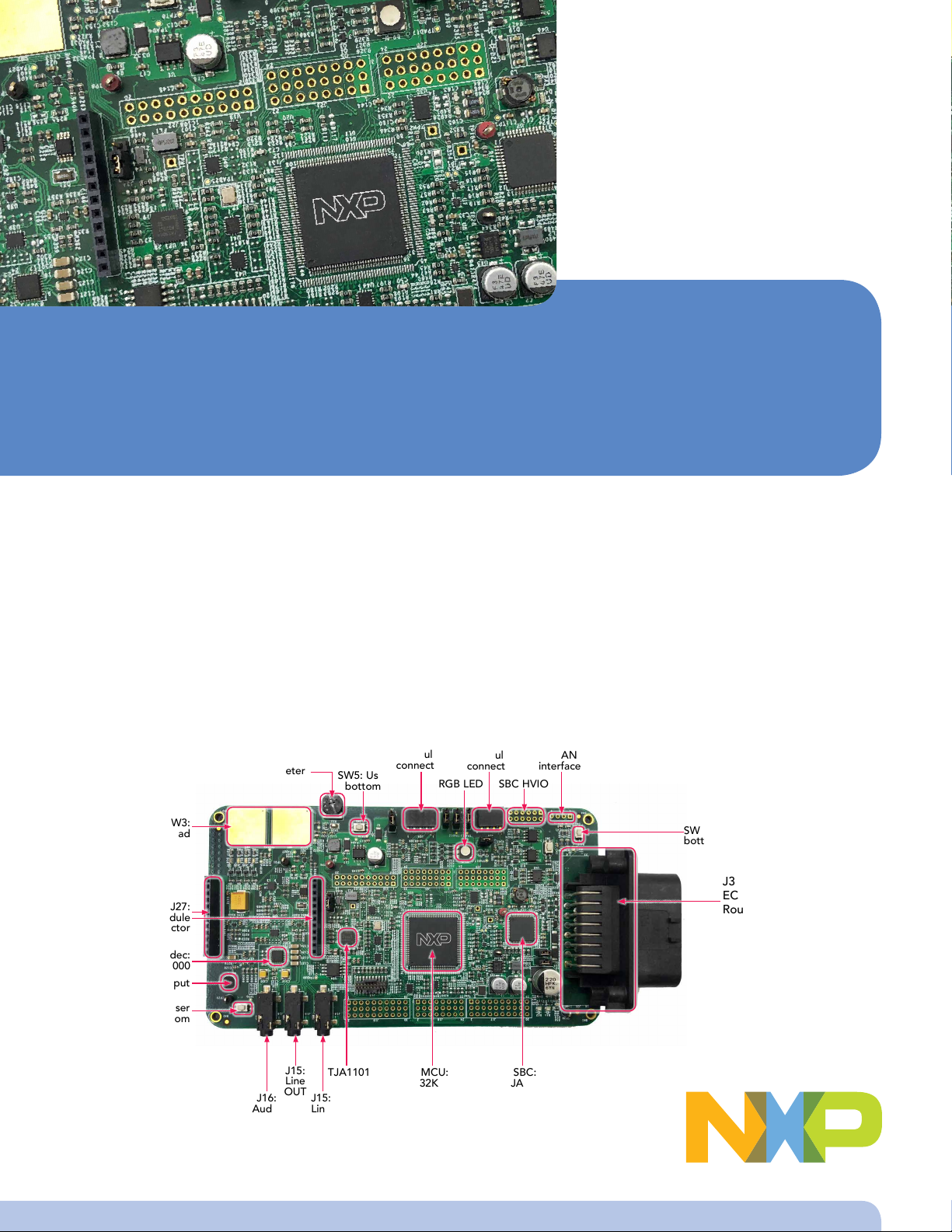
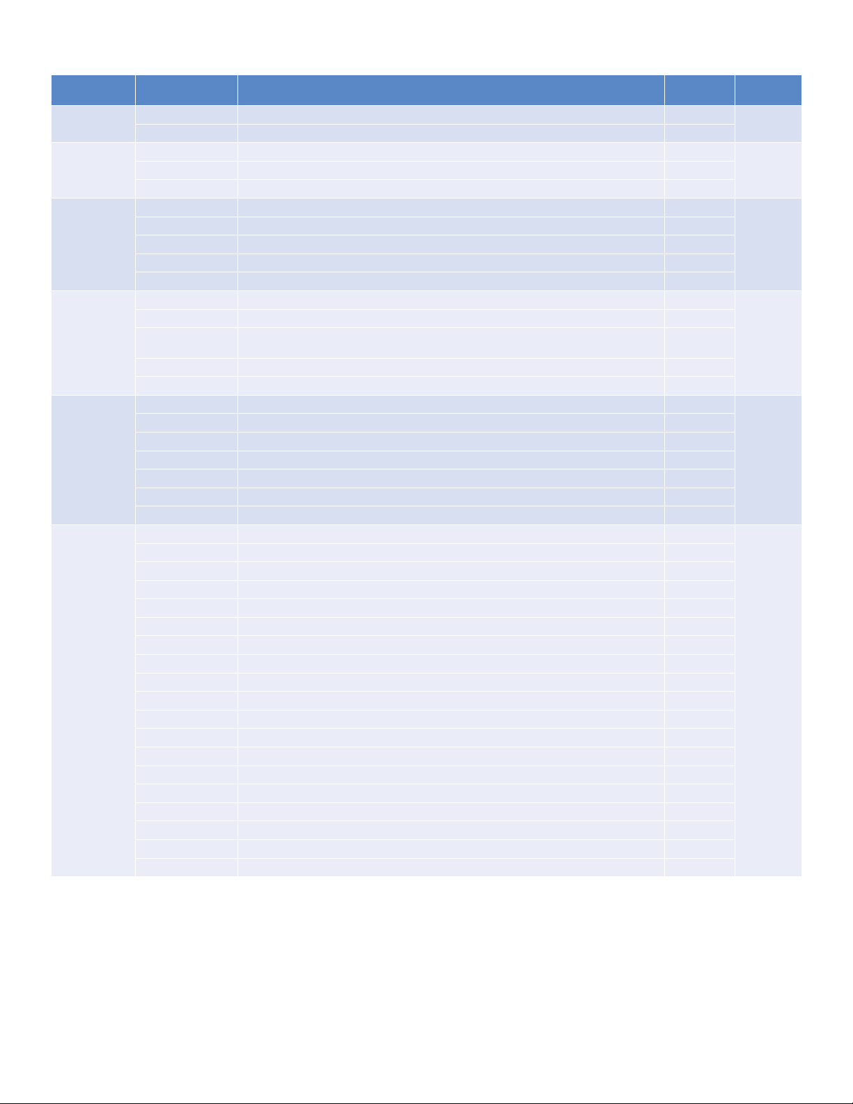
GET TO KNOW THE S32K148-T-BOX REFERENCE DESIGN BOARD (RBD)
Potentiometer
SW5: User
bottom
J28: GPS
module
connector
J26: BLE
module
connector
RGB LED SBC HVIO
J5: CAN0
interface
SW2 & SW3:
Touch Pad
J25&J27:
4G module
connector
Audio Codec:
STGL5000
P1:Mic input
SW4: User
bottom
J16:
Audio
OUT
J15:
TJA1101 MCU:
Line
OUT
J15:
Line
OUT
Figure 1: S32K148-T-BOX Reference Design Board (RBD)
S32K148
SBC:
UJA113x
SW1: Reset
bottom
J31:23-pin
ECU connector
Route signals with:
• 3x CAN bus
• 2x LIN bus
• 1x Ethernet
• 2x Analog input
• 2x HS output
• 2x Input Capture
• 12 V Power Supply
Page 2
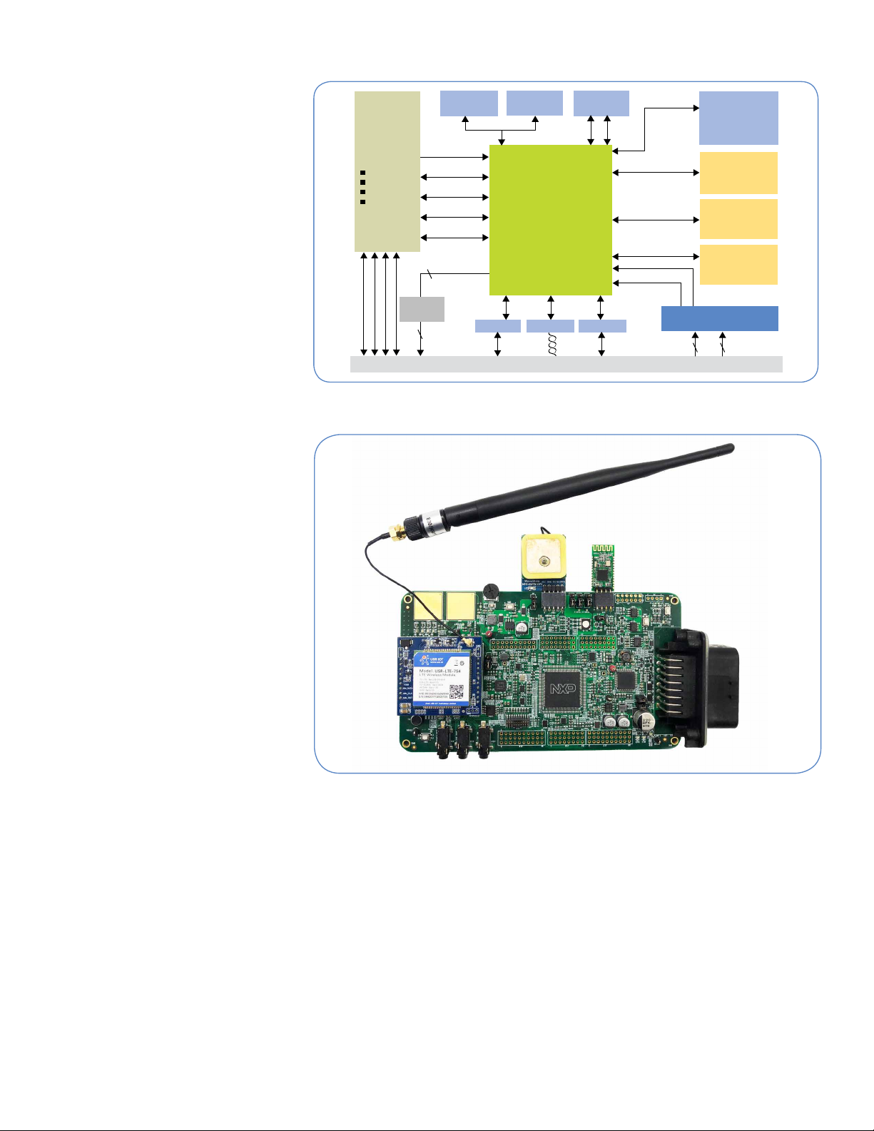
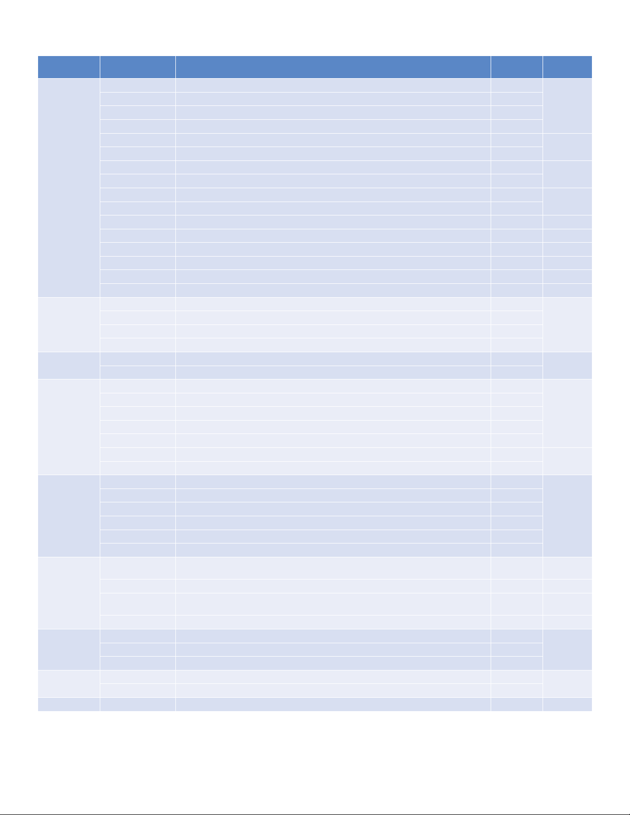
S32K148-T-BOX RDB BLOCK
GPS Module
MCU
S32K148
LQFP-144/176
3G/4G
Communication
Module
UART
I
2
C
8 MB QSPI Flash
External Memory
QSPI
TJA1101
ENET MIICAN/CAN-FD
Standalone
RTC Chip
I
2
C
VBAT/IGN +12 V
SBC
UJA1132
2x 5 V LDO
1x CAN PHY
2 x LIN PHY
8 x HVIO
3-axi
Accelerator
TJA1044
TJA1043
CAN/CAN-FD
SPI
UART
CAN
LIN
LIN
I
2
S
Audio Codec
SGTL5000
UART
BLE Module
2x PWM
5 V @ 500 mA
23-pin ECU connector
HS Driver
2x HS
Signal Conditional Circuit
2x Analog Input 2x PWM Input
2x ADC
2x Input Capture
DIAGRAM
To achieve the maximum flexibility to be
T-BOX/GP-ECU Ref-Design/S32K148 EVB:
BLE, GPS and 3G/4G select
independent Module and connect with
S32K148 via UART
Add QSPI Nor-Flash, standalone
RTC and 3-aix Accelerator for T-Box
functions
Extend a 100M-base TX1 automotive
ethernet via TJA1101 for both T-Box
connection and AVB evaluation (plus a
I2S audio Codec )
SBC provides 5/3.3V power supply for
S32K148 and other onboard modules
and also expends 1 CAN and 2 LIN bus
Select TJA1044 with SO-8 and TJA1043
with HVSON14 package to compatible
with Stinger
S32K148-T-BOX RDB BLOCK DIAGRAM
S32K148 T-BOX_GP-ECU RDB WITH ALL MODULES PLUGIN
Use a 23-pin ECU connector to route
all CAN/LIN/ENET bus and extend 2x
HS output, 2x PWM input capture and
2x Analog Input, enable it to work as a
GP-ECU
S32K148-T-BOX RDB FEATURES
Support S32K148 with LQFP-144
or LQFP-176 pin package(default
mounted with LQFP-144 package)
SBC UJA1132 with 2 LIN physical
layers and 1 CAN physical layer
Integrate communication interfaces:
– 3x CAN with CAN-FD
– 3x UART(2 reused as LIN via SBC-
UJA113x)
– 1x 100M-base TX1 automotive
ethernet via TJA1101
– 1x I2S audio codec extend with
SGTL500 and support AVB
evaluation
Integrate 8MB QSPI NOR Flash
memory(MX25L6433F)
Provide T-BOX function module plugin
interfaces:
1 UART BLE module
1 UART GPS module
1 UART 4G communication module
2x user bottoms input
2x touch sensor input
1x RGB LED
1x Potentiometer
1x 3-axi accelerator(MMA8452Q) via
I2C
1x stand-alone RTC chip(PCA85063)
A 23-pin ECU connector, routing external
I/O signals including:
– 2x ADC input channels
– 2x HS PWM output channels
– 2x PWM input capture channels
– 3x CAN bus
– 2x LIN bus
– 1x 100M-base TX1 automotive
ethernet
Compatible with S32K148EVB:
– Arduino™UNO footprint-compatible
with expansion “shield” support
– Can run all demo projects of SDK
Voltage supply options for 3.3V or 5V
2
Page 3
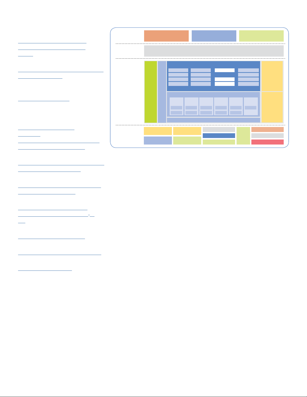
DOCUMENTATION FOR MAIN CHIPS
Application
Software
BSP Layer
T_BOX APP
GPS
Module
BLE
Module
4G Wireless
COM Module
8 MB
QSPI
Flash
Audio
Codec
Standalone RTC
S32K148 MCU
3-axi accelerator
1x ENET interface
2x LIN interface
3x CAN interface
GP_ECU APP BSP_TestPrj
BSP API
S32K SDK
Hardware
S32K148-T-BOX
Reference Design
Board
Processor
Expert UI
Config files
Start-up/
Compiler
linker files
USB
SDHC
ZipWire
FR
Comms Safety
Motor Control
Misc.
Analog
LIN
NFC
CAN
TCP/IP
AMMCLib
sCST
sPTLib
Audio
Touch Sensing
Security
AVB
Comms Safety &
Security
Timers External SoC &
Boards
Middleware
Low-level Drivers
Headers
OS
OSIF
PAL
PD
PAL
PD
PAL
PD
PAL
PD
PAL
PD
PD
AND MODULES
Main MCU: S32K148z
S32K1xx MCU Family Data Sheet(REV 9)
S32K1xx MCU Family Reference
Manual(REV 9)
SBC: UJA1132
UJA113x_SER, Buck/boost HS-CAN/dual
LIN system basis chip(REV 2.2)
100M-base TX1 automotive Ethernet
Transceiver: TJA1101
TJA1101 Full Data Sheet (NDA
Required)(REV 1.0)
CAN Transceiver: TJA1043 and
TJA1044
TJA1043,High-speed CAN
transceiver(REV 6.1)
TJA1044, High-speed CAN transceiver
with Standby mode - Data sheet(REV 6)
S32K148 T-BOX_GP-ECU RDB SW ARCHITECTURE
Audio Codec: SGTL5000
SGTL5000, Low Power Stereo Codec with
Headphone Amp - Data Sheet(REV 6.0)
3-axi Accelerator: MMA8452Q
MMA8452Q, 3-Axis, 12-bit/8-bit Digital
Accelerometer - Data Sheet(REV 10)
Standalone RTC Chip: PCA85063
Automotive tiny Real-Time Clock/
calendar with alarm function and I2Cbus(REV 4.0)
GPS Module
NEO-6M/7M UART GPS module
3G/4G Communication Module
USR-LTE-7S4 UART 4G LTE DTU module
BLE Bluetooth 4.0 Module
HC-08, UART BLE module
* The links are also the purchase link for these modules
S32K148-T-BOX RBD SOFTWARE PACKAGE
The S32K148 T-BOX_GP-ECU RDB SW
package is based on S32K SDK and
is developed to accelerate customer’s
application prototype verification code
development
With the BSP layer, the SW package
provides a set of easy-use API for
application layer use
The SW package includes:
– S32K148 T-BOX_GP-ECU RDB SDK
processor expert configuration
– The GPS/BLE/4G communication/
audio Codec modules driver API and
test codes
– CAN/LIN/UART/I2C communication
driver API and test codes
– FreeRTOS and LwIP based ENET
TCP/IP stack and demo project
– The BSP test project
– The T-BOX reference design demo
project
– Detailed user manual
3
Page 4
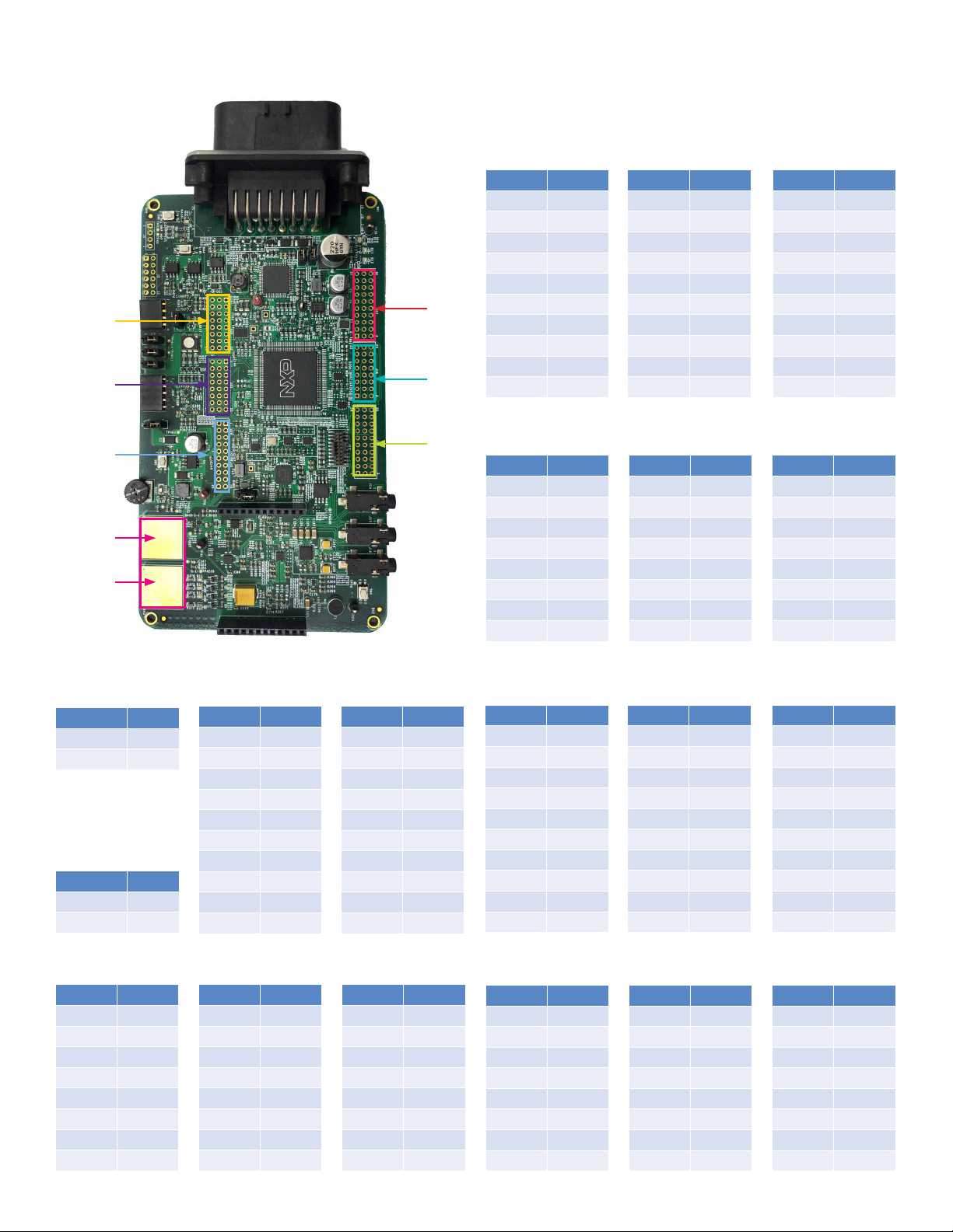
PINOUT MAPPING OF ARDUINO™UNO HEADER
J17
J20
J21
J22
Electrode
A (SW2)
Electrode
B (SW3)
J17
J18
J19
PIN PORT
J17-28 PTE15
J17-25 PTE16
J17-22 VREFH
J17-19 GDN
J17-16 PTB2
J17-13 PTB3
J17-10 PTB1
J17-7 PTB0
J17-4 PTA30
J17-1 PTA31
J18
PIN PORT
J18-22 PTD14
J18-19 PTD15
J18-16 PTD16
J18-13 PTD17
J18-10 PTC10
J18-7 PTC11
J18-4 PTA3
J18-1 PTA2
PIN PORT
J17-29 PTB12
J17-26 PTB13
J17-23 PTE11
J17-20 PTE10
J17-17 PTB11
J17-14 PTB17
J17-11 PTB18
J17-8 PTA6
J17-5 PTA7
J17-2 PTA25
PIN PORT
J18-23 PTA13
J18-20 PTA14
J18-17 PTE2
J18-14 PTE3
J18-11 PTE6
J18-8 PTB7
J18-5 PTE8
J18-2 PTE9
PIN PORT
J17-30 PTD31
J17-27 PTD26
J17-24 PTD25
J17-21 PTC26
J17-18 PTC25
J17-15 PTC24
J17-12 PTC22
J17-9 PTC21
J17-6 PTC20
J17-3 PTC18
PIN PORT
J18-24 PTD20
J18-21 PTD21
J18-18 PTB24
J18-15 PTB26
J18-12 GND
J18-9 GND
J18-6 PTB30
J18-3 PTB31
ELECTRODE A
(SW2)
PIN PORT
TOUCH0_0 PTA0
TOUCH0_1 PTA15
ELECTRODE B
(SW3)
PIN PORT
TOUCH1_0 PTA1
TOUCH1_1 PTA16
J21
PIN PORT
J21-3 PTB17
J21-6 PTA27
J21-9 PTA28
J21-12 PTA29
J21-15 PTA0
J21-18 PTA1
J21-21 PTA15
J21-24 PTA16
J22
PIN PORT
J22-2 PTC15
J22-4 PTB8
J22-6 PTA11
J22-8 PTA12
J22-10 VDD
J22-12 GND
J22-14 PTE1
J22-16 PTE0
J22-18 PTD1
J22-20 PTD13
PIN PORT
J21-2 PTD4
J21-5 PTD22
J21-8 PTD23
J21-11 PTD24
J21-14 PTD27
J21-17 PTD28
J21-20 PTD29
J21-23 PTD30
PIN PORT
J22-1 PTE21
J22-3 PTE22
J22-5 PTE23
J22-7 PTE24
J22-9 PTE25
J22-11 PTC19
J22-13 PTC14
J22-15 PTB14
J22-17 PTB15
J22-19 PTB16
PIN PORT
J21-1 PTC23
J21-4 PTC27
J21-7 PTC28
J21-10 PTC29
J21-13 PTC30
J21-16 PTC31
J21-19 PTE19
J21-22 PTE20
J19
PIN PORT
J19-28 PTD3
J19-25 PTD2
J19-22 PTD19
J19-19 PTD18
J19-16 PTA18
J19-13 PTA19
J19-10 PTB9
J19-7 PTB10
J19-4 PTB21
J19-1 PTB20
J20
PIN PORT
J20-3 VBAT
J20-6 VBAT
J20-9 LIN1
J20-12 GND
J20-15 LIN2
J20-18 GND
J20-21 CANH
J20-24 CANL
PIN PORT
J19-29 PTD0
J19-26 PTE14
J19-23 PTE13
J19-20 PTE12
J19-17 GND
J19-14 VDD
J19-11 PTC6
J19-8 PTC7
J19-5 PTC12
J19-2 PTC13
PIN PORT
J20-2 PTB23
J20-5 PTB22
J20-8 PTB29
J20-11 PTB27
J20-14 PTB28
J20-17 PTB25
J20-20 PTA8
J20-23 PTA9
PIN PORT
J19-30 PTE17
J19-27 PTE18
J19-24 PTB19
J19-21 PTE27
J19-18 PTE26
J19-15 PTA20
J19-12 PTA21
J19-9 PTA22
J19-6 PTA23
J19-3 PTA24
PIN PORT
J20-1 VBAT
J20-4 VDD
J20-7 PTA5
J20-10 V3_3
J20-13 V5_0
J20-16 GND
J20-19 GDN
J20-22 VBAT
4
Page 5
HEADER/PINOUT MAPPING FOR S32K148
External
Modules
BLE module
GPS module
4G module
TJA1044/
Stinger (SO8)
TJA1043/
Stinger (HVON-
14)
TJA1101
(10/100Mbit/s
Ethernet PHY)
Function Pin S32K148 MCU Pins
UART-TX PTB0/LPUART0_RX J26-1
UART-RX PTB1/LPUART0_TX J26-2
UART-TX PTC8/LPUART1_RX J28-3
PPS PTC10/FTM3_CH4/TRGMUX_IN11 J28-1
UTXD1 PTD17/FTM0_FLT2/LPUART2_RX/FTM5_FLT1 J25-6
URXD1 PTE12/FTM0_FLT3/LPUART2_TX/FTM5_FLT0 J25-7
POWER_KEY_N PTD4/FTM0_FLT3/ADC1_SE6 J25-10
M_RELOAD_N PTD2/FTM3_CH4/LPSPI1_SOUT/FXIO_D4/FXIO_D6/ADC1_SE2 J27-6
M_RESET_N PTD3/FTM3_CH5/LPSPI1_PCS0/FXIO_D5/FXIO_D7/ADC1_SE3 J27-7
TXD PTC7/LPUART1_TX/CAN1_TX/FTM3_CH3 NC
RXD PTC6/LPUART1_RX/CAN1_RX/FTM3_CH2 NC
STB PTC11/FTM3_CH5/FTM4_CH2/TRGMUX_IN10 NC
CANH NC J31-2
CANL NC J31-17
TXD PTB13/FTM0_CH1/FTM3_FLT1/CAN2_TX NC
RXD PTB12/FTM0_CH0/FTM3_FLT2/CAN2_RX NC
EN PTB11/FTM3_CH3/LPI2C0_HREQ NC
STB_N PTB15/FTM0_CH3/LPSPI1_SIN/ADC1_SE14 NC
INH SBC_HVIO3 NC
CANH NC J31-3
CANL NC J31-18
MDC PTB5/ENET_MII_RMII_MDC NC
MDIO PTB4/MII_RMII_MDIO NC
INT_N PTB20/FTM6_CH0/ENET_INT NC
RXDV/CONFIG2 PTC17/MII_RMII_RX_DV NC
RXER/CONFIG3 PTC16/MII_RMII_RX_ER NC
RXC/REF_CLK PTD10/MII_RX_CLK NC
RXD0/PHYAD0 PTC1/MII_RMII_RXD0 NC
RXD1/PHYAD1 PTC0/MII_RMII_RXD1 NC
RXD2/CONFIG0 PTD9/MII_RXD2 NC
RXD3/CONFIG1 PTD8/MII_RXD3 NC
TXER PTC3/MII_TX_ER NC
TXEN PTD12/MII_RMII_TX_EN NC
TXD0 PTC2/MII_RMII_TXD0 NC
TXD1 PTD7/MII_RMII_TXD1 NC
TXD2 PTD6/MII_TXD2 NC
TXD3 PTD5/MII_TXD3 NC
INH SBC_HVIO4 NC
TRX_P NC J31-5
TRX_N NC J31-20
On-board
Connector
Used MCU
Peripherals
LPUART0
LPUART1UART-RX PTC9/LPUART1_TX J28-2
LPUART2
CAN1
CAN2
ENET
5
Page 6
HEADER/PINOUT MAPPING FOR S32K148 CONT.
External
Modules
SBC(UJA113X)
External RTC &
ACCELERATOR
Internal RTC
SAI(I2S) AUDIOSGTL5000
QSPIFLASH(64Bit)
Touch PAD
RGB LED
user BUTTOM
Potentiometer ADC test input PTC28/FTM4_CH7/ADC0_SE28 NC ADC0_SE28
Function Pin S32K148 MCU Pins
SBC_SPI_CS PTA26/FTM5_CH1/LPSPI1_PCS0 NC
SBC_SPI_SCLK PTA28/FTM5_CH3/LPSPI1_SCK/LPUART0_RX NC
SBC_SPI_MOSI PTA29/FTM5_CH4/LPUART2_TX/LPSPI1_SIN NC
SBC_SPI_MISO PTA27/FTM5_CH2/LPSPI1_SOUT/LPUART0_TX NC
SBC_CAN_TXD PTE5/TCLK2/FTM2_CH3/CAN0_TX/FXIO_D7 NC
SBC_CAN_RXD PTE4/TRACE_D1/FTM2_CH2/CAN0_RX/FXIO_D6 NC
SBC_LIN1_TXD PTA3/LPUART0_TX/FXIO_D5 NC
SBC_LIN1_RXD PTA2/LPUART0_RX/FXIO_D4 NC
SBC_LIN2_TXD PTA9/LPUART2_TX/LPSPI2_PCS0/FXIO_D7/FTM3_FLT2 NC
SBC_LIN2_RXD PTA8/LPUART2_RX/LPSPI2_SOUT/FXIO_D6/FTM3_FLT3 NC
SBC_CANH NC J5-1
SBC_CANL NC J5-2
SBC_LIN1 NC J31-10
SBC_LIN2 NC J31-11
INTN1 PTE19/FTM7_CH7/FTM7_CH7/ADC1_SE25 NC
INTN2 PTE20/FTM4_CH0/FTM4_CH0/ADC1_SE26 NC
I2C_SCL PTD19/FTM6_CH0/FXIO_D3/LPI2C1_SCL/ADC1_SE17 NC
I2C_SDA PTC31/FTM5_CH6/FXIO_D1/LPI2C1_SDA/FXIO_D1/ADC0_SE31 NC
ACC_INT1 PTD22/FTM6_CH3/FTM6_CH3/ADC1_SE18 NC
ACC_INT2/RTC_INT PTD23/FTM6_CH4/FTM6_CH4/ADC1_SE19 NC
RTC_CLKIN PTA7/FTM0_FLT2/FTM5_CH3/RTC_CLKIN/LPUART1_RTS/ADC0_SE3 NC
RTC_CLK_EN PTA6/FTM0_FLT1/LPSPI1_PCS1/FTM5_CH5/LPUART1_CTS/ADC0_SE2 NC
SYS_MCLK PTD1/FTM0_CH3/LPSPI1_SIN/FTM2_CH1/SAI0_MCLK NC
I2S_SCLK PTA12/FTM1_CH6/CAN1_RX/LPI2C1_SDAS/SAI0_BCLK NC
I2S_LRCLK PTA11/FTM1_CH5/FXIO_D1/CMP0_RRT/SAI0_SYNC NC
I2S_DIN PTA13/FTM1_CH7/FTM2_QD_PHA/SAI0_D0 NC
I2S_DOUT PTE1/LPSPI0_SIN/LPI2C0_HREQ/LPI2C1_SCL/SAI0_D1 NC
CTRL_CLK PTA3/LPUART0_TX/LPI2C0_SCL/FXIO_D5 NC
CTRL_DATA PTA2/LPUART0_RXLPI2C0_SDA//FXIO_D4 NC
SCLK PTD10/QSPI_A_SCK NC
CS_N PTC3/QSPI_A_CS NC
SI/SIO0 PTD11/QSPI_A_IO0 NC
SO/SIO1 PTD7/QSPI_A_IO1 NC
WP_N/SIO2 PTD12/QSPI_A_IO2 NC
HOLD_N/SIO3 PTC2/QSPI_A_IO3 NC
TOUCH_ADC0_A
TOUCH_ADC1_A PTA15/FTM1_CH2/LPSPI0_PCS3/LPSPI2_PCS3/FTM7_FLT0/ADC1_SE12 NC ADC1_SE12
TOUCH_ADC0_B
TOUCH_ADC1_B PTA16/FTM1_CH3/LPSPI1_PCS2/ADC1_SE13 NC ADC1_SE13
LED_RED PTE21/FTM4_CH1/ADC1_SE27 NC
LED_GREEN PTE22/FTM4_CH2/ADC1_SE28 NC
LED_BLUE PTE23/FTM4_CH3/ADC1_SE29 NC
BTN0 PTC12/FTM3_CH6/FTM2_CH6/LPUART2_CTS NC
BTN1 PTC13/FTM3_CH7/FTM2_CH7/LPUART2_RTS NC
PTA0/FTM2_CH1/LPI2C0_SCLS/FXIO_D2/FTM2_QD_PHA/LPUART0_CTS/TRGMUX_OUT3/
ADC0_SE0/CMP0_IN
PTA1/FTM1_CH1/LPI2C0_SDAS/FXIO_D3/FTM1_QD_PHA/LPUART0_RTS/TRGMUX_OUT0/
ADC0_SE1/CMP0_IN1
On-board
Connector
NC ADC0_SE0
NC ADC0_SE1
Used MCU
Peripherals
PTE work as
PTC work as
input/EIRQ
LPSPI1
CAN0
LPUART0/
FlexIO4_5
LPUART2/
FlexIO6_7
LPI2C1
RTC
SAI0
LPI2C0/
FLEXIO
QSPI_A
output
6
Page 7
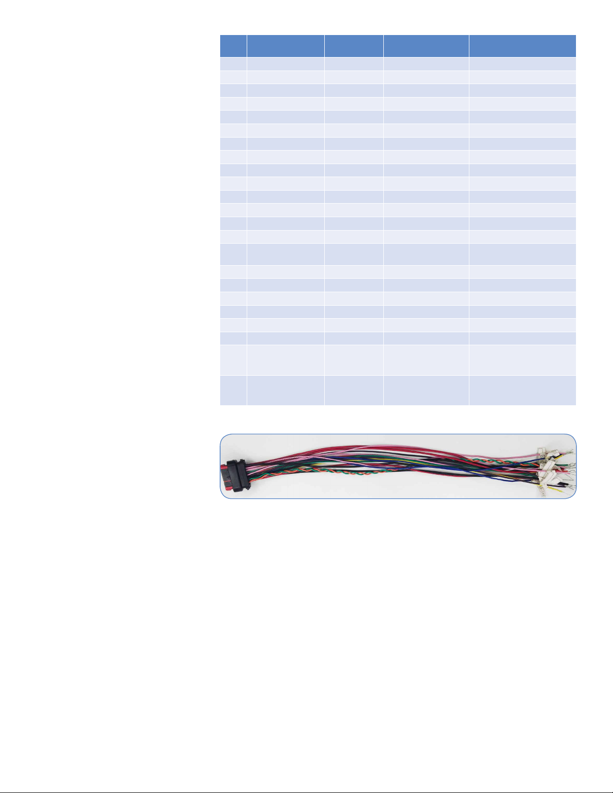
23-PIN ECU CONNECTOR SIGNAL
ROUTING AND WIRING HARNESS
The 23-pin ECU connector, routing
communication and external I/O
signals including:
– 2x ADC input channels;
– 2x HS PWM output channels;
– 2x PWM input capture channels;
– 3x CAN bus;
– 2x LIN bus;
– 1x 100M-base TX1 automotive
ethernet;
– +12V VBAT power supply input;
– +5V power supply output for
external devices;
The 23-pin ECU connector enables the
board to work as GP-ECU easily:
The 23-pin ECU connector matched
wiring harness with signal labels as
below photo.
It is not included in S32K148 T-BOX
RDB, please contact NXP sales for
purchase:
PIN# Signal Wire color
1 VBAT red 1.25 12V @ max 5A
2 CAN1H yellow 0.5 CAN bus 1 differential signal+
3 CAN2H yellow 0.5 CAN bus 2 differential signal+
4 ECU_EXT_HS1 green 0.5 ECU High Side driver output 1
5 CAN0H yellow 0.5 CAN bus 0 differential signal+
6 ECU_EXT_ADC1 blue 0.5 ECU external analog input 1
7 ECU_EXT_ADC2 blue 0.5 ECU external analog input 2
8 GND black 1.25 Power/signal ground
9 VBAT red 1.25 12V @ max 5A
10 ECU_EXT_LIN1 white 0.5 LIN bus 1
11 ECU_EXT_LIN2 white 0.5 LIN bus 2
12 SBC_HVIO5 orange 0.5 SBC HVIO5
13 ECU_EXT_PWM2 purple 0.5 PWM input channel 2
14 ECU_EXT_PWM1 purple 0.5 PWM input channel 1
15 ECU_EXT_5V red 0.75
16 GND black 1.25 Power/signal ground
17 CANL1 pink 0.5 CAN bus 1 differential signal-
18 CANL2 pink 0.5 CAN bus 2 differential signal-
19 ECU_EXT_HS2 green 0.5 ECU High Side driver output 2
20 CANL0 pink 0.5 CAN bus 0 differential signal-
21 GND black 1.25 Signal ground
22 ENET_TRX_P green 0.5
23 ENET_TRX_N orange 0.5
Wire gauge
(conductor CSA/mm2)
description
5V power supply for ECU
external device@max100mA
100M-base TX1 automotive
ethernet differential signal+,
UTP
100M-base TX1 automotive
ethernet differential signal -,
UTP
7
Page 8
JUMPER SETTINGS (POWER SUPPLY)
Jumper Configuration Description
J2
J8
J9
J29
J11 1-2 (Default)
The jumper connection schematic is as below, details can be found in the board schematic;
1-2 (Default) The 3.3V supply powered from VBAT(+12V);
2-3 The 3.3V supply powered from P5V0(5V);
1-2 (Default) The P5V0 supply powered from SBC output ;
2-3 Not use, no power source(NC on J8-3);
1-2 (Default) The VDD supply powered from P3V3_SW(3.3V);
2-3 The VDD supply powered from P5V0(5V);
1-2 (Default) VCAN_SBC supply powered from P5V0_V1SBC;
2-3 VCAN_SBC supply powered from PVEXT_SBC;
It’s connected between VDD and VDD_MCU, and is designed for
S32K148 MCU low-power static current measurement, for this case,
R77 needs to be unmounted.
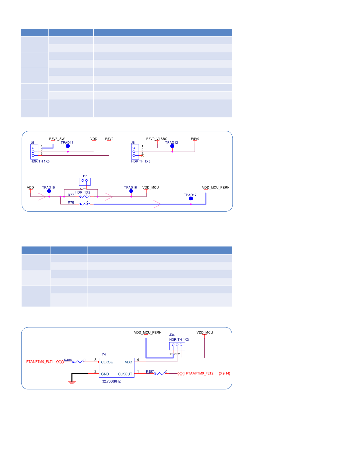
JUMPER SETTINGS (LIN AND RTC CLOCK CONFIGURATION)
Jumper Configuration Description
J32
J33
J34
External active 32.768 KHz oscillator for RTC schematic is as right, details can be found in the board
schematic and HW UG;
short (Default) Enable the LIN bus 1 pullup to work as a master node;
open The LIN bus 1 is working as a slave node;
short (Default) Enable the LIN bus 2 pullup to work as a master node;
open The LIN bus 2 is working as a slave node;
1-2 (Default) External active 32.768KHz oscillator for RTC is powered by VDD_MCU;
2-3
External active 32.768KHz oscillator for RTC is powered by VDD_MCU_
PERH;
8
Page 9

USING ETHERNET AND QSPI
IMPORTANT OBSERVATION
The S32K148 is the only member of the
family able to use ethernet and QuadSPI.
However, these interfaces are mutually
exclusive so only one of them can be
used at a time. In order to use either
Ethernet or QuadSPI, user must follow
an specific resistor configuration. The
default configuration of the board is to
be used for ethernet communication.
CHANGE 0Ω CONFIGURATION
RESISTORS TO REUSE BETWEEN
ENET AND QUADSPI
For S32K148 T-BOX RDB, some ENET
and QuadSPI data lines are shared
from the MCU, each interface is
separated by two 0 Ω resistors
By default the ENET data lines are
enabled
User can change the 0Ω configuration
resistors to enable and use QuadSPI:
S32K148 shared PIN Configuration resistor Description
PTD7 R161 (Default) ENET: MII_RMII_TXD1
R162 QuadSPI: QSPI_A_IO1
PTC2 R177(Default) ENET: MII_RMII_TXD0
R178 QuadSPI: QSPI_A_IO3
PTC3 R196 (Default) ENET: MII_TX_ER
R203 QuadSPI: QSPI_A_CS
PTD10 R178 (Default) ENET: MII_RX_CLK
R179 QuadSPI: QSPI_A_SCK
PTD11 R194 (Default) ENET: MII_RMII_TX_CLK
R195 QuadSPI: QSPI_A_IO0
PTD12 R190 (Default) ENET: MII_RMII_TX_EN
R192 QuadSPI: QSPI_A_IO2
9
Page 10

S32K148-T-BOX RDB
USB Cable to PC
DC - 12 V
power supply
Out-of-the-Box Setup
POWER UP THE BOARD AND
DEBUGGER CONNECTION
The S32K148 T-BOX RDB powers from
external +12V power supply via the
23-pin ECU connector with the wiring
harness. If no 23-pin ECU connector
wiring harness available, the board be
powered by J31-8 (GND) and J31-1
(+12V)
Note: There is no embedded debugger
(e.g. OpenSDA) on the RDB, so debug
is done using PEMicro U-Multilink/FX
through J12 with a mini-20 pin cable on
debugger’s port F
After power on, the D10, D11 and D12
on the left up corner of the board will
light on
With Connecting the U-Multilink
debugger to PC, its USB and TGTPWR
LED will be lighted on
S32K148 T-BOX RDB SETUP CONNECTION
10
Page 11

Use the BSP test project
STEP 1: DOWNLOAD & INSTALL S32DS FOR ARM V2018.R1 AND S32K SDK RTM 2.0.0
Download S32DS for ARM v2018.R1 from the following link:
http://www.nxp.com/S32DS
– The download will require a NXP account login, user can register the account with any e-mail, and after download, you can
install S32DS IDE with a 32-bit active code received by the e-mail when download
Download and install the S32K SDK RTM 2.0.0
– S32 Design Studio for Arm® 2018.R1 Update 6 SDK S32K14x RTM v.2.0.0(REV UP6)
Any questions, please refer to the following NXP technical community for help:
https://community.nxp.com/docs/DOC-335302
STEP 2: IMPORT AND COMPILE THE BSP TEST PROJECT (1)
Open S32DS for ARM v2018.R1 IDE select File > Import.
Select General > Existing Projects into Workspace > Next
11
Page 12

STEP 2: IMPORT AND COMPILE THE BSP TEST PROJECT (2)
Select archive file > Browse, browse and choose S32K148_Based_T_BOX_BSP_TestPrj_SDK_RTM2_0.zip, select the project >
Finish:
After importing the project, clean it at first: select the project in Project Explorer, then right-click, choose Clean Project:
12
Page 13

STEP 2: IMPORT AND COMPILE THE BSP TEST PROJECT (3)
Select the project in Project Explorer, then right-click, choose Build Project:
The compile result is as below if no errors are found:
13
Page 14

STEP 3: DOWNLOAD AND DEBUG THE BSP TEST PROJECT
Select the project in Project Explorer, then right-click, choose Debug As > Debug Configuration:
In the Debug Configuration window, select the GDB PEMicro Interface Debugging > S32K148_Based_T_BOX_BSP_TestPrj_
SDK_RTM2_0_Debug>Debugger>under Interface select right debugger, and ensure Port has the right part number, then in
Additional Options, check Emergency Kinetis Device Recovery by Full Chip Erase and Use SWD protocol (if not check this
option, it will use JTAG debug protocol), at last, click Debug to launch the debug(it will download the compile result—elf file in
to the target MCU at first):
14
Page 15

STEP 4: CONNECT THE UART CONSOLE FOR TEST RESULT OUTPUT DISPLAY
The BSP test project use S32K148 LPUART2 to output the test result;
Use a USB-to-UART adapter to connect the board with PC via J25-6(TXD), J25-7(RXD) and J25-12(GND):
* For more details on the test results description and demo projects, please refer to the Software User Guide.
Open a UART console(e.g. Serial Port Utility) on PC, configure its serial communication format as the following:
– Data rate: 115200 baud/s;
– Data Bits: 8;
– Parity: None;
– Stop Bits: 1
– Flow Control: OFF
Then you can see the test result output as below:
15
Page 16

RDB Software package overview
OTHER DEMO PROJECTS
Besides of the BSP test project, which includes the SDK API based LLD of GPS module, BLE module, MMA8452Q,
PCA85063ATT, 3x FlexCAN, 3x LPUART communication, 2x HS(PWM), 2x user bottom, GPIO IRQ interrupt, RGB LED, 2x
input capture, 2x external analog input, 2x Touch Sense PAD and etc.
The SW package also provides the following demo projects:
– QSPI Flash test project
– LwIP based ENET and TJA1101 TCP/IP sever/client communication demo project
– LIN stack based Single board LIN master and slave communication demo project
– I2S audio codec—SGTL500 demo project
– T-BOX reference design project
* For more details, please refer to the S32K148 T-BOX_GP-ECU RDB SW user guide and download the SW package
16
Page 17

Create a New Project in
S32 Design Studio
CREATE NEW PROJECT: FIRST TIME – SELECT A WORKSPACE
Start program: Click on “S32 Design Studio for ARM v1.0” icon
Select workspace:
– Choose default (see below example) or specify new one
– Suggestion: Uncheck the box “Use this as the default and do not ask again”
– Click OK
CREATE NEW PROJECT: TOP MENU SELECTION
File – New –Project
17
Page 18

CREATE NEW PROJECT: S32DS PROJECT
Project Name:
– Example: FirstProject
Project Type:
– Select from inside executable or library folder
Next
Select Debugger Support and Library Support
Click Finish
18
Page 19

OPENSDA CONFIGURATION
To Debug your project with OpenSDA, it is necessary to select the OpenSDA in the Debug Configuration.
Select your project, and click on debug configuration
Select the Debug configuration under GDB PEMicro Interface Debugging
Click on Debugger tab
Select OpenSDA as the interface, if your board is plugged should appear in the Port field.
Click Apply and debug to finish.
19
Page 20

Debug Basics
DEBUG BASICS: STARTING THE DEBUGGER
Debug configuration is only required once. Subsequent starting of debugger does not require those steps.
Three options to start debugger:
– If the “Debug Configuration” has not been closed, click on “Debug” button on bottom right
– Select Run – Debug (or hit F11)
Note: This method currently selects the desktop target (project.elf) and gives an error. Do not use until this is changed.
Recommended Method: Click on pull down arrow for bug icon and select …_debug.elf target
DEBUG BASICS: STEP, RUN, SUSPEND, RESUME
Step Into (F5)
Step Over (F6)
Step Return (F7)
Run
Suspend
Resume (F8)
20
Page 21

DEBUG BASICS: VIEW & ALTER VARIABLES
View variables in “Variables” tab.
Click on a value to allow typing in a different value.
DEBUG BASICS: VIEW AND ALTER REGISTERS
View CPU registers in the “Registers” tab
Click on a value to allow typing in a different value
View peripheral registers in the EmbSys Registers tab
DEBUG BASICS: VIEW AND ALTER MEMORY
Add Memory Monitor
Select Base Address to Start at : 40000000
View Memory
21
Page 22

DEBUG BASICS: BREAKPOINTS
Add Breakpoint: Point and Click
Light blue dot represents debugger breakpoint
DEBUG BASICS: RESET & TERMINATE DEBUG SESSION
Reset program counter
Terminate Ctl+F2()
22
Page 23

Create a P&E Debug Configuration
(Optional)
NEW P&E DEBUG CONFIGURATION
Click in debug configurations
Create a new P&E launch configuration
Select S32K144 device
Click Apply and debug your application
23
Page 24

www.nxp.com/S32K148-T-BOX
NXP and the NXP logo are trad emark s of NXP B.V. All other p roduc t or ser vice nam es are the p roper ty of their respecti ve owner s.
© 2019 NXP B.V.
Docum ent Numb er: S32K148TBOXEFS REV 0
 Loading...