

Page 1

AN5426
Hardware Design Guidelines for S32K1xx Microcontrollers
Rev. 3 — December 2018
Contents
1 Introduction
The S32K series further extends the highly scalable portfolio of ARM
Cortex® MCUs in the automotive industry. It builds on the legacy of the KEA
series, whilst introducing higher memory options alongside a richer peripheral
set extending capability into a variety of automotive applications.
With a 2.70–5.5 V supply and focus on automotive environment robustness,
the S32K series devices are well suited to a wide range of applications in
electrical harsh environments. These devices are optimized for cost-sensitive
applications offering low pin-count options.
The S32K series offers a broad range of memory, peripherals, and package
options. They share common peripherals and pin counts allowing developers
to migrate easily within the MCU family or among the MCU families to take
advantage of more memory or feature integration. This scalability allows
developers to standardize on the S32K series for their end product platforms,
maximizing hardware and software reuse and reducing timeto-market.
Following are the general features of the S32K series MCUs:
• 32-bit ARM Cortex-M4 core with IEEE-754 compliant FPU, executing up
to 112 MHz
• Scalable memory footprints up to 2 MB flash and up to 256 KB SRAM
• Precision mixed-signal capability with on chip analog comparators and
multiple 12-bit ADCs
• Powerful timers for a broad range of applications including motor control,
lighting control and body applications
• Serial communication interfaces such as LPUART, LPSPI, LPI2C,
FlexCAN, CAN-FD, FlexIO and so on.
• SHE specification compliant security module
• Single power supply (2.70–5.5 V) with full functional flash program/
erase/read operations
• Functional safety compliance with ISO26262, with internal watchdog,
voltage monitors, clock monitors, memory protection and ECC
®
1 Introduction..........................................1
2 S32K family comparison..................... 1
3 Power supplies.................................... 2
3.1 Bulk and decoupling
capacitors ...............................3
4 Clock circuitry......................................3
4.1 EXTAL and XTAL pins.............3
4.2 Suggestions for the PCB
layout of oscillator circuit......... 4
5 Debug and programing interface....... 5
5.1 Debug connector pinouts........6
5.2 RESET system......................11
6 Analog comparator interface............ 11
7 Communication modules.................. 13
7.1 LIN interface for LPUART
module...................................13
7.2 CAN interface for FlexCAN
module...................................17
7.3 Inter-Integrated Circuit IIC......20
7.4 Ethernet MAC Interface......... 22
8 Quad Serial Peripheral Interface...... 23
9 Unused pins....................................... 26
10 General board layout guidelines.... 27
10.1 Traces recommendations.... 27
10.2 Grounding .......................... 27
10.3 EMI/EMC and ESD
considerations for layout....... 28
11 PCB layer stacking...........................30
12 Injection current...............................31
13 References........................................31
14 Revision history...............................31
Application Note
• Ambient operation temperature range: –40 °C to 125°C
• Software enablement: S32 Software Development Kit (SDK), S32 Design Studio (S32DS)
S32K family comparison
2
Please refer to the latest version of the Reference Manual for details.
Page 2
NXP Semiconductors
3 Power supplies
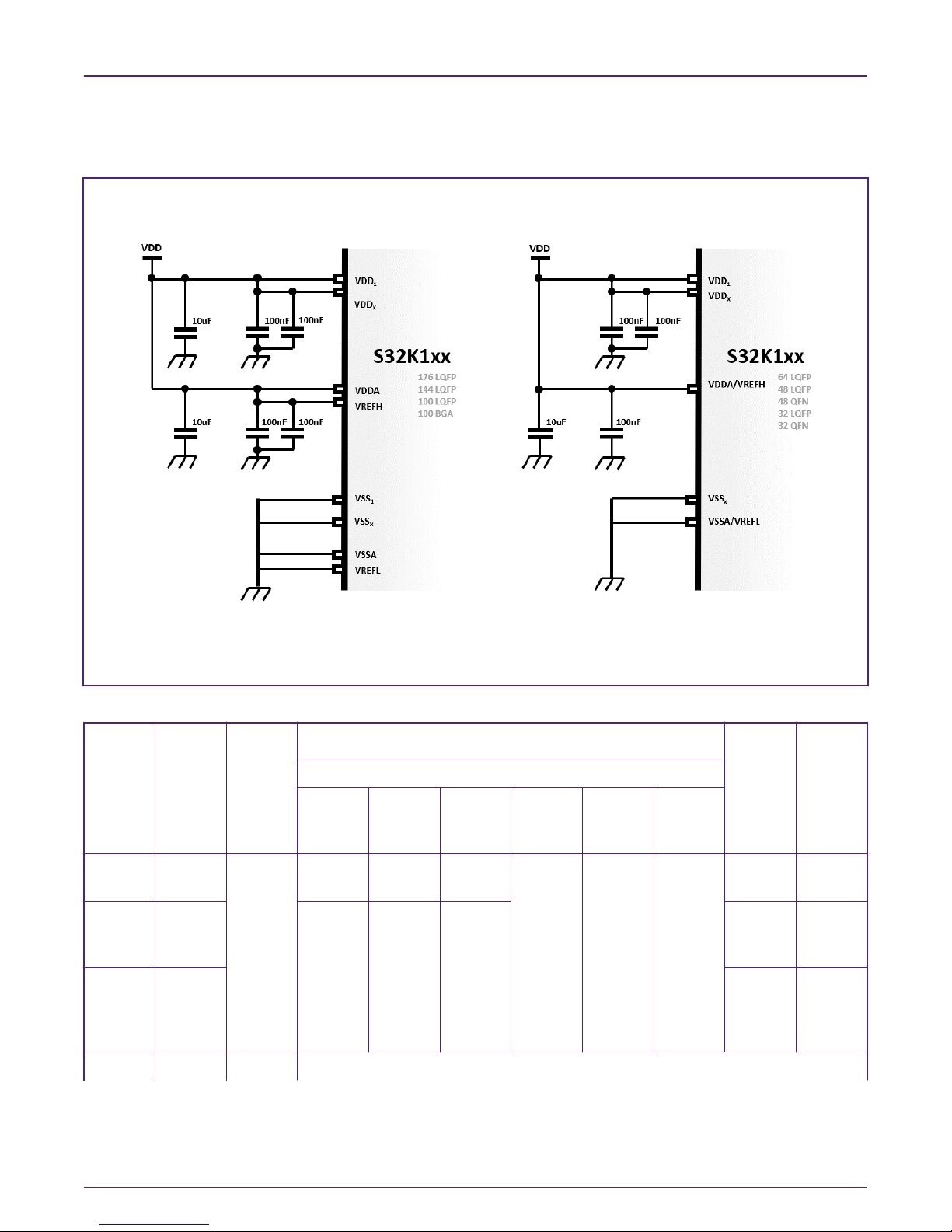
The power and ground pins are described in subsequent sections.
Power supplies
Figure 1. Power supply pins
Table 1. Power domains and decoupling capacitors
Power
DescriptionVoltage
Bulk/Bypass Capacitor for domain Decoupli
Domain
VDDX
176
LQFP
1
Supply
5 V/3.3 V 10uF 10uF 10uF 10uF 10uF 10uF 0.1uF X7R
144
LQFP
voltage
1
VDDA
Analog
10uF 10uF 10uF 0.1uF X7R
supply
voltage
VREFH1ADC
reference
voltage
high
VSS
Ground GND VSS, VSSA and VREFL must be shorted to GND at package level.
Table continues on the next page...
100
LQFP/
BGA
Package
64 LQFP 48 LQFP/
QFN
32 LQFP/
QFN
Characte
ng
ristics
Capacito
r
per pin
Ceramic
Ceramic
0.1uF X7R
Ceramic
Hardware Design Guidelines for S32K1xx Microcontrollers , Rev. 3, December 2018
Application Note
2 / 33
Page 3

NXP Semiconductors
Table 1. Power domains and decoupling capacitors (continued)
Clock circuitry
VSSA
VREFL
1. VDD and VDDA must be shorted to a common reference on PCB. Appropriate decoupling capacitors to be used to filter
noise on the supplies
Analog
Ground
ADC
reference
voltage
low
3.1 Bulk and decoupling capacitors
The bulk capacitor acts as a local power supply to the power pin, near the decoupling capacitors. Minimize the trace length
between the bulk capacitor and the decoupling capacitors.
Decoupling capacitors make the current loop between supply, MCU, and ground reference as short as possible for high frequency
transients and noise. Therefore, all decoupling capacitors should be placed as close as possible to each of their respective power
supply pin; the ground side of the decoupling capacitor should have a via to the pad which goes directly down to the ground plane.
The capacitor should not route to the power plane through a long trace.
4 Clock circuitry
The S32K1xx has the following clock sources:
• Fast internal reference clock (FIRC): 48 MHz.
• Slow internal reference clock (SIRC): 8 MHz.
• PLL: External oscillator as input source.
• External square wave input clock: up to 50 MHz.
• External oscillator clock (OSC): 4–40 MHz.
FIRC, SIRC are internal and does not have to be considered from the hardware design perspective. The external oscillator works
with a range from 4–40 MHz. It provides an output clock that can be provided to the PLL or used as clock source for some
peripherals. When using the external oscillator as input source for the PLL, the frequency range of the external oscillator should
be 8–40 MHz.
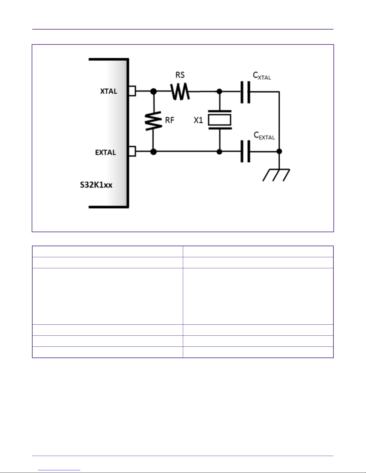
EXTAL and XTAL pins
4.1
These pins provide the interface for a crystal to control the internal clock generator circuitry. EXTAL is the input to the crystal
oscillator amplifier. XTAL is the output of the crystal oscillator amplifier. The pierce oscillator provides a robust, low-noise and lowpower external clock source. It is designed for optimal start-up margin with typical crystal oscillators. S32K1xx supports crystals
or resonators from 4 MHz to 40 MHz. The Input Capacitance of the EXTAL, XTAL pins is 7 pF.
Hardware Design Guidelines for S32K1xx Microcontrollers , Rev. 3, December 2018
Application Note
3 / 33
Page 4
NXP Semiconductors
Clock circuitry
Figure 2. Reference oscillator circuit
Table 2. Components of the oscillator circuit
Symbol Description
RS Bias Resistor
RF
Feedback Resistor
• When Low-gain is selected, internal RF will be selected,
and external RF is not required.
• When High-gain is selected, external RF(1M Ohm) need
to be connected for proper operation of crystal. For
external resistor, up to 5% tolerance is allowed.
X1 Quartz Crystal / Ceramic Resonator
C
C
XTAL
EXTAL
Stabilizing Capacitor
Stabilizing Capacitor
The load capacitors are dependent on the specifications of the crystal and on the board capacitance. It is recommended to have
the crystal manufacturer evaluate the crystal on the PCB.
4.2
Suggestions for the PCB layout of oscillator circuit
The crystal oscillator is an analog circuit and must be designed carefully and according to the analog-board layout rules:
• External feedback resistor [Rf] is not needed because it’s already integrated.
Hardware Design Guidelines for S32K1xx Microcontrollers , Rev. 3, December 2018
Application Note
4 / 33
Page 5
NXP Semiconductors
Debug and programing interface
• It is recommended to send the PCB to the crystal manufacturer to determine the negative oscillation margin as well as the
optimum regarding C
and C
. These values together with the expected PCB, pin, etc. stray capacity values should be used as a starting
EXTAL
XTAL
and C
capacitors. The data sheet includes recommendations for the tank capacitors C
EXTAL
point.
• Signal traces between the XTAL/EXTAL pins, the crystal and the external capacitors must be as short as possible, without
using any via. This minimizes parasitic capacitance and sensitivity to crosstalk and EMI. The capacitance of the signal
traces must be considered when dimensioning the load capacitors.
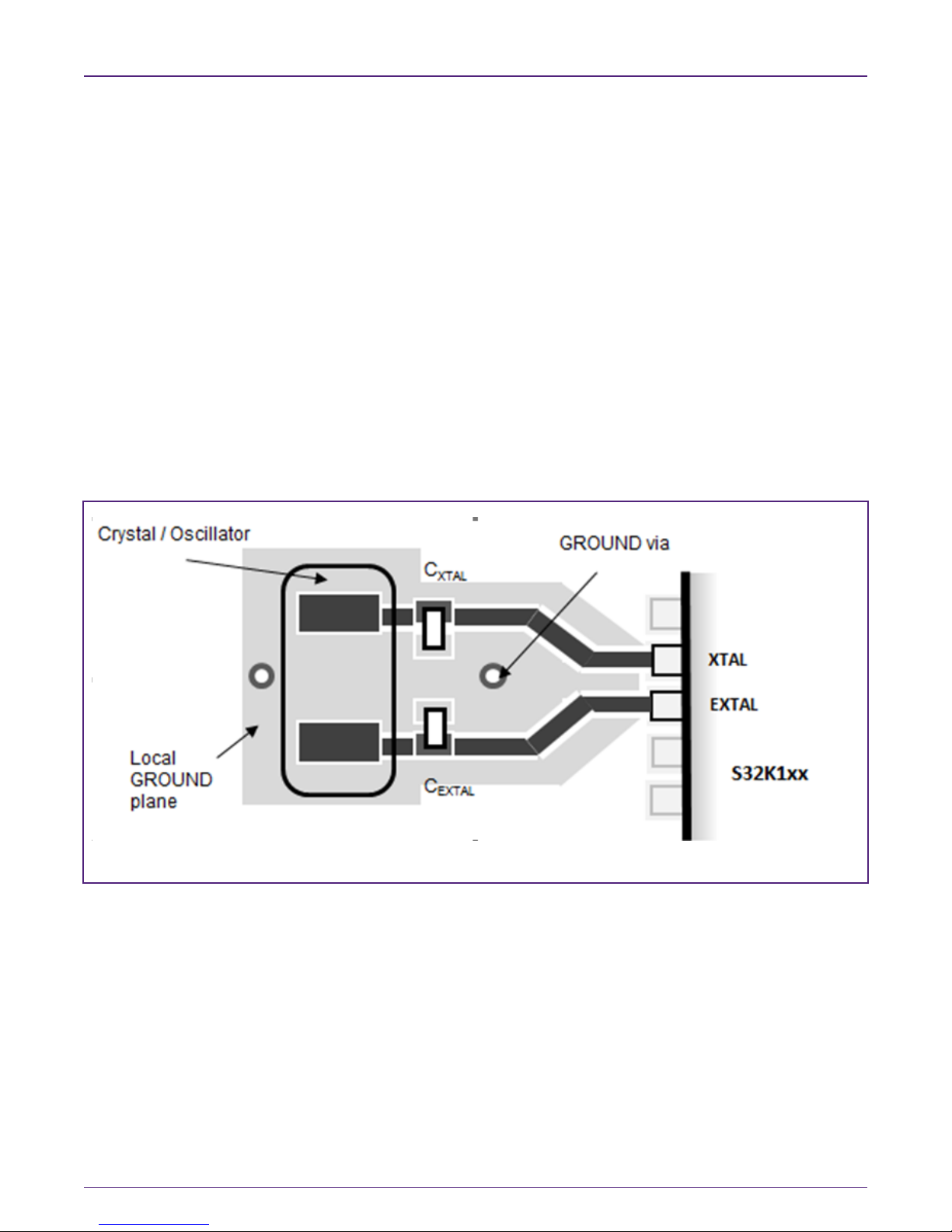
• In case there is only 1-2 PCB layers, it is recommended to place a guard ring around the oscillator components and to
connect it to the a solid ground plane. A ground area should be placed under the crystal oscillator area. This ground guard
ring must be clean ground. This means that no current from and to other devices should be flowing through the guard ring.
This guard ring should be connected to VSS x of the S32K1xx with a short trace. Never connect the ground guard ring to
any other ground signal on the board. Also avoid implementing ground loops.
XTAL
• The main oscillation loop current is flowing between the crystal and the load capacitors. This signal path (crystal to C
to
to crystal) should be kept as short as possible and should have a symmetric layout. Hence, both capacitor’s
CXTAL
ground connections should always be as close together as possible.
• The EXTAL and XTAL pins should only be connected to required oscillator components and must not be connected to any
other devices.
The following figure 3, shows the recommended placement and routing for the oscillator layout.
EXTAL
Figure 3. Suggested crystal oscillator layout
5 Debug and programing interface
A number of commonly used debug connectors are shown here. Most of the ARM development tools uses one of these pin out’s.
When developing your ARM circuit board, it is recommended to use a standard debug signal arrangement to make connection
to debugger easier.
The SWD/SWV pins are overlaid on top of the JTAG pins as follows:
Hardware Design Guidelines for S32K1xx Microcontrollers , Rev. 3, December 2018
Application Note
5 / 33
Page 6
NXP Semiconductors
Debug and programing interface
Table 3. JTAG signal description
JTAG Mode SWD Mode Signal
TCK SWCLK Clock into the core
TDI - JTAG Test Data Input
TDO SWV JTAG Test Data Output / SWV trace data output
(SWO)
TMS SWDIO JTAG Test Mode Select / SWD data in/out
GND GND -
The pull up/down resitors for the JTAG signals are included internally by the default pad configuration. See the device reference
manual and datasheet.
5.1
Debug connector pinouts
5.1.1 20-pin Cortex Debug D ETM connector
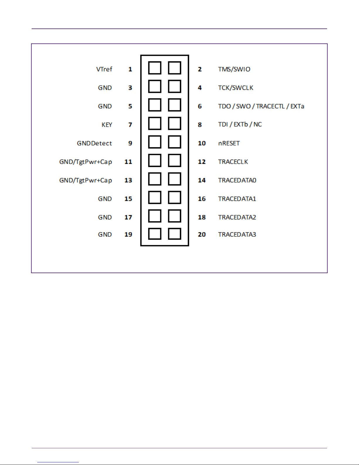
Some newer ARM microcontroller board use a 0.05” 20-pin header (Samtec FTSH-110) for both debug and trace. (The signals
greyed out are not available on the Cortex-M3 or Cortex-M4.) The 20-pin Cortex Debug D ETM connector support both JTAG and
Serial Wire debug protocols. When the Serial debug protocol is used, the TDO signal can be used for Serial Wire Viewer output
for trace capture. The connector also provides a 4-bit wide trace port for capturing of trace that require a higher trace bandwidth
(example, when ETM trace is enabled).
Hardware Design Guidelines for S32K1xx Microcontrollers , Rev. 3, December 2018
Application Note
6 / 33
Page 7
NXP Semiconductors
Debug and programing interface
Figure 4. 20-pin Cortex Debug D ETM connector pin layout
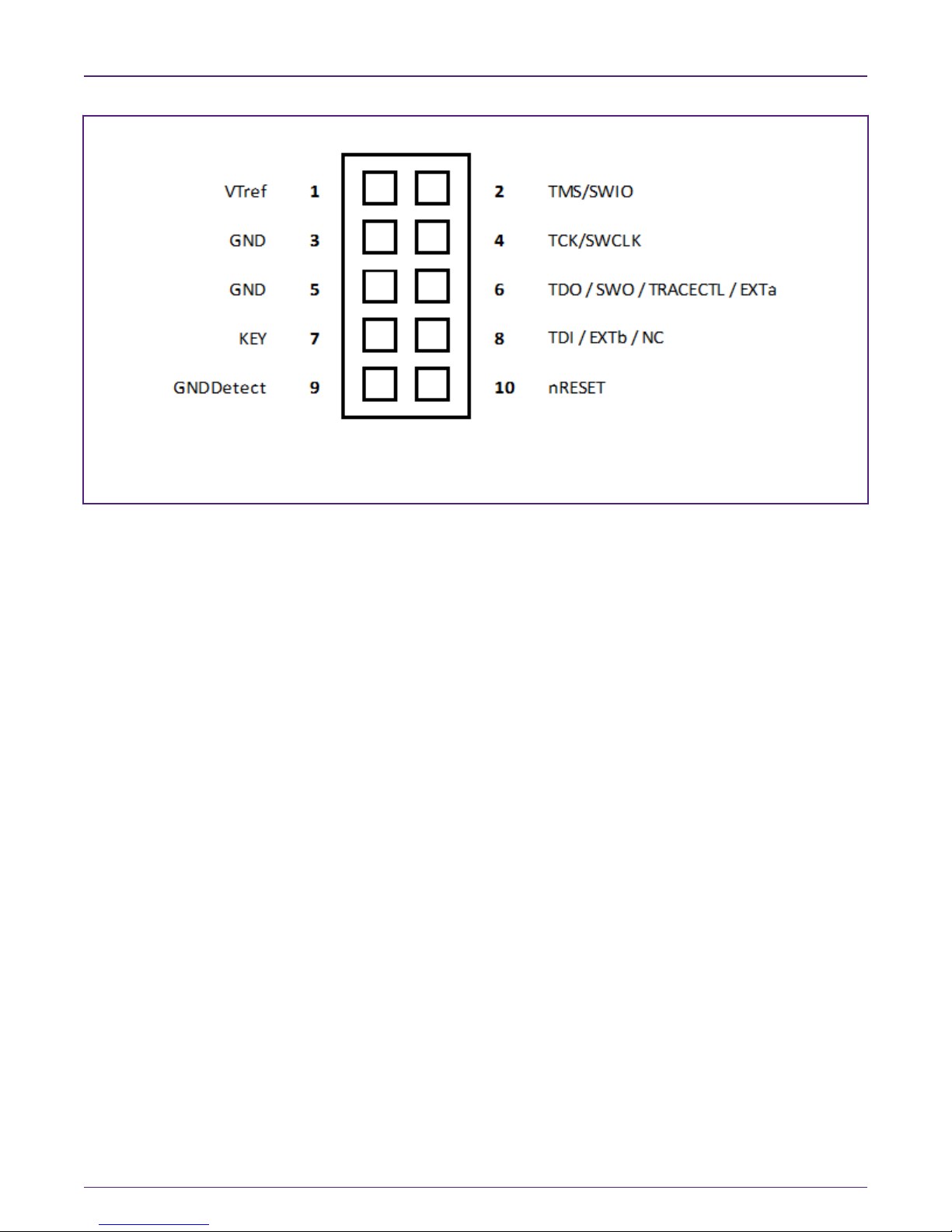
5.1.2 10-pin Cortex Debug connector
For device without ETM, you can use an even smaller 0.05” 10-pin connector (Samtec FTSH-105) for debug. Similar to the 20pin Cortex Debug D ETM connector, both JTAG and Serial-Wire debug protocols are supported in the 10-pin version.
Hardware Design Guidelines for S32K1xx Microcontrollers , Rev. 3, December 2018
Application Note
7 / 33
Page 8
NXP Semiconductors
Figure 5. 10-pin Cortex Debug connector pin layout
Debug and programing interface
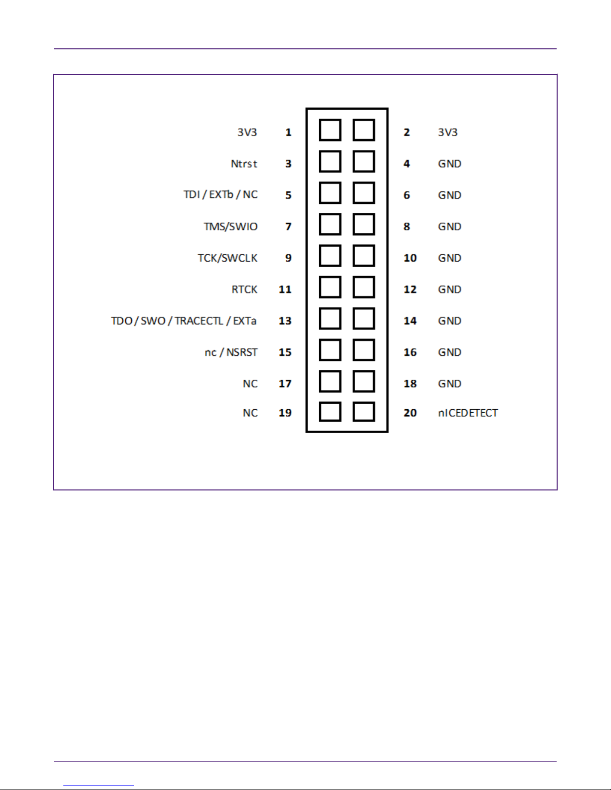
5.1.3 Legacy 20-pin IDC connector
A common debug connector used in ARM development boards is the 20-pin IDC connector. The 20-pin IDC connector arrange
support JTAG debug, Serial Wire debug (SWIO and SWCLK), Serial Wire Output (SWO). The nICEDETECT pin allows the target
system to detect if a debugger is connected. When no debugger is attached, this pin is pulled high. A debugger connection
connects this pin to ground. This is used in some development boards that support multiple JTAG con- figurations. The nSRST
connection is optional; debugger can reset a Cortex-M system via the System Control Block (SCB) so this connection is often
omitted from the top level of microcontroller designs.
Hardware Design Guidelines for S32K1xx Microcontrollers , Rev. 3, December 2018
Application Note
8 / 33
Page 9
NXP Semiconductors
Debug and programing interface
Figure 6. 20-pin IDC connector
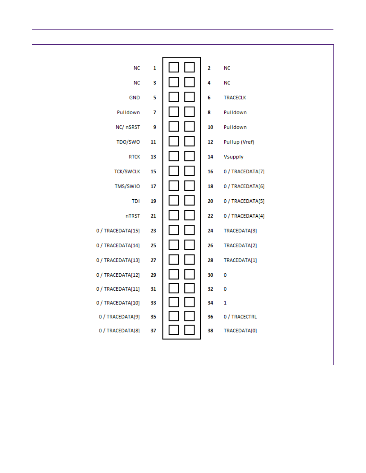
5.1.4 38-pin Mictor connector
In some ARM system designs, Mictor connector is used when trace port is required (example, for instruction trace with ETM). It
can also be used for JTAG/SWD connection. The 20-pin IDC connector can be connected in parallel with the Mictor connector
(only one is use at a time).
Hardware Design Guidelines for S32K1xx Microcontrollers , Rev. 3, December 2018
Application Note
9 / 33
Page 10
NXP Semiconductors
Debug and programing interface
Figure 7. 38-pin Mictor connector
Typically a Cortex-M3 or Cortex-M4 microcontroller only has 4-bit of trace data signals, so most of the trace data pins on the Mictor
connectors are not used. The Mictor connector is used mostly in other ARM Cortex processors (CortexA8/A9, Cortex-R4) or in
some multiprocessor systems the trace system might require a wider trace port. In such cases, some of the other unused pins
on the connector will also be used. For a typical Cortex-M3 or Cortex-M4 system, the Cortex Debug D ETM connector is
recommended.
Hardware Design Guidelines for S32K1xx Microcontrollers , Rev. 3, December 2018
Application Note
10 / 33
Page 11

NXP Semiconductors
Analog comparator interface
5.2 RESET system
Resetting the MCU provides a way to start processing from a known set of initial conditions. System reset begins with the on-chip
regulator in full regulation and system clocking generation from an internal reference.
5.2.1 External pin RESET
For all reset sources, the RESET_B pin is driven low by the MCU for at least 128 bus clock cycles and until flash memory
initialization has completed.
After flash memory initialization has completed, the RESET_B pin is released and the internal chip reset desserts. Keeping the
RESET_B pin asserted externally delays the negation of the internal chip reset.
On this device, RESET is a dedicated pin. This pin is open drain and has an internal pull/up device. Asserting RESET wakes the
device from any mode. During a pin reset, the RCM's SRS[PIN] bit is set. Hence, application software can detect an external pin
RESET by reading this register.
In case RESET_PIN_CFG within Flash Option Register (FTFC_FOPT) is cleared, RESET_B pin is disabled following a POR and
cannot be enabled as reset function. When this option is selected, there could be a short period of contention during a POR ramp
where the device drives the pin low prior to establishing the setting of this option and releasing the reset function on the pin. The
RESET pin is the same as the standard GPIO. It can operate as a pseudo open-drain output because there is also a PMOS
device in the output stage.
This bit is preserved through system resets and low-power modes. When RESET_B pin function is disabled, it cannot be used
as a source for low-power mode wake-up.
NOTE
When the reset pin has been disabled and security has been enabled by means of the FSEC register, a mass
erase can be performed only by setting both the Mass Erase and System Reset Request fields in the MDM-AP
register.
The reset line has an internal pull-up resistor. If the environment and the customer application is noisy, an external pull up resistor
(between 10KOhmshms-100KOhms) can be added and to avoid a sporadic or unintended reset occurs. Refer to the device
datasheet for the value of the internal pull-up resistor value.
Despite a capacitor in the reset line is not directly required for the MCU. In some cases, in order to add a further ESD protection,
an external capacitor is added between the RESET pin to ground. The values of the pull up resistor and the capacitor must be
selected according to the design requirements of the application. Refer to the device datasheet for the minimum RESET pulse
value that can be detected for the MCU.
Analog comparator interface
6
The comparator (CMP) module provides a circuit for comparing two analog input voltages in the S32K1xx Microcontrollers. The
comparator circuit is designed to operate across the full range of the supply voltage, known as rail-to-rail operation. CMPO is high
when the non-inverting input is greater than the inverting input, and is low when the non-inverting input is less than the inverting
input.
Hardware Design Guidelines for S32K1xx Microcontrollers , Rev. 3, December 2018
Application Note
11 / 33
Page 12

NXP Semiconductors
Analog comparator interface
Figure 8. General windowed timing diagram
Figure 9. CMP high level diagram
The switching of the high-speed interfaces or any GPIO may introduce some noise to the analog or comparator inputs due to
inductance/capacitive coupling between the MCU pins. The cross-talk may be introduced by PCB tracks that run close to each
Hardware Design Guidelines for S32K1xx Microcontrollers , Rev. 3, December 2018
Application Note
12 / 33
Page 13

NXP Semiconductors
Communication modules
other or that cross each other. In order to avoid and mitigate the high-frequency noise and any coupling. Please ensure that the
analog comparator input signal impedance is 50K or less.(see Figure 9. on page 12)
Figure 10. Shielding of analog signals
Placing ground planes and shapes alongside sensitive analog signals provides shielding on the PCB. Care should be taken to
minimize the length of the paths of these types of signal on the PCB. This prevents interference and I/O cross-talk affecting the
signal. The large amount of metal has the lowest possible resistance and lowest possible inductance because of the large, flattened
conductor pattern. The ground plane acts as a low-impedance return path for decoupling high-frequency currents caused by fast
digital logic. It also minimizes emissions from electromagnetic interference/radio-frequency interference (EMI/RFI). In other hand,
the ground planes also permit high-speed digital or analog signals to be transmitted via transmission-line (microstrip or stripline)
techniques, where controlled impedances are required.
Communication modules
7
7.1 LIN interface for LPUART module
The Local Interconnect Network (LIN) is a serial communication protocol, designed to support automotive networks. As the lowest
level of a hierarchical network, LIN enables cost-effective communication with sensors and actuators when all the features of CAN
are not required.
Features of the LPUART module supports and include:
• LIN master and slave operation
• Full-duplex, standard non-return-to-zero (NRZ) format
• Programmable baud rates (13-bit modulo divider) with configurable oversampling ratio from 4x to 32x
• Transmit and receive baud rate can operate asynchronous to the bus clock:
— Baud rate can be configured independently of the bus clock frequency
— Supports operation in Stop modes
Hardware Design Guidelines for S32K1xx Microcontrollers , Rev. 3, December 2018
Application Note
13 / 33
Page 14

NXP Semiconductors
• Interrupt, DMA or polled operation:
— Transmit data register empty and transmission complete
— Receive data register full
— Receive overrun, parity error, framing error, and noise error
— Idle receiver detect
— Active edge on receive pin
— Break detect supporting LIN
— Receive data match
• Hardware parity generation and checking
• Programmable 7-bit, 8-bit, 9-bit or 10-bit character length
• Programmable 1-bit or 2-bit stop bits
• Three receiver wakeup methods:
— Idle line wakeup
— Address mark wakeup
— Receive data match
Communication modules
• Automatic address matching to reduce ISR overhead:
— Address mark matching
— Idle line address matching
— Address match start, address match end
• Optional 13-bit break character generation / 11-bit break character detection
• Configurable idle length detection supporting 1, 2, 4, 8, 16, 32, 64 or 128 idle characters
• Selectable transmitter output and receiver input polarity
• Hardware flow control support for request to send (RTS) and clear to send (CTS) signals
• Selectable IrDA 1.4 return-to-zero-inverted (RZI) format with programmable pulse width
• Independent FIFO structure for transmit and receive
— Separate configurable watermark for receive and transmit requests
Option for receiver to assert request after a configurable number of idle characters if receive FIFO is not empty.
Table 4. LPUART signal description
Signal Description I/O
TXD Transmit data. This pin is normally an
I/O
output, but is an input (tristated) in
single wire mode whenever the
transmitter is disabled or transmit
direction is configured for receive data.
RXD Receive data. I
CTS_B Clear to send. I
RTS_B Request to send. O
Hardware Design Guidelines for S32K1xx Microcontrollers , Rev. 3, December 2018
Application Note
14 / 33
Page 15

NXP Semiconductors
Communication modules
The LIN bus topology utilizes a single master and multiple nodes, as shown below. Connecting application modules to the vehicle
network makes them accessible for diagnostics and service.
Figure 11. LIN bus topology
The LIN transmitter is a low-side MOSFET with current limitation and overcurrent transmitter shutdown. A selectable internal pullup resistor with a serial diode structure is integrated, so no external pull-up components are required for the application in a slave
node. To be used as a master node, an external resistor of 1 kΩ in series with a diode must be placed in parallel between VBAT
[Battery Voltage] and the LIN Bus line. The fall time from recessive to dominant and the rise time from dominant to recessive is
selectable and controlled to guarantee communication quality and reduce EMC emissions.
Figure 12. Circuit diagram for LIN interface
Hardware Design Guidelines for S32K1xx Microcontrollers , Rev. 3, December 2018
Application Note
15 / 33
Page 16

NXP Semiconductors
7.1.1 LIN components data
Table 5. LIN components
Reference Part Mounting Remark
Communication modules
DMLIN
RML1 and RML2
C1
Diode Mandatory only for master
ECU
Resistor: 2 kΩ
Power Loss: 250 mW
Mandatory only for Master
ECU
Tolerance: 1%
Package Size: 1206
Requirement:
Min Power rating of the
complete master termination
has to be ≥ 500 mW
Capacitor:
Mandatory
Slave ECU: typically 220 pF
Master ECU: from 560 pF up
to approximately ten times that
value in the slave node
[CSLAVE], so that the total line
capacitance is less dependent
on the number of slave nodes.
Reverse Polarity protection
from LIN to VSUP.
For Master ECU
If more than 2 resistors are
used in parallel, the values
have to be chosen in a way
that the overall resistance RM
of 1 kΩ and the minimum
power loss of the complete
master termination has to be
fulfilled.
For Slave ECU
RMLIN1 and RMLIN2 are not
needed on the PCB layout
The value of the master node
has to be chosen in a way that
the LIN specification is fulfilled.
C2
ESD1
Tolerance: 10%
Package Size: 0805
Voltage: ≥50 V
Capacitor:
Package Size: 0805
ESD Protection
Package Size: 0603-0805
Optional Mounting of the optional part
only allowed if there is an
explicit written permission of
the respective OEM available.
Place close to the connector.
Optional
Layout pad for an additional
ESD protection part.
Mounting of the optional part
only allowed if there is an
explicit written permission of
the respective OEM available.
Place close to the connector.
Hardware Design Guidelines for S32K1xx Microcontrollers , Rev. 3, December 2018
Application Note
16 / 33
Page 17

NXP Semiconductors
Communication modules
7.2 CAN interface for FlexCAN module
The physical layer characteristics for CAN are specified in ISO-11898-2. This standard specifies the use of cable comprising
parallel wires with an impedance of nominally 120 Ω (95 Ω as minimum and 140 Ω as maximum). The use of shielded twisted
pair cables is generally necessary for electromagnetic compatibility (EMC) reasons, although ISO-11898-2 also allows for
unshielded cable. A maximum line length of 40 meters is specified for CAN at a data rate of 1 Mb. However, at lower data rates,
potentially much longer lines are possible. ISO-11898-2 specifies a line topology, with individual nodes connected using short
stubs.
Though not exclusively intended for automotive applications, CAN protocol is designed to meet the specific requirements of a
vehicle serial data bus: real-time processing, reliable operation in the EMI environment of a vehicle, cost-effectiveness, and
required bandwidth.
Each CAN station is connected physically to the CAN bus lines through a transceiver device. The transceiver is capable of driving
the large current needed for the CAN bus and has current protection against defective CAN or defective stations. A typical CAN
system with an S32K1xx microcontroller is shown in Figure 13. on page 17
Figure 13. CAN system
The FlexCAN module is a full implementation of the CAN protocol specification, the CAN with Flexible Data rate (CAN FD) protocol
and the CAN 2.0 version B protocol, which supports both standard and extended message frames and long payloads up to 64
bytes transferred at faster rates up to 8 Mbps. The message buffers are stored in an embedded RAM dedicated to the FlexCAN
module. See the chip configuration details in the Reference Manual for the number of message buffers configured in the chip.
Like most others CAN physical transceivers, the CANH, CANL and SPLIT pins are available for the designer to terminate bus
depending on the application. The Figure 14. on page 18 and Figure 15. on page 18 show examples of the CAN node
terminations.
Hardware Design Guidelines for S32K1xx Microcontrollers , Rev. 3, December 2018
Application Note
17 / 33
Page 18

NXP Semiconductors
Communication modules
Figure 14. CAN physical transceiver circuit
Figure 15. CAN physical transceiver circuit with common mode choke
Hardware Design Guidelines for S32K1xx Microcontrollers , Rev. 3, December 2018
Application Note
18 / 33
Page 19

NXP Semiconductors
7.2.1 CAN components data
Table 6. CAN components
Reference Description
Denotes a guard track next to a high/medium speed track.
Guard tracks are connected such that each end of the track is
connected to ground. A guard track should be connected to
the ground plane at least every 500 mils. Spacing from any
protected conductor and the guard track must not exceed 20
mils.
Communication modules
CBUS1 and CBUS2
Z1 and Z2
RTERM1,
RTERM2 and CCOM1
LBUS1–Common mode choke
The Capacitors CBUS1 and CBUS2 are not specifically
required. They may be added for EMC reasons, in which
case the maximum capacitance from either bus wire to
ground must not exceed 300 pF total. If zener stacks are also
needed, the parasitic capacitance of the zener stacks must
also be included in the total capacitance budget.
The zener stacks Z1 and Z2 could be required to satisfy
Automotive EMC requirements (ESD in particular). These
devices should be placed close to the connector.
Depending on the position of the node within the CAN network
it might need a specific termination. RTERM1, RTERM2 and
CCOM1 must be that they assist in having an overall cable
impedance. On a bus implementation of a CAN network only
the two nodes on the two ends of the bus have terminator
resistors. The nodes not placed on the end of the CAN bus do
not have termination. A thorough analysis is required to
maintain this requirement of the CAN networks.
The SPLIT pin on the transceiver is optional and the designer
might choose not to use it. This pin helps stabilize the recessive
state of the CAN bus and can be enabled or disabled by
software when required.
A common mode choke on the CANH and CANL lines can
help reduce coupled electromagnetic interference and
needed to satisfy Automotive EMC requirements. This choke,
together with transient suppressors on the transceiver pins
can greatly reduce coupled electromagnetic noise, and highfrequency transients. LBUS1 is not specifically required.
7.2.2 CAN termination
In a transmission line, there are two current paths, one to carry the currents from the driver to the receiver and another to provide
the return path back to the driver. In the CAN transmission lines is more complex because there are two signals that are sharing
a common termination as well as a ground return path. For reliable CAN communications, it is essential that the reflections in the
transmission line be kept as small as possible. This can only be done by proper cable termination. Figure 16. on page 20 and
Figure 17. on page 20 demonstrates two CAN termination schemes.
Reflections happen very quickly during and just after signal transitions. On a long line, the reflections are more likely to continue
long enough to cause the receiver to misread logic levels. On short lines, the reflections occur much sooner and have no effect
on the received logic levels.
Hardware Design Guidelines for S32K1xx Microcontrollers , Rev. 3, December 2018
Application Note
19 / 33
Page 20

NXP Semiconductors
Communication modules
7.2.2.1 Parallel termination
In CAN applications, both ends of the bus must be terminated because any node on the bus may transmit/receive data. Each end
of the link has a termination resistor equal to the characteristic impedance of the cable, although the recommended value for the
termination resistors is nominally 120 Ω (100 Ω as minimum and 130 Ω as maximum).
There should be no more than two terminating resistors in the network, regardless of how many nodes are connected, because
additional terminations place extra load on the drivers. ISO-11898-2 recommends not integrating a terminating resistor into a
node, but rather attaching standalone termination resistors at the furthest ends of the bus. This is to avoid a loss of a termination
resistor if a node containing that resistor is disconnected. The concept also applies to avoiding the connection of more than two
termination resistors to the bus, or locating termination resistors at other points in the bus rather than at the two ends.
Figure 16. d CAN Bus - parallel termination
7.2.2.2 Parallel termination with common-mode filtering
To further enhance signal quality, split the terminating resistors at each end in two and place a filter capacitor, CSPLIT, between
the two resistors. This filters unwanted high frequency noise from the bus lines and reduces common-mode emissions.
Figure 17. CAN Bus – parallel transmission with common-mode filtering
7.3 Inter-Integrated Circuit IIC
The Inter-Intergrated Circuit (IIC) bus is a two-wire, bidirectional serial bus that provides a simple, efficient method of data exchange
between devices. Being a two-wire device, the IIC bus minimizes the need for large numbers of connections between devices,
and eliminates the need for an address decoder. This bus is suitable for applications requiring occasional communications over
a short distance between a number of devices. It also provides flexibility, allowing additional devices to be connected to the bus
Hardware Design Guidelines for S32K1xx Microcontrollers , Rev. 3, December 2018
Application Note
20 / 33
Page 21

NXP Semiconductors
Communication modules
for further expansion and system development. Both SDA and SCL are bidirectional lines, connected to a positive supply voltage
via a pull-up resistor (see Figure 18. on page 21. When the bus is free, both lines are high. The output stages of devices
connected to the bus must have an open-drain or open collector in order to perform the wired-AND function. The interface is
designed to operate up to 100 kbps with maximum bus loading and timing. The device is capable of operating at higher baud
rates, up to a maximum of clock/20, with reduced bus loading. The maximum communication length and the number of devices
that can be connected are limited by a maximum bus capacitance of 400 pF.
Figure 18. Connection of I2C-bus devices to the I2C-bus
Hardware Design Guidelines for S32K1xx Microcontrollers , Rev. 3, December 2018
Application Note
21 / 33
Page 22

NXP Semiconductors
Communication modules
Figure 19. Maximum value of RP as a function of bus capacitance for a standard-mode I2C-bus
7.4 Ethernet MAC Interface
MII/RMII Interface signal can be directly routed to the MAC-NET interface, however series termination resistors may be considerate
on RXCLK, TXCLK and all RX/TX signals for EMI suppression. MII/RMII series termination should be placed within 100 of the
Ethernet Physical Interface and routed to an uninterrupted reference plane. 33-50 Ohms series termination resistors have been
to be good recommended value for improving EMI.
Although RMII and MII are synchronous bus architectures, there are a number of factors limiting signal trace lengths. With a longer
trace, the signal becomes more attenuated at the destination and thus more susceptible to noise interference. Longer traces also
act as antennas, and if run on the surface layer, can increase EMI radiation. If a long trace is running near and adjacent to a noisy
signal, the unwanted signals could be coupled in as cross talk. It is recommended to keep the signal trace lengths as short as
possible. Ideally, keep the traces under 6 inches. Trace length matching, to within 2.0 inches on the MII or RMII bus is also
recommended. Significant differences in the trace lengths can cause data timing issues. Minimize the use of vias throughout the
design. Vias add capacitance to signal traces. As with any high-speed data signal, good design practices dictate that impedance
should be maintained and stubs should be avoided throughout the entire data path.
MII signaling: Figure 20. on page 23 shows the PHY-MAC and MAC-MAC connections in an MII interface. Data is exchanged
via 4-bit wide data nibbles TXD[3:0] and RXD[3:0]. Data transmission is synchronous with the transmit (TX_CLK) and receive
(RX_CLK) clocks. For the PHY-MAC interface, both clock signals are provided by the PHY and are typically derived from an
Hardware Design Guidelines for S32K1xx Microcontrollers , Rev. 3, December 2018
Application Note
22 / 33
Page 23

NXP Semiconductors
Quad Serial Peripheral Interface
external crystal running at a nominal 25 MHz or from the CLK_OUT signal on the switch. When the Ethernet Switch is configured
for MAC-MAC communication, the switch provides the clocks and acts like a PHY.
Figure 20. MII interface connections
RMII signaling: RMII data is exchanged via 2-bit data signals TXD[1:0] and RXD[1:0] as shown in Figure 21. on page 23.
Transmit and receive signals are synchronous with the shared reference clock, REF_CLK.
Figure 21. RMII interface connections
8 Quad Serial Peripheral Interface
S32K1xx has one instance of QuadSPI. The Quad Serial Peripheral Interface (QuadSPI) block acts as an interface to external
serial flash device. It supports SDR and HyperRAM modes upto 4 and 8 bidirectional data lines respectively. The QuadSPI
supports an A-side and a B-side. The A-side of the QuadSPI is connected to the fast pads (80 mA) while the B-side connects to
the 20 mA pads. See datasheet for operating values.
Only one external memory will be supported in any given application and it will not be permitted to run the A-side and the B-side
of the QuadSPI simultaneously. As such the following external memory options can be supported:
• Single Quad Flash on the A-side
Hardware Design Guidelines for S32K1xx Microcontrollers , Rev. 3, December 2018
Application Note
23 / 33
Page 24

NXP Semiconductors
Figure 22. External memory option - Single Quad Flash on the A-side
Quad Serial Peripheral Interface
• Single HyperRAM on the B-side
Figure 23. External memory option - Single HyperRAM on the B-side
• Single Quad Flash on the B-side.
Hardware Design Guidelines for S32K1xx Microcontrollers , Rev. 3, December 2018
Application Note
24 / 33
Page 25

NXP Semiconductors
Figure 24. External memory option - Single Quad Flash on the B-side
Quad Serial Peripheral Interface
Data and Clock Signal Termination: Clock generation and distribution becomes more difficult as the speed and performance
of microprocessors increase to higher limits. Controlled and precise clocking distribution techniques are needed to maintain a
synchronous system. Clock signal quality and skew are the two major problems with distributing clock signals. With higher
frequencies, and the associated fast edge rates, long traces behave like transmission lines. Ring back, overshoot, and undershoot
occur as a result of poor termination of transmission lines. They contribute to bad signal quality, false switching, and they can
cause damage in extreme cases.
Given the effective output driver strength of 25-33 Ohms and the transmission line characteristic impedance of 50 Ohms, one
should add the termination resistor close to the output driver, to minimize the reflection as shown below.
Figure 25. Point-To-Point transmission line
Data Signal Routing: In order to keep the correct timing for the data transfer from the Microcontroller to the IC Memory, the PCB
data traces should be the same length and time delay as the clock trace from Microcontroller to the IC Memory. Data signals
should be routed with controlled impedance traces to reduce signal reflections. Avoid routing traces with 90 ° angle corners. The
recommendation is to cut the corner and smooth the trace when a trace route needs to change direction. To further improve the
Hardware Design Guidelines for S32K1xx Microcontrollers , Rev. 3, December 2018
Application Note
25 / 33
Page 26

NXP Semiconductors
Unused pins
signal integrity, avoid using multiple signal layers for data signal routing. All signal traces should have a continuous and solid
reference plane, either GND or VDD.
Clock Signal Routing: In high speed synchronous data transfer, good signal integrity in a PCB design is of critical importance,
especially for the clock signals, SCLK and DQS. When routing the clock signal, special cares should be taken. The following
practices are recommended.
• Run the clock signal at least -w3w of the trace width away from all other signal traces. This helps keep the clock signal clean
from crosstalk noise.
• Use as few via(s) as possible for the whole clock signal path. Vias cause impedance change and signal reflection.
• All signal traces should go with a solid reference plane, either GND or VCC.
• Run the clock trace as straight as possible and avoid using serpentine routing.
• Keep a continuous ground in the next layer as reference plane.
• Route the clock trace with controlled impedance.
• Keep the clock signal from disturbance or crosstalk by separating it from other signals by using wider spacing. Data bus
should be routed with matching length to the reference of the clock. The matching length is recommended to be within ± 50
mils.
Figure 26. Recommended clock signal routing
9 Unused pins
The unused digital and analog pins must be left floating. In software, the application should ensure that the ports function of the
MCU is 'DISABLED'. The DISABLED function is default state for all pins not initialized.
Hardware Design Guidelines for S32K1xx Microcontrollers , Rev. 3, December 2018
Application Note
26 / 33
Page 27

NXP Semiconductors
General board layout guidelines
10 General board layout guidelines
10.1 Traces recommendations
A right angle in a trace can cause more radiation. The capacitance increases in the region of the corner and the characteristic
impedance changes. This impedance change causes reflections. Avoid right-angle bends in a trace and try to route them with at
least two 45° corners. To minimize any impedance change, the best routing would be a round bend, as shown in Figure 27. on
page 27.
Figure 27. Poor and correct way of bending traces in right angles
To minimize crosstalk, not only between two signals on one layer but also between adjacent layers, route them 90° to each other.
Complex boards need to use vias while routing; you have to be careful when using them. These add additional capacitance and
inductance, and reflections occur due to the change in the characteristic impedance. Vias also increase the trace length. While
using differential signals, use vias in both traces or compensate the delay in the other trace.
10.2
Grounding techniques apply to both multi-layer and single-layer PCBs. The objective of grounding techniques is to minimize the
ground impedance and thus to reduce the potential of the ground loop from circuit back to the supply.
Grounding
• Route high-speed signals above a solid and unbroken ground plane.
• Do not split the ground plane into separate planes for analog, digital, and power pins. A single and continuous ground
plane is recommended.
• There should be no floating metal/shape of any kind near any area close to the microcontroller pins. Fill copper in the
unused area of signal planes and connect these coppers to the ground plane through vias.
Hardware Design Guidelines for S32K1xx Microcontrollers , Rev. 3, December 2018
Application Note
27 / 33
Page 28

NXP Semiconductors
General board layout guidelines
Figure 28. Eliminating floating metal/shape
10.3 EMI/EMC and ESD considerations for layout
These considerations are important for all system and board designs. Though the theory behind this is well explained, each board
and system experiences this in its own way. There are many PCB and component related variables involved.
This application note does not go into the electromagnetic theory or explain the whys of different techniques used to combat the
effects, but it considers the effects and solutions most recommended as applied to CMOS circuits. EMI is radio frequency energy
that interferes with the operation of an electronic device. This radio frequency energy can be produced by the device itself or by
other devices nearby. Studying EMC for your system allows testing the ability of your system to operate successfully counteracting
the effects of unplanned electromagnetic disturbances coming from the devices and systems around it. The electromagnetic noise
or disturbances travels via two media: Conduction and Radiation.
Hardware Design Guidelines for S32K1xx Microcontrollers , Rev. 3, December 2018
Application Note
28 / 33
Page 29

NXP Semiconductors
Figure 29. Electromagnetic noise propagation
General board layout guidelines
The design considerations narrow down to:
• The radiated & conducted EMI from the board should be lower than the allowed levels by the standards you are following.
• The ability of the board to operate successfully counteracting the radiated & conducted electromagnetic energy (EMC)
from other systems around it.
The EMI sources for a system consists of several components such as PCB, connectors, cables and so on. The PCB plays a
major role in radiating the high frequency noise. At higher frequencies and fast-switching currents and voltages, the PCB traces
become effective antennas radiating electromagnetic energy; e.g., a large loop of signal and corresponding ground. The five main
sources of radiation are: digital signals propagating on traces, current return loop areas, inadequate power supply filtering or
decoupling, transmission line effects, and lack of power and ground planes. Fast switching clocks, external buses and PWM
signals are used as control outputs and in switching power supplies. The power supply is another major contributor to EMI. RF
signals can propagate from one section of the board to another building up EMI. Switching power supplies radiate the energy
which can fail the EMI test. This is a huge subject and there are many books, articles and white papers detailing the theory behind
it and the design criteria to combat its effects.
Every board or system is different as far as EMI/EMC and ESD issues are concerned, requiring its own solution.
However, the common guidelines to reduce an unwanted generation of electromagnetic energy are as shown below:
• Ensure that the power supply is rated for the application and optimized with decoupling capacitors.
• Provide adequate filter capacitors on the power supply source. The bulk/bypass and decoupling capacitors should have
low equivalent series inductance (ESL).
• Create ground planes if there are spaces available on the routing layers. Connect these ground areas to the ground plane
with vias.
• Keep the current loops as small as possible. Add as many decoupling capacitors as possible. Always apply current return
rules to reduce loop areas.
• Keep high-speed signals away from other signals and especially away from input and output ports or connectors.
Hardware Design Guidelines for S32K1xx Microcontrollers , Rev. 3, December 2018
Application Note
29 / 33
Page 30

NXP Semiconductors
PCB layer stacking
11 PCB layer stacking
To reach signal integrity and performance requirements, at minimum a four-layer PCB is recommended for implementing Ethernet
applications and systems. The following layer stack-ups are recommended for four, six, and eight-layer boards, although other
options are possible.
Figure 30. Recommended PCB layer stack-up
Hardware Design Guidelines for S32K1xx Microcontrollers , Rev. 3, December 2018
Application Note
30 / 33
Page 31

NXP Semiconductors
Injection current
12 Injection current
All pins implement protection diodes that protect against electrostatic discharge (ESD). In many cases, both digital and analog
pins need to be connected to voltages that are higher than the operating voltage of the device pin. In addition to providing protection
from ESD, these diode structures will also clamp the voltage to a diode drop above the supply of that pin segment. This is
permissible, as long as the current injection is limited as defined in the device specification. Current can be limited by adding a
series resistor on the signal. The input protection diodes will keep the voltage at the pin to a safe level (per the absolute maximum
ratings of the device) as long as it is less than the maximum injection current specification.
For more reference see AN4731.
Figure 31. Input protection circuit for I/O port
13 References
• Crystal Oscillator Troubleshooting Guide - NXP Semiconductors
• AN2049 Some Characteristics and Design Notes for Crystal Feedback ...
• AN10853 ESD and EMC sensitivity of IC - NXP Semiconductors
• AN2321: Designing for Board Level Electromagnetic Compatibility - NXP Semiconductors
• AN10897 A guide to designing for ESD and EMC
Revision history
14
Table 7. Sample revision history
Revision number Date Substantive changes
0 03/2017 Initial release
Table continues on the next page...
Hardware Design Guidelines for S32K1xx Microcontrollers , Rev. 3, December 2018
Application Note
31 / 33
Page 32

NXP Semiconductors
Table 7. Sample revision history (continued)
Revision number Date Substantive changes
Revision history
1 06/2017
2
02/2018
1. In Table 1. Power domains and decoupling
capacitors on page 2 Footnote is added in the table
2. In Clock circuitry on page 3 the value of Fast
internal reference clock is changed to 48MHz from
48-60MHz and value of External square wave input
clock changed to 50 MHz from 60 MHz
3. In #unique_8/
unique_8_Connect_42_TABLE_WGL_5ZD_CZ
deleted the line (if not .........by MCU)
4. External pin RESET on page 11 changed from
When the RESET................. drain output to The
RESET pin....................output stage
5. In Power supplies on page 2 Figure 1. on page 2
updated.
6. In Clock circuitry on page 3 When using the
external oscillator....the frequency range of the
external oscillator should be 4–40 MHz changed to
8–40 MHz
7. New chapter Analog comparator interface on page
11 added
1. Updated the table Table 1. Power domains and
decoupling capacitors on page 2.
3 12/2018
2. Added the following sections Quad Serial
Peripheral Interface on page 23, Injection current
on page 31, PCB layer stacking on page 30,
Ethernet MAC Interface on page 22
1. Updated Figure 1. on page 2
2. In Debug and programing interface on page 5
removed the text "
Usually, MCUs do not include pull-up or pull-down
resistors on JTAG/SWD pins".
3. In External pin RESET on page 11 removed the
paragraph "In prototype designs.......330 pF are
recommended" and added "The reset line has
an ......pull-up resistor value" and "Despite a
capacitor in.....detected for the MCU".
4. Removed the column "Required pull-up / pulldown"
from Table 3. JTAG signal description on page 6.
5. In External pin RESET on page 11 removed the
figure "RESET circuit".
6. Updated Unused pins on page 26 and added a
note.
Hardware Design Guidelines for S32K1xx Microcontrollers , Rev. 3, December 2018
Application Note
32 / 33
Page 33

How To Reach Us
Home Page:
nxp.com
Web Support:
nxp.com/support
Information in this document is provided solely to enable system and software implementers to
use NXP products. There are no express or implied copyright licenses granted hereunder to
design or fabricate any integrated circuits based on the information in this document. NXP
reserves the right to make changes without further notice to any products herein.
NXP makes no warranty, representation, or guarantee regarding the suitability of its products for
any particular purpose, nor does NXP assume any liability arising out of the application or use
of any product or circuit, and specifically disclaims any and all liability, including without limitation
consequential or incidental damages. “Typical” parameters that may be provided in NXP data
sheets and/or specifications can and do vary in different applications, and actual performance
may vary over time. All operating parameters, including “typicals,” must be validated for each
customer application by customer's technical experts. NXP does not convey any license under
its patent rights nor the rights of others. NXP sells products pursuant to standard terms and
conditions of sale, which can be found at the following address: nxp.com/
SalesTermsandConditions.
NXP, the NXP logo, NXP SECURE CONNECTIONS FOR A SMARTER WORLD, COOLFLUX,
EMBRACE, GREENCHIP, HITAG, I2C BUS, ICODE, JCOP, LIFE VIBES, MIFARE, MIFARE
CLASSIC, MIFARE DESFire, MIFARE PLUS, MIFARE FLEX, MANTIS, MIFARE ULTRALIGHT,
MIFARE4MOBILE, MIGLO, NTAG, ROADLINK, SMARTLX, SMARTMX, STARPLUG, TOPFET,
TRENCHMOS, UCODE, Freescale, the Freescale logo, AltiVec, C‑5, CodeTEST, CodeWarrior,
ColdFire, ColdFire+, C‑Ware, the Energy Efficient Solutions logo, Kinetis, Layerscape, MagniV,
mobileGT, PEG, PowerQUICC, Processor Expert, QorIQ, QorIQ Qonverge, Ready Play,
SafeAssure, the SafeAssure logo, StarCore, Symphony, VortiQa, Vybrid, Airfast, BeeKit,
BeeStack, CoreNet, Flexis, MXC, Platform in a Package, QUICC Engine, SMARTMOS, Tower,
TurboLink, and UMEMS are trademarks of NXP B.V. All other product or service names are the
property of their respective owners. ARM, AMBA, ARM Powered, Artisan, Cortex, Jazelle, Keil,
SecurCore, Thumb, TrustZone, and μVision are registered trademarks of ARM Limited (or its
subsidiaries) in the EU and/or elsewhere. ARM7, ARM9, ARM11, big.LITTLE, CoreLink,
CoreSight, DesignStart, Mali, mbed, NEON, POP, Sensinode, Socrates, ULINK and Versatile are
trademarks of ARM Limited (or its subsidiaries) in the EU and/or elsewhere. All rights reserved.
Oracle and Java are registered trademarks of Oracle and/or its affiliates. The Power Architecture
and Power.org word marks and the Power and Power.org logos and related marks are trademarks
and service marks licensed by Power.org.
©
NXP B.V. 2018. All rights reserved.
For more information, please visit: http://www.nxp.com
For sales office addresses, please send an email to: salesaddresses@nxp.com
Date of release: December 2018
Document identifier: AN5426
 Loading...