

Page 1

3-Phase Sensorless BLDC Motor
Control Development Kit with S12
MagniV MC9S12ZVML128 MCU
Quick Start Guide
Page 2
Quick Start Guide
3-Phase Sensorless BLDC
Motor Control Development Kit with
S12 MagniV MC9S12ZVML128 MCU
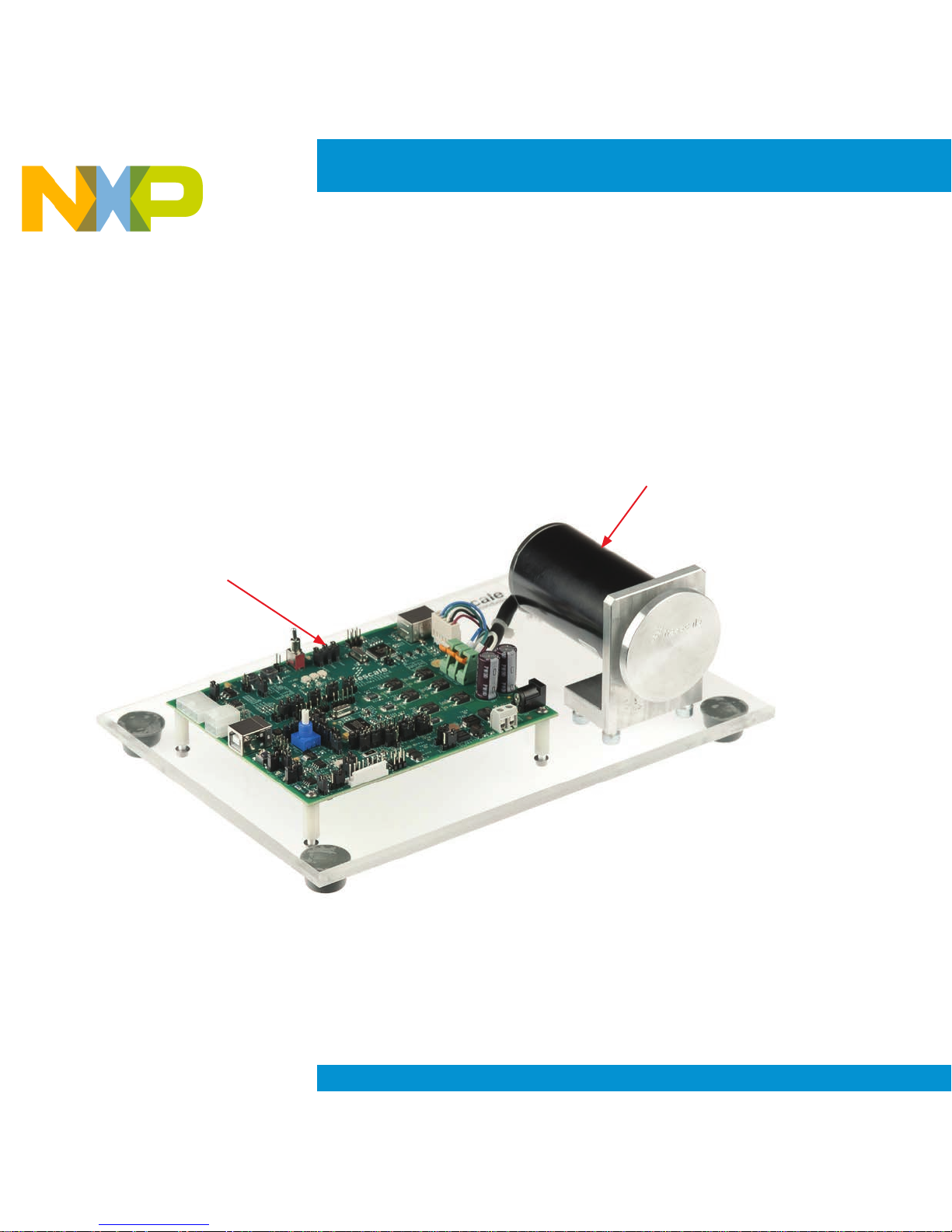
S12 MagniV
MC9S12ZVML128
Evaluation Board
3-Phase
BLDC Motor
Page 3

3-Phase Sensorless BLDC
Motor Control Development Kit with
S12 MagniV MC9S12ZVML128 MCU
Hardware
• S12 MagniV MC9S12ZVML128
evaluation board with integrated
3-phase 12 V/10 A power stage
• 3-phase BLDC motor with Hall
sensor, 24 VDC, 9350 RPM, 90 W,
45ZWN24-90-B
• USB cable
• 12 VDC power supply
Resources
• Sensorless control using back EMF
zero-crossing detection application
source code
• Automotive math and motor
control library set for MC9S12ZVM
installation package
• FreeMASTER installation pack
• FreeMASTER project
• 3-phase sensorless BLDC kit with
MC9S12ZVML128 MCU quick start
guide
• 3-phase sensorless BLDC kit with
MC9S12ZVML128 MCU fact sheet
• 3-phase sensorless BLDC kit with
MC9S12ZVML128 MCU application
note AN4704
• MC9S12ZVML128 evaluation board
user guide
Page 4
Quick Start Guide
4
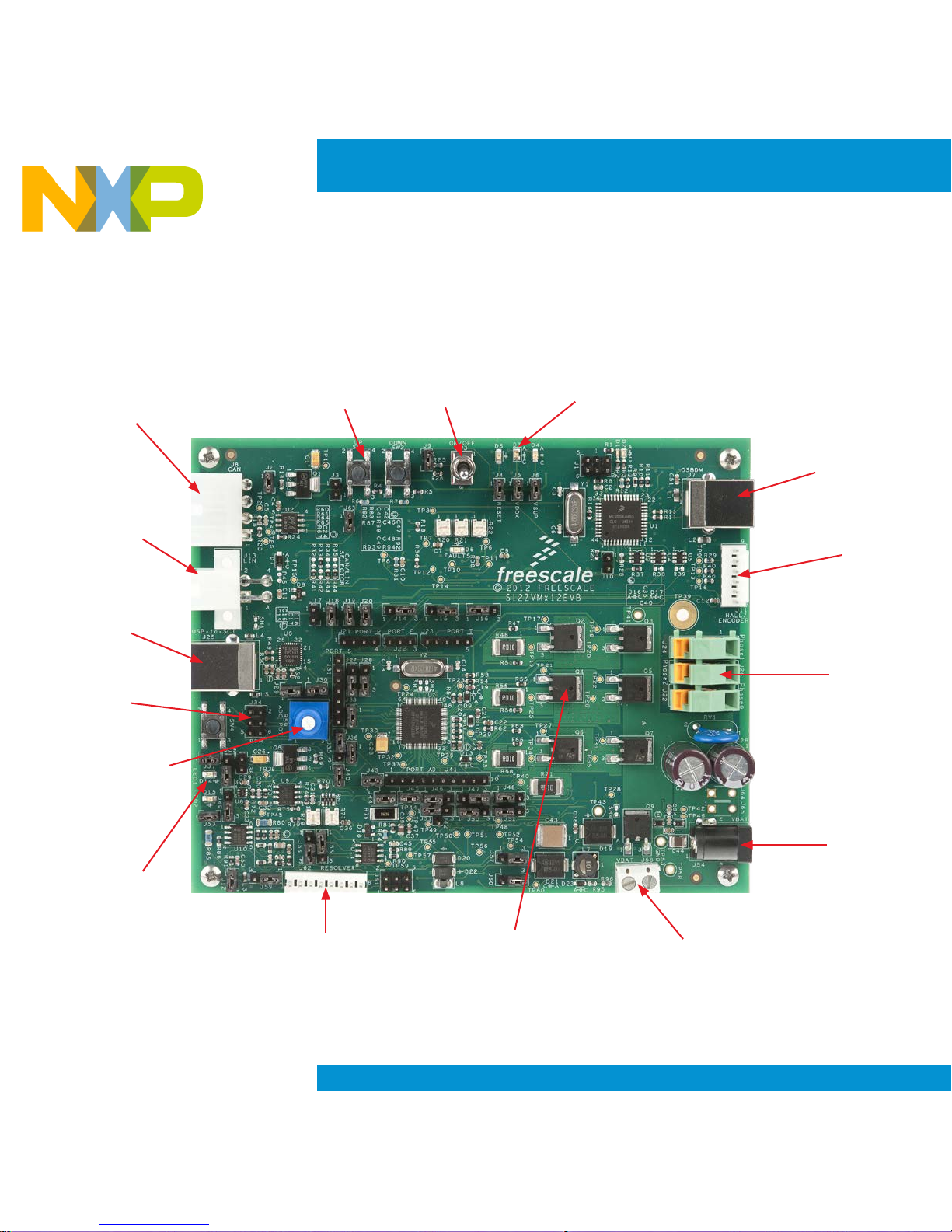
S12 MagniV MC9S12ZVML128
Evaluation Board
User
Buttons
User
Switch
Power
Indicator
LEDs
OSBDM
Hall/
Encoder
Interface
Motor
Power
Supply
Power
Supply
Terminal
6x Power
MOSFETs
Resolver
Interface
User LEDs
Potentiometer
Routed to
ADC Input
BDM
Interface
Freemaster
USB-to-SCI
Interface
LIN
Connector
CAN
Option
Page 5

5
1
Install the FreeMASTER debugging
tool. Download the application at
freescale.com/freemaster.
2
Install the CP210x virtual COM port
driver. The CP210x virtual COM
port driver installation file is available
in the “Downloads” section at
freescale.com/automcdevkits.
3
Run “Device Manager” on your
system and check which COM port
was assigned to the CP210x COM
port driver.
4
Connect the MC9S12ZVML128
evaluation board and the host PC
via the supplied USB cable.
5
Connect the power supply to the
MC9S12ZVML128 evaluation board.
Please ensure the development kit is updated
with the latest available application software
found at freescale.com/automcdevkits before
proceeding to step 6.
Software Tools Installation
6
Start the FreeMASTER project
MC9S12ZVML128_BLDC_
Sensorless.pmp located in
MTRCKTSBNZVM128\SW\
MC9S12ZVML128_BLDC_
Sensorless project directory.
7
Enable communication by pressing
the “STOP” button in the
FreeMASTER, or by pressing
“CTRL+K.”
8
Successful communication is
signalized in the status bar. If the
communication is not established,
check the USB connection between
the PC and MC9S12ZVML128
evaluation board, communication
port and speed. The
communication port and speed can
be set in the Project\Options menu
(or pressing “CTRL+T”). The
communication speed must be set
at 9600 Bd.
Page 6

Quick Start Guide
6
1
When the power supply is
connected to EVB board, the BLDC
motor is in stop mode. The user
switch starts the motor.
2
The application is controlled
by user controls built into
MC9S12ZVML128 evaluation board
or by the FreeMASTER interface.
3
Enter the required speed by
changing the value of the “Required
Speed RPM” variable in the
variables watch window or by
double clicking the speed gauge in
the “Control Page.” The “Required
Speed RPM” variable is scaled in
revolutions per minute.
Application Control
4
Analyze behavior of BLDC motor
during transients by opening
“Speed Scope.” Speed Scope
displays scope of “Actual Speed
RPM” and “Required Speed RPM”
variables.
5
Change the maximum allowed
value of DC bus current by
modifying “DC bus Current Limit” in
the variables watch window.
Page 7

7
Jumper Option Setting Description
J2
CAN
Transceiver 5 V
supply option
Open VDDC ballast transistor is not supplied from VSUP
Close VDDC ballast transistor is supplied from VSUP
J3
VDDC supplied
from USB
option
Open
VDDC node is not supplied from the USB-to-SCI
interface
Close
VDDC node is supplied from the USB-to-SCI
interface
J4
RESET LED
indicator option
Open RESET LED indicator disabled
Close RESET LED indicator enabled
J5
VDDX LED
indicator option
Open VDD LED indicator disabled
Close VDD LED indicator enabled
J6
VSUP LED
indicator option
Open VSUP LED indicator disabled
Close VSUP LED indicator enabled
S12 MagniV MC9S12ZVML128
Evaluation Board Jumper Options
The following is a list of all jumper options. The default installed jumper settings are
shown in white text within the blue boxes.
Page 8

Quick Start Guide
8
J9
ON/OFF switch
option
Open ON/OFF switch disabled
Close ON/OFF switch enabled
J10
OSBDM boot-
loader option
Open OSBDM boot loader disabled
Close OSBDM boot loader enabled
J12
Resolver circuit
5 V supply
option
Open Resolver input circuitry (+5VDC) supply disabled
Close Resolver input circuitry (+5VDC) supply enabled
J14
EVDD or FAULT
selector
1-2 FAULT input is connected to port PP0
2-3
Port PP0 is connected to EVDD at Hall sensor
interface
J15
Resolver or
Hall/encoder
phase A
selector
1-2 Phase A from resolver is connected to port PT1
2-3
Phase A from Hall/encoder interface is connected
to port PT1
J16
Resolver or
Hall/encoder
phase B
selector
1-2
Phase B from Hall/encoder interface is connected
to port PT2
2-3 Phase B from resolver is connected to port PT2
Jumper Options
Continued
Jumper Option Setting Description
Page 9

9
J18
USB-to-SCI
interface supply
option
Open USB-to-SCI isolator supply disable
Close USB-to-SCI isolator supply enable
J19
“UP” push-
button option
Open “UP” push button disabled
Close “UP” push button enabled
J20
“DOWN” push-
button option
Open “DOWN” push button disabled
Close “DOWN” push button enabled
J27
SCI RXD
selector
1-2 RXD from OSBDM is connected to port PS2
2-3 RXD from USB-to-SCI is connected to port PS2
J28
SCI TXD
selector
1-2 TXD from OSBDM is connected to port PS3
2-3 TXD from USB-to-SCI is connected to port PS3
J29
BDM interface
supply option
Open BDM supply disabled
Close BDM supply enabled
Jumper Options
Continued
Jumper Option Setting Description
Page 10

Quick Start Guide
10
J30
ADC
potentiometer
pull-up option
Open POT 1 (ADC potentiometer) supply disabled
Close POT 1 (ADC potentiometer) supply enabled
J33
MCU supply
option
Open MCU supply disabled
Close MCU supply enabled
J35
ADC mapping
PAD0
1-2
Connects PAD0 to AMP0 external gain-setting
resistors
2-3 Connects PAD0 to POS_SIN resolver output
J36
VREF
generation
supply option
Open
Disconnects VSUP to supply a regulated voltage
at VREF2
Close
Connects VSUP to supply a regulated voltage at
VREF2
J37
USER LED1
option
Open “User LED1” disabled
Close “User LED1” enabled
J38 PDO-PDOCLK
Open PDO-PDOCLK not shorted
Close PDO-PDOCLK shorted
Jumper Options
Continued
Jumper Option Setting Description
Page 11

11
J39
Resolver phase
B selector
1-2
SINCOS I/O connector phase B connected to
resolver phase B input
2-3 POS_COS connected to resolver phase B input
J40
VDDX ballast
supply option
Open VDDX ballast is disconnected
Close VDDX ballast is connected
J43
Resolver circuit
12 V supply
option
Open Resolver generator circuit supply disconnected
Close Resolver generator circuit supply connected
J44
ADC mapping
PAD1
Open
PAD1 is disconnected from the AMPM0 external
gain-setting resistors
Close
PAD1 is connected to the AMPM0 external gainsetting resistors
J45
ADC mapping
PAD2
Open
PAD2 is disconnected from the AMPP0 external
gain-setting resistors
Close
PAD2 is connected to the AMPP0 external gainsetting resistors
Jumper Options
Continued
Jumper Option Setting Description
Page 12

Quick Start Guide
12
J46
ADC mapping
PAD3
1-2
Connects PAD3 to ADC_IA (phase A current
sense from external opamp)
2-3 Connects PAD3 to POS_SIN resolver output
J47
ADC mapping
PAD4
1-2
Connects PAD4 to ADC_IB (phase B current
sense from external opamp)
2-3 Connects PAD4 to ADC potentiometer POT1
J48
ADC mapping
PAD5
1-2
Connects PAD5 to AMP1 external gain setting
resistors
2-3
Connects PAD5 to ADC_IB (phase B current
sense from external opamp)
J49
Resolver phase
A selector
1-2
Resolver phase A connected to SINCOS I/O
connector phase A input
2-3
Resolver phase A connected to resolver POS_SIN
Schmitt-Trigger
J50
ADC mapping
PAD6
1-2
Connects PAD6 to AMPM1 external gain-setting
resistors
2-3 Connects PAD6 to POS_COS resolver output
Jumper Options
Continued
Jumper Option Setting Description
Page 13

13
J51/J42
ADC mapping
PAD7
J51(1-2)
Connects PAD7 to AMPP1 external gain-setting
resistors
J51(2-3) Connects PAD7 to POS_SIN resolver output
J42(1)-J51(2) Connects PAD7 to ADC potentiometer POT1
J52
ADC mapping
PAD8
1-2
Connects PAD8 to ADC_IC (phase C current
sense from external opamp)
2-3 Connects PAD8 to POS_COS resolver output
J53
USER LED2
option
Open “User LED 2” disabled
Close “User LED 2” enabled
J55 VREF selector
1-2 VREF supplied from VDDX
2-3 VREF supplied from the VREF2 regulator
J56
Resolver COS
reference
1-2 Input to POS_COS circuit is from OFFSET1
2-3 Input to POS_COS circuit is from RES_COS_REF
Jumper Options
Continued
Jumper Option Setting Description
Page 14

Quick Start Guide
14
J57
Internal AMP0
input selector
(inverting)
1-2
Connects DC bus to the internal AMP0 inverting
input (phase A current sense)
2-3
Connects ground to the internal AMP0 inverting
input (DC bus current sense)
J59
Resolver SIN
reference
1-2 Input to POS_SIN circuit is from RES_SIN_REF
2-3 Input to POS_SIN circuit is from OFFSET1
J60
Internal AMP0
input selector
(non-inverting)
1-2
Connects phase A to the internal AMP0 noninverting input (phase A current sense)
2-3
Connects DC bus as non-inverting input for
internal AMP0 (DC bus current sense)
J63
FAULT
comparators
5 V supply
option
Open FAULT circuit supply disconnected
Close FAULT circuit supply connected
Jumper Options
Continued
Jumper Option Setting Description
Page 15

15
S12 MagniV MC9S12ZVML128 Evaluation
Board Jumper Position
FreeMASTER
USB-to-SCI
Interface
J18
J27
J28
J29
J38
J37
J53
User Buttons User Switch
BDM
Interface
User
LEDs
DC Bus Current
Sense
J35 J44 J45 J60 J57
J19 J20
J9
Page 16

For more information, visit
freescale.com/automcdevkits
Freescale and the Freescale logo are trademarks of Freescale Semiconductor,
Inc., Reg. U.S. Pat. & Tm. Off. MagniV is a trademark of Freescale
Semiconductor, Inc. All other product or service names are the property of
their respective owners. © 2013 Freescale Semiconductor, Inc.a
Document Number: MTRCKTSBNZVM128QSG REV 0
Agile Number: 926-78779 REV A
Quick Start Guide
Support
Visit freescale.com/support for a list of phone
numbers within your region.
Warranty
Visit freescale.com/warranty for complete
warranty information.
 Loading...