

Page 1
Quick Start Guide
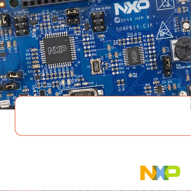
S08PB16-EVK
Page 2
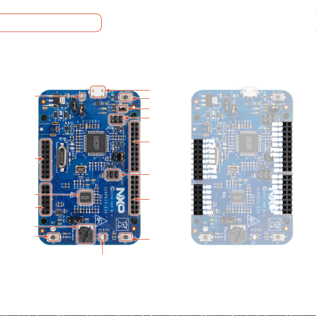
GET TO KNOW THE S08PB16-EVK
D6
J3
Header
S08PB16
J4
Header
Potentiometer
SW3
RGB LED
Power/OSBDM
Micro USB
SW1 Reset
J13
JM60 BDM
Header
J2 Header
PB16
P5V_MC_IN-16
BDM
Header
J1 Header
SW2
NC-2
P3V3-4
NC-6
P3V3-8
NC-10
GND-12
GND-14
NC-2
NC-4
NC-6
NC-8
NC-10
NC-12
1-PTA2
3-PTA1
5-PTB5
7-PTB4
9-PTC3
11-PTC2
13-PTC1
15-PTC0
1-NC
3-NC
5-NC
7-NC
9-NC
11-NC
NC-19
NC-17
NC-15
NC-13
NC-11
PTA3-9
PTB3-7
NC-5
NC-3
NC-1
NC-15
NC-13
NC-11
NC-9
NC-7
NC-5
PTA0--3
NC-1
20-NC
18-NC
16-NC
14-GND
12-NC
10-NC
8-NC
6-NC
4-NC
2-NC
16-NC
14-NC
12-NC
10-NC
8-NC
6-NC
4-NC
2-NC
Figure 1: S08PB16-EVK Callouts
Figure 2: S08PB16-EVK Pin-Outs
Page 3

www.nxp.com
STEP-BY-STEP INSTRUCTIONS
1. Connect the S08PB16-EVK to a PC using the included Micro USB cable to power/
OSBDM Micro USB connectors (J15) of S08PB16-EVK board. A green LED (D6) will
illuminate, indicating power is on.
2. The S08PB16-EVK comes pre-programmed with a demo to test the onboard RGB LED
(D8), potentiometer (R38) and buttons (SW2, SW3). First, turn on the power and the red
LED, blue LED and green LED will toggle once. Then, rotate the potentiometer (R38)
to the maximum resistance value. The LEDs will turn off. Next, press the two buttons
(SW2, SW3) separately to test the buttons. Lastly, the red LED will always toggle.
3. J11 is the BDM header which can be used to debug and program S08PB16 by the
debugger P&E Multilink FX or P&E Multilink.
4. J13 must be open when using P&E Multilink FX to supply power and
debug/program S08PB16.
5. Explore more out-of-box demos and download software and tools at
www.nxp.com/S08PB16-EVK.
Page 4

SUPPORT
Visit www.nxp.com/support for a list
of phone numbers within your region.
WARRANTY
Visit www.nxp.com/warranty for
complete warranty information.
software and documentation at
www.nxp.com/S08PB16-EVK.
Get Started
Download installation
www.nxp.com
NXP and the NXP logo are trademar ks of NXP B.V. All other product or service names are the proper ty of their
respective owners. ©2019 NXP B.V.
Document Number: S08PB16EVKQSG REV 1
Agile Number: 926-45786 Rev B
 Loading...