

Page 1

Freescale Semiconductor
Document Number: AN4034
Application Note
Qorivva MPC5643L Dual
Processor Mode
by: Mark Ruthenbeck
Applications Engineering
Microcontroller Solutions Group
Rev. 0, 03/2011
1 Scope
This paper is a brief tutorial and description on how to
select and run the MPC5643L in decoupled parallel
mode (DPM).
2 Reference material
Freescale document MPC5643LRM, MPC5643L
Microcontroller Reference Manual, Rev. 7, October
2010.
3 Overview
The paper reviews the dual core modes of the
MPC5643L, but focuses on the operation of the
decoupled parallel mode (DP mode or DPM) on the chip
and on how to enable the DPM.
The MPC5643L operates in both lock step mode and
DPM — this paper will focus on the DPM mode.
Contents
1 Scope . . . . . . . . . . . . . . . . . . . . . . . . . . . . . . . . . . . . . . . 1
2 Reference material . . . . . . . . . . . . . . . . . . . . . . . . . . . . . 1
3 Overview . . . . . . . . . . . . . . . . . . . . . . . . . . . . . . . . . . . . . 1
4 MPC5643L dual core architecture . . . . . . . . . . . . . . . . . . 2
4.1 Block diagram . . . . . . . . . . . . . . . . . . . . . . . . . . . . . 3
4.2 Sphere of replication . . . . . . . . . . . . . . . . . . . . . . . . 3
4.3 Memory map . . . . . . . . . . . . . . . . . . . . . . . . . . . . . . 3
5 Startup . . . . . . . . . . . . . . . . . . . . . . . . . . . . . . . . . . . . . . . 4
5.1 Hardware setup . . . . . . . . . . . . . . . . . . . . . . . . . . . . 4
5.2 Software setup . . . . . . . . . . . . . . . . . . . . . . . . . . . . 4
5.3 Basic dual core flash boot program flow . . . . . . . . . 5
6 Changing between LSM and DPM . . . . . . . . . . . . . . . . . 7
6.1 Configure the flash programming utility . . . . . . . . . . 7
6.2 Dump shadow flash to s-record file . . . . . . . . . . . . . 8
6.3 Modify s-record file to change LSM/DPM configuration
8
6.4 Program shadow flash with updated user configura-
tion. . . . . . . . . . . . . . . . . . . . . . . . . . . . . . . . . . . . . . 9
6.5 Verify new configuration . . . . . . . . . . . . . . . . . . . . . 9
7 Summary . . . . . . . . . . . . . . . . . . . . . . . . . . . . . . . . . . . . 10
8 Revision history . . . . . . . . . . . . . . . . . . . . . . . . . . . . . . . 10
© Freescale Semiconductor, Inc., 2011. All rights reserved.
Page 2

MPC5643L dual core architecture
4 MPC5643L dual core architecture
The MPC5643L, a SafeAssure solution, is a symmetrical dual core device based on Power Architecture™.
This device can run in one of two modes, lock step and decoupled parallel (DP) modes. The lock step mode
is for safety critical systems that require redundancy. The DP mode is for additional performance. The
increased performances possible in DP mode can be estimated in first approximation as about 1.6 the
performance of the LS mode at the same frequency.
In the DP mode, each CPU core and each connected channel run independently from the other one, and
redundancy checkers (RCCU) are disabled.
As you can see in the block diagram below, the core power architecture and core peripherals (DMA
controller, interrupt controller, crossbar bus system, memory protection unit, flash and RAM controllers,
peripheral bus bridge, system timers, and the watchdog timer) are replicated. This is referred to as the
sphere of replication.
This replication is one of the features that enables this chip to be used in a safety environment. In a dual
core mode, this replication adds a bit of additional programming for full operation.
Qorivva MPC5643L Dual Processor Mode, Rev. 0
Freescale Semiconductor 2
Page 3
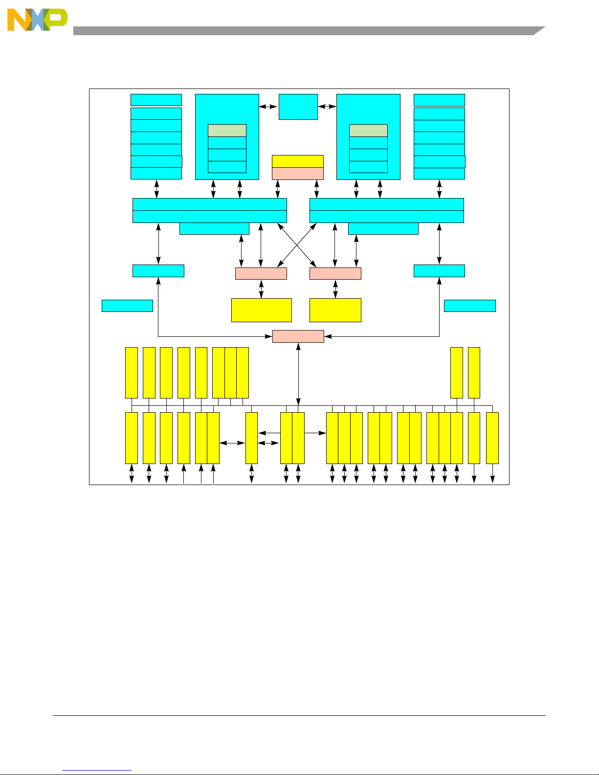
4.1 Block diagram
SRAM
PMU
SWT
ECSM
STM
INTC
DMA
Crossbar Switch
VLE
MMU
I-CACHE
SPE
e200z4
VLE
MMU
I-CACHE
SPE
e200z4
Memory Protection Unit
Crossbar Switch
Memory Protection Unit
AIPS Bridge
JTAG
Nexus
JTAG
Nexus
RC
RC
RC
RC
FlexRay
AIPS Bridge
TSENS T-Sens
ECC bits
Flash memory
ECC bits + logic
SIUL
MC
WakeUp
ADC
ADC
XOSC
BAM
SSCM
Secondary PLL
FMPLL
IRCOSC
CMU
CMU
CTU
PIT
FCCU
FlexPWM
FlexPWM
eTimer
eTimer
eTimer
FlexCAN
FlexCAN
LINFlex
LINFlex
DSPI
DSPI
DSPI CRC
CMU
SEMA4
PMU
SWT
ECSM
STM
INTC
DMA
SEMA4
SWG
ECC logic for SRAM ECC logic for SRAM
MPC5643L dual core architecture
4.2 Sphere of replication
The chip has two sets of peripherals around the core Power Architecture. With two sets of peripherals, the
software will need to initialize both sets of peripherals. This adds to the amount of code, but not necessarily
to the complexity of the code.
4.3 Memory map
If the system is in lock step mode, the sphere of replication peripherals have the identical memory map.
However, if the system is in dual processor mode, these same peripherals have unique addresses. On
core(0) the SoR peripherals remain at the LSM addresses, and the core(1) SoR peripherals are now visible
at a different set of addresses.
Qorivva MPC5643L Dual Processor Mode, Rev. 0
Freescale Semiconductor 3
Page 4
Startup
If in DP mode, the SRAM location is modified from lock step (LS) mode. In LS mode, there is 128 KB of
contiguous SRAM beginning at location 0x4000_0000. In DP mode, the memory is split into two 64 KB
areas, 0x4000_0000 to 0x4000_FFFF and 0x5000_0000 to 0x5000_FFFF.
All the peripherals that are not included in the SoR maintain their memory-mapped addresses. There is no
change of the addresses for the non-SoR peripherals.
5Startup
5.1 Hardware setup
The decision of which mode the chip runs (LSM and DPM) is determined by a user bit, LSM_DPM, in the
shadow sector of the flash. If this bit is 0, then the unit starts up in DP mode.
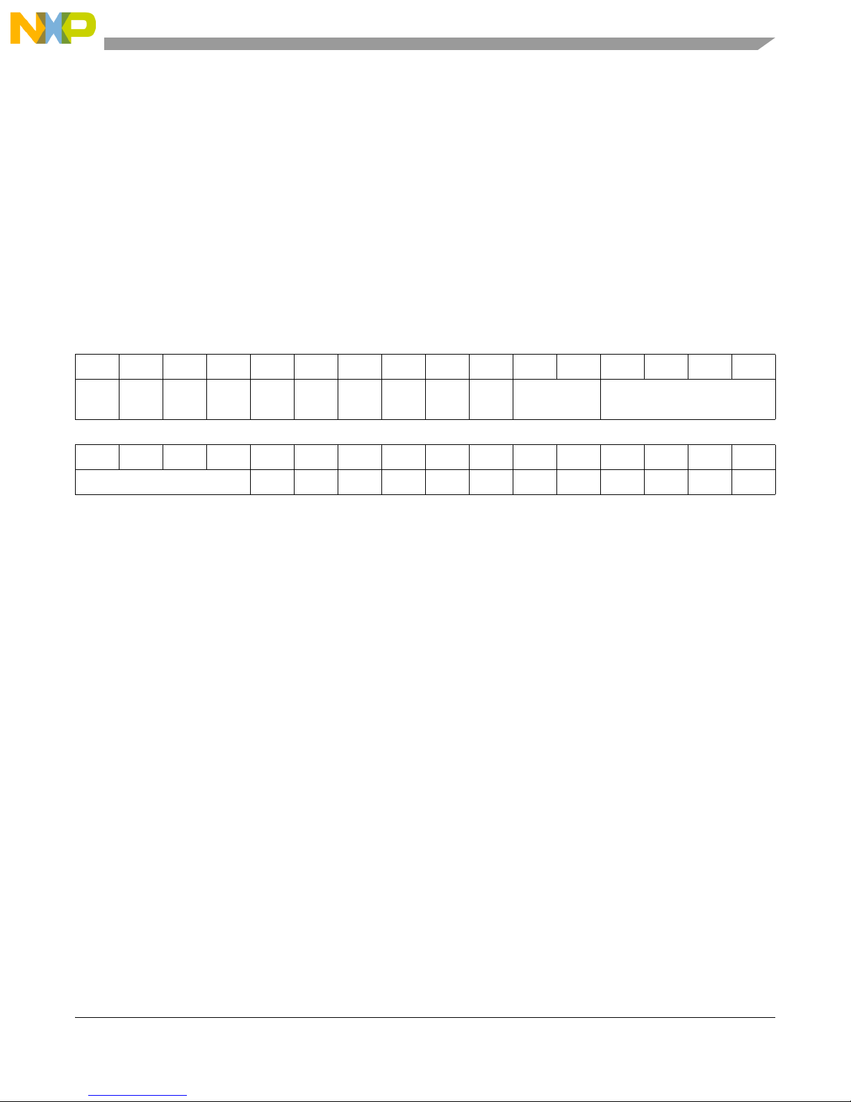
0123456789101112131415
SWT XOSC LSM_
DPM
16 17 18 19 20 21 22 23 24 25 26 27 28 29 30 31
Reserved
STCU Reserved
Figure 1. Shadow Flash — User Area
The shadow flash sector is located at 0x00F0_0000. The user configuration is located at offset 0x3E10.
This is also readable at flash register BIU4 (Flash_regs_base + 0x2C).
Refer to Section 6, “Changing between LSM and DPM” for detailed instructions on how to program the
shadow flash to switch between LSM and DPM.
5.2 Software setup
During the boot sequence, this dual core architecture is set up with one core being the master and the other
core designated as slave. That is to say, the primary core, Core(0), is run from reset and executes code,
which then sets up and releases reset to Core(1). At that time, the system then begins operating in dual
processor mode.
The System Status and Configuration Module (SSCM) is the control module for making the second core
operational. The registers of interest are:
• DPM Boot Register: Base + 0x0018
• Boot Key Register: Base + 0x001C
Qorivva MPC5643L Dual Processor Mode, Rev. 0
Freescale Semiconductor 4
Page 5

Startup
Address: Base + 0x0018 Access: Read/Write
0123456789101112131415
RP2BOOT
W
RESET: 0000000000000000
16 17 18 19 20 21 22 23 24 25 26 27 28 29 30 31
RP2BOOT
DVLE
W
RESET: 0000000000000000
= Writes have no effect on this bit
Figure 2. DPM Boot (DPMBOOT) Register
0
The reset vector is written into the DPM Boot Register[0:29]. Also, bit 30 is set to 1 to indicate that the
second core will be executing in VLE mode. If bit 30 is 0, then the core will operate in BookE mode. Bit
31 is don’t care.
Now that the boot vector is set up, to release reset of Core(1), two consecutive writes must be done to the
Boot Key Register (DPMKEY). The first write is 0x5AF0, the second is 0xA50F. When the second write
is complete, core(1) jumps to its reset vector.
5.3 Basic dual core flash boot program flow
For dual-core booting, the key concept to understand is that dual-core boot is nothing more than a typical
single-core boot, except that it starts another single-core boot. The initialization of interrupts, stack, etc.,
needs to be done on each core. So, it’s a single-core boot performed twice.
One point to remember is that an NMI is generated to both cores and this interrupt must be serviced
properly before the system runs both cores.
The diagram below shows a simplified boot process.
Qorivva MPC5643L Dual Processor Mode, Rev. 0
Freescale Semiconductor 5
Page 6

LSM_DPM=0
Boot in Lock Step
Mode
Core(0) MMU setup, other initialization
including NMI Vector, then branch to main().
Main() runs on Core(0), setting up the start
address for core(1) Place Reset Vector for
Core(1) in register P2BOOT.
Release Reset for Core(1) by writing
DPMKEY.
No
Core(1) runs MMU setup,other initialization
including NMI vector,
Power On Reset
Core(0) is now operational.
Core(1) changes the device mode from
DRUN to RUN0
FCCU Triggers NMI for both cores
Both cores manage their own NMI
Branch to Main()
Core(1) now operational
Core(1)
Core(0)
Startup
Qorivva MPC5643L Dual Processor Mode, Rev. 0
Freescale Semiconductor 6
Page 7

Changing between LSM and DPM
At power-on reset (POR), Core(0) begins operation while Core(1) remains held in reset. At this time,
Core(0) must initialize its set of peripherals, set up its environment (including the NMI routine), then
branch to main. At this point, Core(0) is essentially fully operational. Now Core(0) provides the reset
vector and writes the DMPKEY, thus releasing Core(1) from reset.
Core(1) begins its execution. The first thing that it must do is initialize its set of peripherals and set up its
environment, including its NMI routine. Core(1) then moves the chip from DRUN mode to RUN0 mode.
The system generates an NMI to both cores when the chip moves from DRUN to RUN0. Each core must
service its own NMI routines. Upon return from the NMI, both cores are now fully functional and
operating independently.
It is important for the NMI routines to be included, because the NMI interrupt is triggered when the system
moves to RUN mode.
6 Changing between LSM and DPM
As discussed in Section 5.1, “Hardware setup,” bit 9 at address 0x00F0_3E10 in the shadow flash
determines whether the cores operate in LS or DP mode. This section provides instructions on how to
program the shadow flash on the MPC5643L so that it can switch between LSM and DPM.
The following tools are required to perform the shadow flash programming:
• P&E ICDPPCNEXUS debugger for MPC55xx/56xx v1.23.3.2 or newer
• USB Multilink
6.1 Configure the flash programming utility
1. In the P&E tools installation folder, run the flash programming utility
...\pemicro\cw_progppcnexus.exe.
2. Ensure the MPC5643L is powered on and the USB Multilink is connected between the EVB and
the PC.
3. Select the Connect (Reset) to connect to the MPC5643L as shown in Figure 3.
Qorivva MPC5643L Dual Processor Mode, Rev. 0
Freescale Semiconductor 7
Page 8

Changing between LSM and DPM
Figure 3. Connecting to MPC5643L
4. Specify the programming algorithm to use. In this case, select the file from the P&E tools
installation folder
...\pemicro\algorithms\shadow\Freescale_MPC5643L_1x32x4k_Shadow_Blk_Freescale_C9
0FL2_Driver_031.PCP to enable program and erase operations on the shadow flash.
6.2 Dump shadow flash to s-record file
After the programming tool has been configured for the MPC5643L shadow flash, the existing contents of
the shadow flash should be dumped to an s-record file. The file will be used to change the configuration.
1. From the menu bar, select Upload Upload Module.
2. Specify a name for the s-record .s19 file.
6.3 Modify s-record file to change LSM/DPM configuration
The s-record file can now be edited to modify the LSM/DPM configuration. The s-record file format
S2xxyyyyyyzzzzcs is as follows:
•S2
Single-character start code S followed by a single-character record type. S2 indicates the line is a
data sequence with 3 bytes of address.
•xx
Two hexadecimal digits indicating the byte count in hexadecimal (address + data + checksum).
• yyyyyy
Six hexadecimal digits to indicate the three bytes of address that specify the memory location of
the first data byte
•zzzz
Zero to sixty-four pairs of hexadecimal characters specifying the data bytes
•cs
Two hex digits indicating the checksum, which is calculated by taking the sum of the all the bytes
Qorivva MPC5643L Dual Processor Mode, Rev. 0
Freescale Semiconductor 8
Page 9

Changing between LSM and DPM
from the byte count up to the last data byte, inclusive, modulo 256. This value is subtracted from
255 to obtain the checksum.
Example 1 shows an example s-record line at address 0x00FF_FE10. Note that this location is mirrored
with 0x00F0_3E10 which contains the user configuration discussed in Section 5.1, “Hardware setup.” The
s-record line has a byte count of 0x14, which includes a 3-byte address, 16-byte data section, and a 1-byte
checksum. The 32-bit user configuration contains 0xFFFFFFFF, which indicates bit 9 is set for LSM.
Example 1. Original S-record Line
S214FFFE10FFFFFFFFFFFFFFFFFFFFFFFFFFFFFFFFEE
In order to change the mode configuration to DPM, the s-record must be modified as shown in Example
2. Two changes are required: clear the LSM/DPM bit in the user configuration and recalculate the
checksum. To change to DPM, bit 9 of the user configuration is cleared so the new value is 0xFFBFFFFF.
This change requires the checksum to be recalculated as follows:
0xFF - [(0x14 + 0xFF + 0xFE + 0x10 + 0xFF + 0xBF + 0xFF + 0xFF + 0xFF + 0xFF + 0xFF + 0xFF +
0xFF + 0xFF + 0xFF + 0xFF+ 0xFF + 0xFF + 0xFF + 0xFF) mod 256] = 0x2E
Example 2. Modified S-record Line for DPM
S214FFFE10FFBFFFFFFFFFFFFFFFFFFFFFFFFFFFFF2E
The updated s-record file can now be used to program the shadow flash for DPM operation.
6.4 Program shadow flash with updated user configuration
Once the s-record file is updated, the MPC5643L shadow flash can be programmed with the new
configuration.
1. From the menu bar, select Program Erase Module.
2. From the menu bar, select File Specify Object File button and specify the name of the updated
s-record file.
3. From the menu bar, select Program Program Module button to download the s-record into the
shadow flash.
4. From the menu bar, select Verify Verify Module button to check the programming operation.
6.5 Verify new configuration
To verify the updated configuration:
1. Power-cycle the EVB to reset the MPC5643L in the new configuration.
2. Launch the P&E debugger from ...\pemicro\cw_icdppcnexus.exe and connect to the MPC5643L.
3. The status window shows the operating mode. Verify that the new mode is detected as shown in
Figure 4.
Qorivva MPC5643L Dual Processor Mode, Rev. 0
Freescale Semiconductor 9
Page 10

Summary
Figure 4. MPC5643L DPM detected
7Summary
Dual-core booting is nothing more than a typical single core boot with additional code that prepares the
second core for operation and releases it from reset. At that point the second core requires the same kind
of initialization code as used on the first core.
So the end result is really a single core with peripherals times two. There is no additional complexity of
code, only additional code.
8 Revision history
Table 1. Changes made April 2012
Section Description
Front page Add SafeAssure branding.
4 Add Qorivva branding.
Back page Apply new back page format.
1
No substantive changes were made to the content of this document; therefore the revision number was not
incremented.
1
Qorivva MPC5643L Dual Processor Mode, Rev. 0
Freescale Semiconductor 10
Page 11

How to Reach Us:
Home Page:
freescale.com
Web Support:
freescale.com/support
Information in this document is provided solely to enable system and software
implementers to use Freescale products. There are no express or implied copyright
licenses granted hereunder to design or fabricate any integrated circuits based on the
information in this document.
Freescale reserves the right to make changes without further notice to any products
herein. Freescale makes no warranty, representation, or guarantee regarding the
suitability of its products for any particular purpose, nor does Freescale assume any
liability arising out of the application or use of any product or circuit, and specifically
disclaims any and all liability, including without limitation consequential or incidental
damages. “Typical” parameters that may be provided in Freescale data sheets and/or
specifications can and do vary in different applications, and actual performance may
vary over time. All operating parameters, including “typicals,” must be validated for each
customer application by customer’s technical experts. Freescale does not convey any
license under its patent rights nor the rights of others. Freescale sells products
pursuant to standard terms and conditions of sale, which can be found at the following
address: http://www.reg.net/v2/webservices/Freescale/Docs/TermsandConditions.htm
Freescale, the Freescale logo, AltiVec, C-5, CodeTest, CodeWarrior, ColdFire, C-Ware,
Energy Efficient Solutions logo, Kinetis, mobileGT, PowerQUICC, Processor Expert,
QorIQ, Qorivva, StarCore, Symphony, and VortiQa are trademarks of Freescale
Semiconductor, Inc., Reg. U.S. Pat. & Tm. Off. Airfast, BeeKit, BeeStack, ColdFire+,
CoreNet, Flexis, MagniV, MXC, Platform in a Package, QorIQ Qonverge, QUICC
Engine, Ready Play, SafeAssure, SMARTMOS, TurboLink, Vybrid, and Xtrinsic are
trademarks of Freescale Semiconductor, Inc. All other product or service names are
the property of their respective owners.
The Power Architecture and Power.org
word marks and the Power and Power.org logos and related marks are
trademarks and service marks licensed by Power.org.
© 2011 Freescale Semiconductor, Inc.
Document Number: AN4034
Rev. 0
03/2011
 Loading...