


BB182
VHF variable capacitance diode
Rev. 03 — 24 February 2009 Product data sheet
1. Product profile
1.1 General description
The BB182 is a planar technology variable capacitance diode in a SOD523 (SC-79)
ultra small plastic package. The excellent matching performance is achieved by gliding
matching and a Direct Matching Assembly (DMA) procedure.
1.2 Features
n High linearity
n Excellent matching to 2 % DMA
n Ultra small plastic SMD package
n C
n Low series resistance
d(28V)
: 2.7 pF; C
d(1V)
to C
d(28V)
ratio: 22
1.3 Applications
n Electronic tuning in VHF television tuners, Band A up to 160 MHz
n Voltage Controlled Oscillators (VCO)
2. Pinning information
Table 1. Pinning
Pin Description Simplified outline Graphic symbol
1 cathode
2 anode
[1] The marking bar indicates the cathode.
3. Ordering information
Table 2. Ordering information
Type number Package
BB182 SC-79 plastic surface-mounted package; 2 leads SOD523
[1]
21
sym008
Name Description Version

NXP Semiconductors
4. Marking
Table 3. Marking codes
Type number Marking code
BB182 2
5. Limiting values
Table 4. Limiting values
In accordance with the Absolute Maximum Rating System (IEC 60134).
Symbol Parameter Conditions Min Max Unit
V
R
I
F
T
stg
T
j
BB182
VHF variable capacitance diode
reverse voltage - 32 V
peak value in series with a 10 kΩ resistor - 35 V
forward current - 20 mA
storage temperature −55 +150 °C
junction temperature −55 +125 °C
6. Characteristics
Table 5. Characteristics
Symbol Parameter Conditions Min Typ Max Unit
I
R
r
s
C
d
C
d(1V)/Cd(2V)
C
d(1V)/Cd(28V)
C
d(25V)/Cd(28V)
∆C
d/Cd
reverse current see Figure 2
=30V - - 10 nA
V
R
=30V; Tj=85°C - - 200 nA
V
R
diode series resistance f = 100 MHz at Cd= 30 pF - 1.0 1.2 Ω
diode capacitance f = 1 MHz; see Figure 1 and
Figure 3
= 1 V 52 - 62 pF
V
R
= 28 V 2.48 2.7 2.89 pF
V
R
diode capacitance ratio (1 V to 2 V) f = 1 MHz - 1.31 diode capacitance ratio (1 V to 28 V) f = 1 MHz 20.6 22 diode capacitance ratio (25 V to 28 V) f = 1 MHz - 1.05 diode capacitance matching VR= 1 V to 28 V; in a sequence
--2%
of 10 diodes (gliding)
BB182_3 © NXP B.V. 2009. All rights reserved.
Product data sheet Rev. 03 — 24 February 2009 2 of 6

NXP Semiconductors
BB182
VHF variable capacitance diode
80
C
d
(pF)
60
40
20
0
−1
10
101
f = 1 MHz; Tj = 25 °C.
Fig 1. Diode capacitance as a function of reverse voltage; typical values
mlc816
10
TC
(K−1)
−3
d
I
(nA)
3
10
R
2
10
VR (V)
mbk439
mlc815
2
10
10
1
0 1008040 6020
T
(°C)
j
Fig 2. Reverse current as a function of junction
temperature; maximum values
−4
10
−5
10
−1
10
110
VR (V)
2
10
Tj = 0 °C to 85 °C.
Fig 3. Temperature coefficient of diode capacitance
as a function of reverse voltage; typical values
BB182_3 © NXP B.V. 2009. All rights reserved.
Product data sheet Rev. 03 — 24 February 2009 3 of 6
NXP Semiconductors
BB182
VHF variable capacitance diode
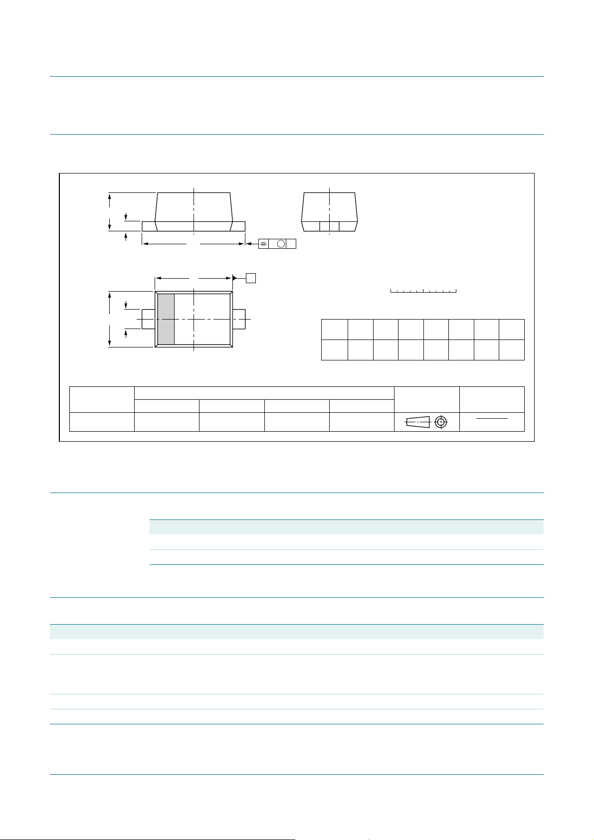
7. Package outline
Plastic surface-mounted package; 2 leads SOD523
A
c
v M
H
E
A
D
12
b
E
p
(1)
OUTLINE
VERSION
SOD523 SC-79
IEC JEDEC JEITA
Fig 4. Package outline SOD523 (SC-79)
8. Abbreviations
Table 6. Abbreviations
Acronym Description
SMD Surface-Mounted Device
VHF Very High Frequency
A
REFERENCES
0 0.5 1 mm
scale
DIMENSIONS (mm are the original dimensions)
UNIT b
Note
1. The marking bar indicates the cathode.
AH
0.65
mm
0.58
p
0.34
0.26
cD
0.17
1.25
0.11
1.15
EUROPEAN
PROJECTION
E
0.85
0.75
E
1.65
1.55
ISSUE DATE
02-12-13
06-03-16
v
0.1
9. Revision history
Table 7. Revision history
Document ID Release date Data sheet status Change notice Supersedes
BB182_3 20090224 Product data sheet - BB182_2
Modifications:
BB182_2 20041103 Product data sheet - BB182_1
BB182_1 19971113 Product specification - -
BB182_3 © NXP B.V. 2009. All rights reserved.
Product data sheet Rev. 03 — 24 February 2009 4 of 6
• The format of this data sheet has been redesigned to comply with the new identity
guidelines of NXP Semiconductors
• Legal texts have been adapted to the new company name where appropriate

NXP Semiconductors
10. Legal information
10.1 Data sheet status
BB182
VHF variable capacitance diode
Document status
Objective [short] data sheet Development This document contains data from the objective specification for product development.
Preliminary [short] data sheet Qualification This document contains data from the preliminary specification.
Product [short] data sheet Production This document contains the product specification.
[1] Please consult the most recently issued document before initiating or completing a design.
[2] The term ‘short data sheet’ is explained in section “Definitions”.
[3] The product status of device(s)described in this document mayhave changedsince this document was publishedand maydiffer incase of multipledevices. Thelatest product status
information is available on the Internet at URL
[1][2]
Product status
10.2 Definitions
Draft — The document is a draft version only. The content is still under
internal review and subject to formal approval, which may result in
modifications or additions. NXP Semiconductors does not give any
representations or warranties as to the accuracy or completeness of
information includedherein and shall have no liabilityfor the consequencesof
use of such information.
Short data sheet — A short data sheet is an extract from a full data sheet
with thesame product type number(s)and title. Ashort datasheet is intended
for quickreference only and should notbe relied upon to contain detailedand
full information. For detailed and full information see the relevant full data
sheet, which is available on request via the local NXP Semiconductors sales
office. In case of any inconsistency or conflict with the short data sheet, the
full data sheet shall prevail.
10.3 Disclaimers
General — Information in this document is believed to be accurate and
reliable. However,NXP Semiconductors does not giveany representations or
warranties, expressed or implied, asto the accuracy or completenessof such
information and shall have no liability for the consequences of use of such
information.
Right to make changes — NXP Semiconductors reserves the right to make
changes to information published in this document, including without
limitation specifications and product descriptions, at any time and without
notice. This documentsupersedes and replaces all information suppliedprior
to the publication hereof.
Suitability for use — NXP Semiconductors products are not designed,
authorized or warranted to be suitable for use in medical, military, aircraft,
space or life support equipment, nor in applications where failure or
[3]
http://www.nxp.com.
Definition
malfunction of an NXP Semiconductors product can reasonably be expected
to result in personal injury, death or severe property or environmental
damage. NXP Semiconductors accepts no liability for inclusion and/or use of
NXP Semiconductors products in such equipment or applications and
therefore such inclusion and/or use is at the customer’s own risk.
Applications — Applications that are described herein for any of these
products are for illustrative purposes only. NXP Semiconductors makes no
representation or warranty that such applications will be suitable for the
specified use without further testing or modification.
Limiting values — Stress above one or more limiting values (as defined in
the Absolute MaximumRatings System of IEC 60134) maycause permanent
damage tothedevice. Limiting valuesare stress ratings onlyand operation of
the device at these or any other conditions above those given in the
Characteristics sections of this document is not implied. Exposure to limiting
values for extended periods may affect device reliability.
Terms and conditions of sale — NXP Semiconductors products are sold
subject to the general terms and conditions of commercial sale, aspublished
at
http://www.nxp.com/profile/terms, including those pertaining to warranty,
intellectual property rights infringement and limitation of liability, unless
explicitly otherwise agreed to in writing by NXP Semiconductors. In case of
any inconsistency or conflict between information in this document and such
terms and conditions, the latter will prevail.
No offer to sell or license — Nothing in this document may be interpreted
or construed as an offer to sell products that is open for acceptance or the
grant, conveyance or implication of anylicense under any copyrights, patents
or other industrial or intellectual property rights.
10.4 Trademarks
Notice: Allreferenced brands,product names, service namesand trademarks
are the property of their respective owners.
11. Contact information
For more information, please visit: http://www.nxp.com
For sales office addresses, please send an email to: salesaddresses@nxp.com
BB182_3 © NXP B.V. 2009. All rights reserved.
Product data sheet Rev. 03 — 24 February 2009 5 of 6

NXP Semiconductors
12. Contents
1 Product profile . . . . . . . . . . . . . . . . . . . . . . . . . . 1
1.1 General description. . . . . . . . . . . . . . . . . . . . . . 1
1.2 Features . . . . . . . . . . . . . . . . . . . . . . . . . . . . . . 1
1.3 Applications . . . . . . . . . . . . . . . . . . . . . . . . . . . 1
2 Pinning information. . . . . . . . . . . . . . . . . . . . . . 1
3 Ordering information. . . . . . . . . . . . . . . . . . . . . 1
4 Marking. . . . . . . . . . . . . . . . . . . . . . . . . . . . . . . . 2
5 Limiting values. . . . . . . . . . . . . . . . . . . . . . . . . . 2
6 Characteristics. . . . . . . . . . . . . . . . . . . . . . . . . . 2
7 Package outline . . . . . . . . . . . . . . . . . . . . . . . . . 4
8 Abbreviations. . . . . . . . . . . . . . . . . . . . . . . . . . . 4
9 Revision history. . . . . . . . . . . . . . . . . . . . . . . . . 4
10 Legal information. . . . . . . . . . . . . . . . . . . . . . . . 5
10.1 Data sheet status . . . . . . . . . . . . . . . . . . . . . . . 5
10.2 Definitions. . . . . . . . . . . . . . . . . . . . . . . . . . . . . 5
10.3 Disclaimers. . . . . . . . . . . . . . . . . . . . . . . . . . . . 5
10.4 Trademarks. . . . . . . . . . . . . . . . . . . . . . . . . . . . 5
11 Contact information. . . . . . . . . . . . . . . . . . . . . . 5
12 Contents. . . . . . . . . . . . . . . . . . . . . . . . . . . . . . . 6
BB182
VHF variable capacitance diode
Please be aware that important notices concerning this document and the product(s)
described herein, have been included in section ‘Legal information’.
© NXP B.V. 2009. All rights reserved.
For more information, please visit: http://www.nxp.com
For sales office addresses, please send an email to: salesaddresses@nxp.com
Date of release: 24 February 2009
Document identifier: BB182_3
 Loading...