

Page 1

AN13215
Introduction to Boundary Scan of i.MX8/i.MX8X
Rev. 0 — 04/2021
by: NXP Semiconductors
Contents
1 Introduction
The i.MX 8/i.MX 8X families provide the boundary scan feature according to the
IEEE1149.1 specification via the JTAG controller.
The boundary scan is a method for checking the interconnections on PCBs and
internal IC sub-blocks. The mechanism is defined in the IEEE1149.1 standard.
2 Purpose
This application note shows how to use a Boundary Scan Description Language (BSDL) file associated with a Lauterbach
debugger to set all i.MX8 IOs into a known state through the boundary scan. When this is achieved, the proper IO state can be
checked using a multimeter to ensure there is no issue with the board.
This document focuses on entering the boundary scan mode for the board-level test. It provides the setup sequence and script
examples to ensure first-pass success.
1 Introduction......................................1
2 Purpose...........................................1
3 Overview......................................... 1
4 Software setup................................ 2
5 Hardware setup...............................3
6 Boundary scan using i.MX 8/i.MX 8
BSDL file and Lauterbach JTAG
debugger......................................... 6
7 Revision history.............................10
Application Note
The engineers should be familiar with the standard for the test access port and boundary scan architecture from the IEEE
1149.1 specification.
3 Overview
3.1 Boundary scan
The boundary scan technique allows the signals at component boundaries to be controlled and observed through the shift-register
stage associated with each pad. Each stage is a part of a larger boundary scan register cell, and cells for each pad are
interconnected serially to form a shift-register chain around the border of the design. This register can be used to read and write
port states.
In the normal mode, these cells are transparent and the core is connected to the ports. In the boundary scan mode, the core is
isolated from the ports and the port signals are controlled by the JTAG interface.
Figure 1 shows the JTAG controller block with the associated signals and exported registers. For more details, see the IEEE
1149.1 specification and the i.MX 8/i/MX 8X reference manuals.
Page 2

NXP Semiconductors
Figure 1. JTAG (IEEE 1149.1) block diagram
Software setup
3.2 Test Access Port (TAP) JTAG
The TAP is a general-purpose port and it can provide access to many test support functions built into the component. The JTAG
controller uses the TAP to access registers and it can be shared with other TAP controllers on the MCU. It has four or five signals,
as described in Table 1.
Table 1. TAP JTAG
Signal name I/O type Description
TCK Input The test clock input provides the clock
for the test logic.
TMS Input The value of the signal present at the
TMS during a rising edge at the TCK
determines the next state of the TAP
controller.
TDI Input Serial test instructions and data are
received by the test logic.
TDO Output This serial output is used for test
instructions and data from the test logic.
TRST_N Input This is an optional active-low signal to
reset the TAP controller.
4 Software setup
The TRACE32 installation package is available on the Lauterbach webpage. Download the proper version of TRACE32 for
your host operating system and get support for the used target by navigating to the "Download" menu option and then into the
"TRACE32 Software" menu option.
Introduction to Boundary Scan of i.MX8/i.MX8X, Rev. 0, 04/2021
Application Note 2 / 11
Page 3
NXP Semiconductors
Hardware setup
5 Hardware setup
The TRACE32 debugger hardware always consists of the following:
• Universal debugger hardware
• Debug cable specific to the processor architecture
To connect to the i.MX 8QM/i.MX 8QXP processor, LA3500 DEBUG USB 3.0 with LA-3743 cable with ARMv8 and ARMv7
licenses is used.
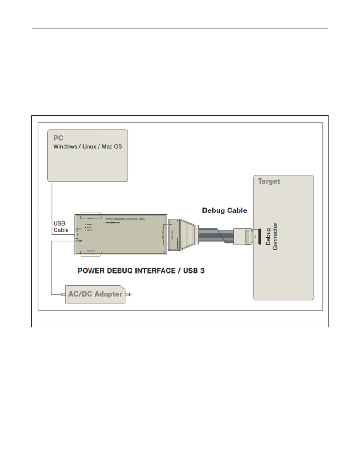
Figure 2 shows a generic JTAG setup using the Lauterbach probe.
Figure 2. JTAG Lauterbach setup diagram
The following is recommended:
• To prevent damage to the debuggers or target, do not plug or unplug the debugger while the target is powered on.
The recommended sequence for powering the debugger and target on or off is as follows:
• Power on: debugger > target
• Power off: target > debugger
— Make sure that the debugger connector orientation is correct when plugging it to the board to prevent damage to the
i.MX part.
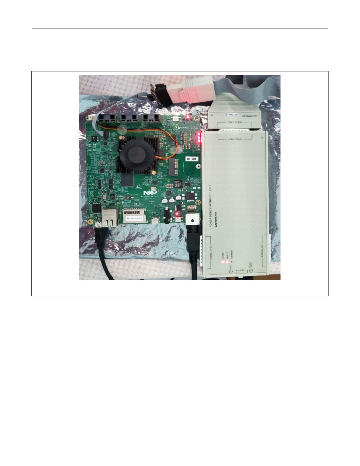
For example, see how the Lauterbach probe is connected to the i.MX8QXP MEK board in Figure 3.
1. Connect the Lauterbach JTAG debugger to the EVK board through the 10-pin JTAG interface.
Introduction to Boundary Scan of i.MX8/i.MX8X, Rev. 0, 04/2021
Application Note 3 / 11
Page 4
NXP Semiconductors
Hardware setup
2. Connect the Lauterbach JTAG debugger to the PC through the USB cable and then power on the debugger using a 5-V
power adapter.
3. Connect the MEK board to the power supply.
Figure 3. Lauterbach connected to i.MX8QXP MEK
5.1 Board setup for boundary scan
Each NXP SoC has the boundary scan conditions detailed in the hardware developer's guide document. The dedicated SoC BSDL
files describe the conditions to determine the SoC to enter the boundary scan mode.
For example, the i.MX8QXP BSDL file shows that the COMPLIANCE_PATTERNS needed for the boundary scan conditions are
as follows:
• Attribute COMPLIANCE_PATTERNS of MX8QXP: entity is "(TEST_MODE_SELECT, POR_B) (01)";
Under these conditions, the TEST_MODE signal must be set to low and the POR_B must be set to high. The boot selecting DIP
switches must be set to the "Serial Download Mode".
Introduction to Boundary Scan of i.MX8/i.MX8X, Rev. 0, 04/2021
Application Note 4 / 11
Page 5

NXP Semiconductors
Hardware setup
Figure 4. BOOT selection switches
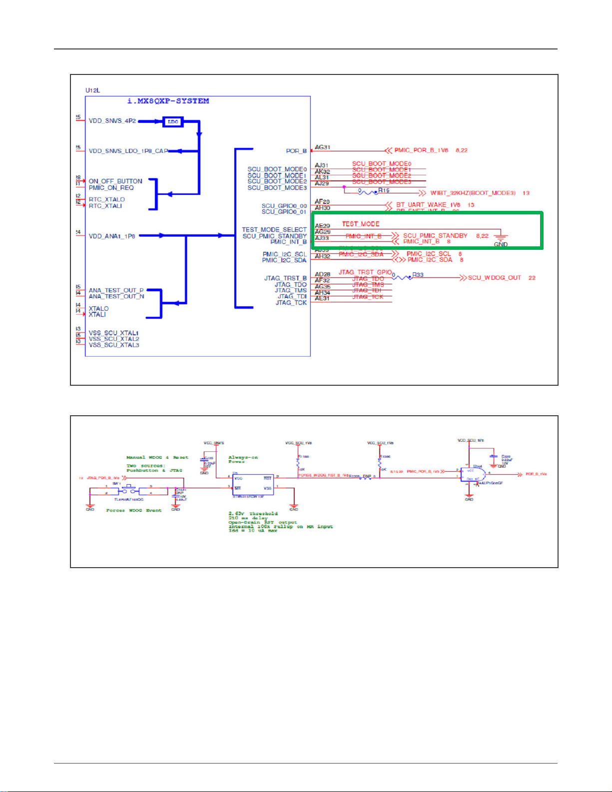
In the i.MX8QXP MEK board schematics, notice the following:
• The TEST_MODE signal is always low.
Introduction to Boundary Scan of i.MX8/i.MX8X, Rev. 0, 04/2021
Application Note 5 / 11
Page 6
NXP Semiconductors
Boundary scan using i.MX 8/i.MX 8 BSDL file and Lauterbach JTAG debugger
Figure 5. TEST_MODE signal always low
• The POR_B signal can be driven by the JTAG debugger/reset button to determine the BOOT ROM to enter the boundary
scan.
Figure 6. POR_B signal
6 Boundary scan using i.MX 8/i.MX 8 BSDL file and Lauterbach JTAG debugger
The recommendations before starting the boundary scan procedure are as follows:
• Using BSDL to check the board with an inappropriate multimeter can damage the board. Before performing
measurements, check what pins can be manipulated in the boundary scan safely without damaging the components
on your board.
• I/O pin power considerations: The boundary scan operation uses each of the available device pins to drive or read values
within a given system. Therefore, the power supply pin for each specific module must be powered for the IO buffers to
operate. This is straightforward for the digital pins within the system.
The boundary scan is as follows:
Introduction to Boundary Scan of i.MX8/i.MX8X, Rev. 0, 04/2021
Application Note 6 / 11
Page 7

NXP Semiconductors
Boundary scan using i.MX 8/i.MX 8 BSDL file and Lauterbach JTAG debugger
• Perform the software and hardware setups described in the previous sections. If the Lauterbach installation is properly
done, a “Trace32 Devices” entry appears in the Device Manager:
Figure 7. Trace32 Devices
• Open the TRACE32 software, type in the following commands with each command followed by the "Enter" key or create a
CMM script with the following commands:
— SYStem.Down
— BSDL.RESet
— BSDL.ParkState Select-DR-Scan
— BSDL.state
Figure 8. TRACE32 software
• The "BSDL.state" command opens a new window. Click the “FILE” button and load the BSDL file you want to validate.
Introduction to Boundary Scan of i.MX8/i.MX8X, Rev. 0, 04/2021
Application Note 7 / 11
Page 8

NXP Semiconductors
Figure 9. BSDL file
For the i.MX 8 SoC, four BSDL files are provided. Select the one that is compatible with the used i.MX 8QXP SOC
and has the power domain for ENET set according to the board schematics.
Boundary scan using i.MX 8/i.MX 8 BSDL file and Lauterbach JTAG debugger
NOTE
Figure 10. Board schematics
• After loading the file, type in the "BSDL.SOFTRESET" command followed by the "Enter" key.
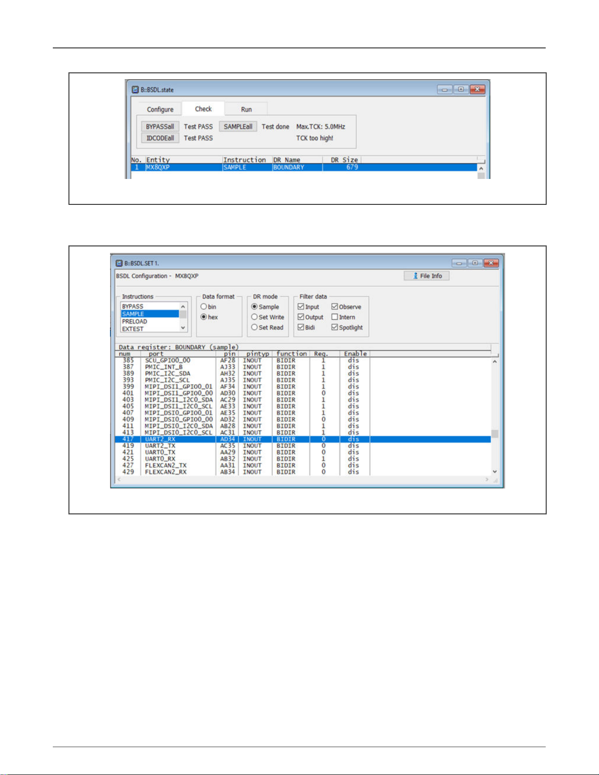
• Switch to the “Check” tab of the "BSDL.state" window. Click the “BYPASSall” and “IDCODEall” buttons to see if both
results can pass. The BYPASS/CLAMP/HIGHZ check passes.
Figure 11. BSDL.state window
• Click the “SAMPLEall” button and the “No result” entry changes to “Test done”. Then double-click the entity name and the
"BSDL.SET" window appears.
Introduction to Boundary Scan of i.MX8/i.MX8X, Rev. 0, 04/2021
Application Note 8 / 11
Page 9
NXP Semiconductors
Boundary scan using i.MX 8/i.MX 8 BSDL file and Lauterbach JTAG debugger
Figure 12. BSDL.SET window
• In the "BSDL.SET" window, uncheck the “Intern” checkbox to filter out the internal registers. The remaining contents is the
sampled value on each signal pin. Use a multimeter to measure the voltage of at least three signal pins and see if the
logic state matches the sampled value.
Figure 13. “Intern” checkbox
• Click the “EXTEST” entry in the “Instructions” list and choose the “Set Write” option in the “DR mode” field. Make sure
that the states of UART2_RX and UART2_TX are set to UART2_RX = output 1, UART2_TX = output 1 (if it exists). Then
switch to the "BSDL.state" window and check the “SetAndRun” and “TwoStepDR” checkboxes.
Introduction to Boundary Scan of i.MX8/i.MX8X, Rev. 0, 04/2021
Application Note 9 / 11
Page 10

NXP Semiconductors
Revision history
Figure 14. “SetAndRun” and “TwoStepDR” checkboxes
7 Revision history
Table 2. Revision history
Revision number Date Substantive changes
0 04/2021 Initial release
Introduction to Boundary Scan of i.MX8/i.MX8X, Rev. 0, 04/2021
Application Note 10 / 11
Page 11

How To Reach Us
Home Page:
nxp.com
Web Support:
nxp.com/support
Information in this document is provided solely to enable system and software implementers to use NXP products. There
are no express or implied copyright licenses granted hereunder to design or fabricate any integrated circuits based on the
information in this document. NXP reserves the right to make changes without further notice to any products herein.
NXP makes no warranty, representation, or guarantee regarding the suitability of its products for any particular purpose, nor
does NXP assume any liability arising out of the application or use of any product or circuit, and specifically disclaims any
and all liability, including without limitation consequential or incidental damages. “Typical” parameters that may be provided
in NXP data sheets and/or specifications can and do vary in different applications, and actual performance may vary over
time. All operating parameters, including “typicals,” must be validated for each customer application by customer's technical
experts. NXP does not convey any license under its patent rights nor the rights of others. NXP sells products pursuant to
standard terms and conditions of sale, which can be found at the following address: nxp.com/SalesTermsandConditions.
Right to make changes - NXP Semiconductors reserves the right to make changes to information published in this
document, including without limitation specifications and product descriptions, at any time and without notice. This
document supersedes and replaces all information supplied prior to the publication hereof.
Security — Customer understands that all NXP products may be subject to unidentified or documented vulnerabilities.
Customer is responsible for the design and operation of its applications and products throughout their lifecycles to reduce
the effect of these vulnerabilities on customer’s applications and products. Customer’s responsibility also extends to other
open and/or proprietary technologies supported by NXP products for use in customer’s applications. NXP accepts no
liability for any vulnerability. Customer should regularly check security updates from NXP and follow up appropriately.
Customer shall select products with security features that best meet rules, regulations, and standards of the intended
application and make the ultimate design decisions regarding its products and is solely responsible for compliance with all
legal, regulatory, and security related requirements concerning its products, regardless of any information or support that
may be provided by NXP. NXP has a Product Security Incident Response Team (PSIRT) (reachable at PSIRT@nxp.com)
that manages the investigation, reporting, and solution release to security vulnerabilities of NXP products.
NXP, the NXP logo, NXP SECURE CONNECTIONS FOR A SMARTER WORLD, COOLFLUX,EMBRACE, GREENCHIP,
HITAG, ICODE, JCOP, LIFE, VIBES, MIFARE, MIFARE CLASSIC, MIFARE DESFire, MIFARE PLUS, MIFARE FLEX,
MANTIS, MIFARE ULTRALIGHT, MIFARE4MOBILE, MIGLO, NTAG, ROADLINK, SMARTLX, SMARTMX, STARPLUG,
TOPFET, TRENCHMOS, UCODE, Freescale, the Freescale logo, AltiVec, CodeWarrior, ColdFire, ColdFire+, the Energy
Efficient Solutions logo, Kinetis, Layerscape, MagniV, mobileGT, PEG, PowerQUICC, Processor Expert, QorIQ, QorIQ
Qonverge, SafeAssure, the SafeAssure logo, StarCore, Symphony, VortiQa, Vybrid, Airfast, BeeKit, BeeStack, CoreNet,
Flexis, MXC, Platform in a Package, QUICC Engine, Tower, TurboLink, EdgeScale, EdgeLock, eIQ, and Immersive3D are
trademarks of NXP B.V. All other product or service names are the property of their respective owners. AMBA, Arm, Arm7,
Arm7TDMI, Arm9, Arm11, Artisan, big.LITTLE, Cordio, CoreLink, CoreSight, Cortex, DesignStart, DynamIQ, Jazelle,
Keil, Mali, Mbed, Mbed Enabled, NEON, POP, RealView, SecurCore, Socrates, Thumb, TrustZone, ULINK, ULINK2,
ULINK-ME, ULINK-PLUS, ULINKpro, μVision, Versatile are trademarks or registered trademarks of Arm Limited (or its
subsidiaries) in the US and/or elsewhere. The related technology may be protected by any or all of patents, copyrights,
designs and trade secrets. All rights reserved. Oracle and Java are registered trademarks of Oracle and/or its affiliates. The
Power Architecture and Power.org word marks and the Power and Power.org logos and related marks are trademarks and
service marks licensed by Power.org.
©
NXP B.V. 2021. All rights reserved.
For more information, please visit: http://www.nxp.com
For sales office addresses, please send an email to: salesaddresses@nxp.com
Date of release: 04/2021
Document identifier: AN13215
 Loading...