

Page 1

AN13202
EMC Design Recommendation on i.MXRT Series
Rev. 0 — 03/2021
1 Introduction
Electromagnetic Compatibility (EMC) plays an important role in the
contemporary product performance, so it is the prime reliability problem for
electronic equipment. Bad design may cause huge problems, so EMC is
valued at the first stage of a design. This document introduces how to make
EMC design reasonable based on i.MXRT series and helps users to maintain
robustness of the EMC performance in their products.
2 Overview
2.1 Basic knowledge of EMC theory
Electromagnetic interference is one of the major problems in modern electronic
systems. Designers need to pay attention on it at the early stages of the design
to prevent schedule delay issues caused by EMC problem.
To achieve electromagnetic compatibility, enough EMC knowledge and good
practice in EMC implementation are needed in all design phases.
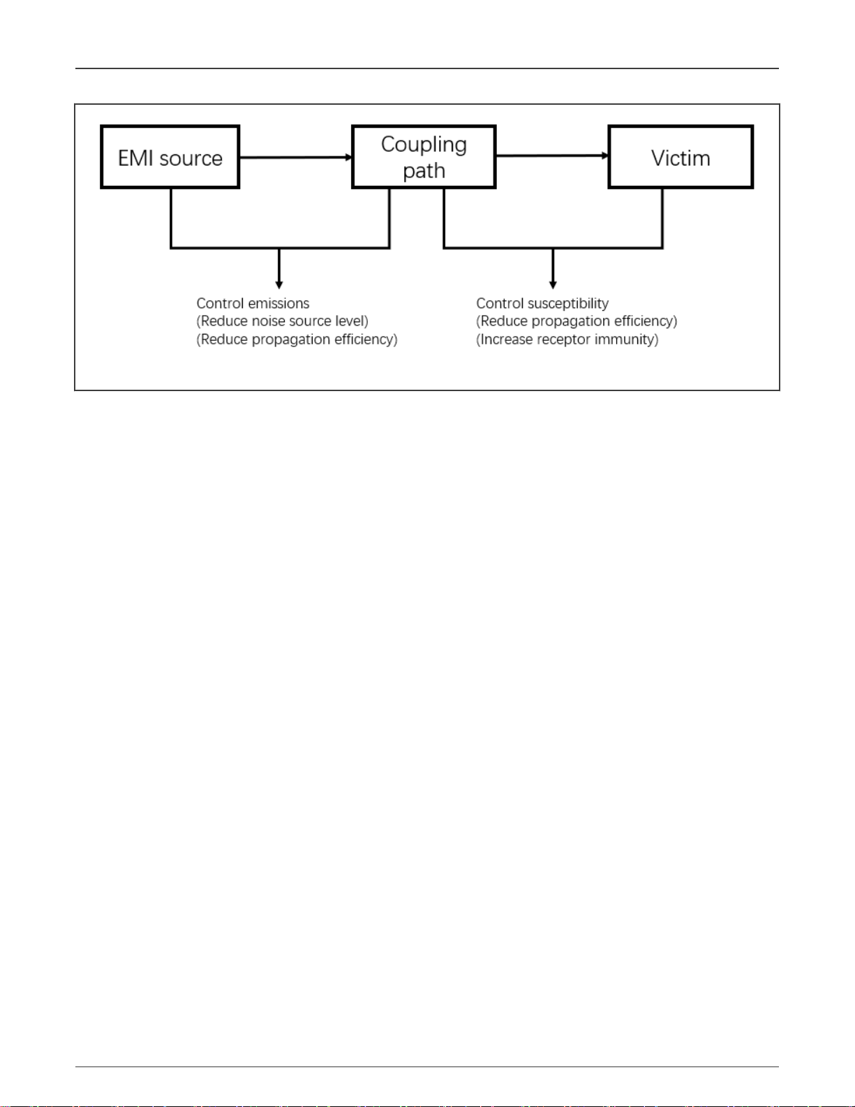
A simple EMI model consists of EMI source, coupling path and receptor, as
shown in Figure 1.
Application Note
Contents
1 Introduction......................................1
2 Overview......................................... 1
2.1 Basic knowledge of EMC theory
.....................................................1
2.2 Basic rules for EMC design..........2
3 Schematic design............................3
3.1 Crystal circuit............................... 3
3.2 Reset circuit................................. 3
3.3 Unused pins.................................4
3.4 Board-to-board interfaces............ 4
3.5 Communication interfaces........... 6
3.6 Sensitive signals impacted by
ground bounce.............................8
3.7 Power supply topology.................8
4 Layout design..................................9
4.1 Power supply routing and
grounding.....................................9
4.2 Placement..................................10
4.3 Bypass and decoupling..............11
4.4 DCDC circuit.............................. 11
4.5 Crystal oscillator circuit.............. 12
4.6 High speed signal...................... 12
4.7 Shield connection...................... 13
4.8 Isolation......................................14
4.9 Signal return path...................... 14
5 Software design............................ 15
5.1 Location of code running........... 15
5.2 Filter setting for some peripherals
...................................................15
5.3 IO drive strength........................ 16
5.4 Clock spread spectrum.............. 16
6 EMC test........................................18
6.1 Introduction................................ 18
6.2 EMC test results.........................19
7 Conclusion.....................................20
8 Reference......................................20
9 Revision history.............................20
Page 2
NXP Semiconductors
Overview
Figure 1. EMI elements
As shown in Figure 1, reducing noise from EMI source, altering coupling path and improving the immunity of the receptor can
eliminate the EMI issues in the system.
• Reducing noise from EMI source may include:
— Reducing loops area from the noise source
— Using of slower rising and falling edge repetition signal in noise source
— Reducing driving signal
— Adding filtering
— Shielding noise source circuitry
— Driving signal strength
— Filtering circuit
• Eliminating coupling path may include:
— Moving victim far away from the noise source
— Avoiding PCB traces coupling and power domains coupling between receptor and noise source
• Increasing immunity of victim may include:
— Reducing loops area from the PCB trace which is related to the victim
— Providing low impedance return path and reference power domains plane for signal traces related to the victim
2.2 Basic rules for EMC design
To better understand how to achieve the immunity (susceptibility) and emission requirements, some guidelines as below can help
designers to eliminate potential risks of redesigning system.
• There are different susceptibility requirements in electronic system but Radiated Immunity (RI) and Electrostatic Discharge
(ESD) test are basically same in modern electronic system.
• In RI test, the test system, EUT, will be exposed to high energy and very high frequency, so the circuit components,
in EUT, will be affected in some way. The basic design approach is to keep the sensitive component, microcontroller,
contamination out of the signal and power lines with predefined spectrum range (e.g. 10 - 900 MHz) .
• ESD generates short duration and high energy pluses (e.g. DC – 300 MHz) that will be introduced into EUT. It may cause
damage to some sensitive components in EUT. The basic design approach is to prevent sensitive circuit interfered by the
ESD high frequency components. Therefore, a system tends to provide high impedance with respect to chassis ground on
signal and power lines to eliminate the ESD current and energy input to the sensitive component.
EMC Design Recommendation on i.MXRT Series, Rev. 0, 03/2021
Application Note 2 / 21
Page 3

NXP Semiconductors
Schematic design
• For the emission, EUT provides assurance to a certain extent that it will not produce electromagnetic emissions to affect
other equipments. In general, many basic design techniques used in RI and ESD can be applied to solve emission issues.
The basic approach is to eliminate the high frequency interference voltage and current generation from EUT.
Some basic techniques, like component selection and PCB layout in
(document AN2321), can be applied to immunity and emission area mentioned above.
Designing for Board Level Electromagnetic Compatibility
3 Schematic design
The circuits listed below are more critical to affect EMC/EMI/ESD performance.
• Crystal circuit
• Reset circuit
• Unused pins disposition
• Interface of board to board
• Communication interface
• Power topology
This chapter introduces the detailed design aspects. It takes a concentrator board using i.MX RT1060 processor as an example
to introduce the design rules related to these aspects.
3.1 Crystal circuit
For i.MXRT series, an external 24 MHz crystal is required for the primary clock reference. The reference clocks with external clock
sources, such as active oscillators, are acceptable. An external oscillator has better ESD performance than a crystal. According
to our experiments, the performance of the systems using oscillator as a reference, compared to using crystal, improves about 2
KV ESD.
Using internal clock as reference clock can improve EMC performance, but for RT10XX series, internal clock doesn't support to
be PLL reference clock, and any other part that supports this feature will be taken as an EMC improvement.
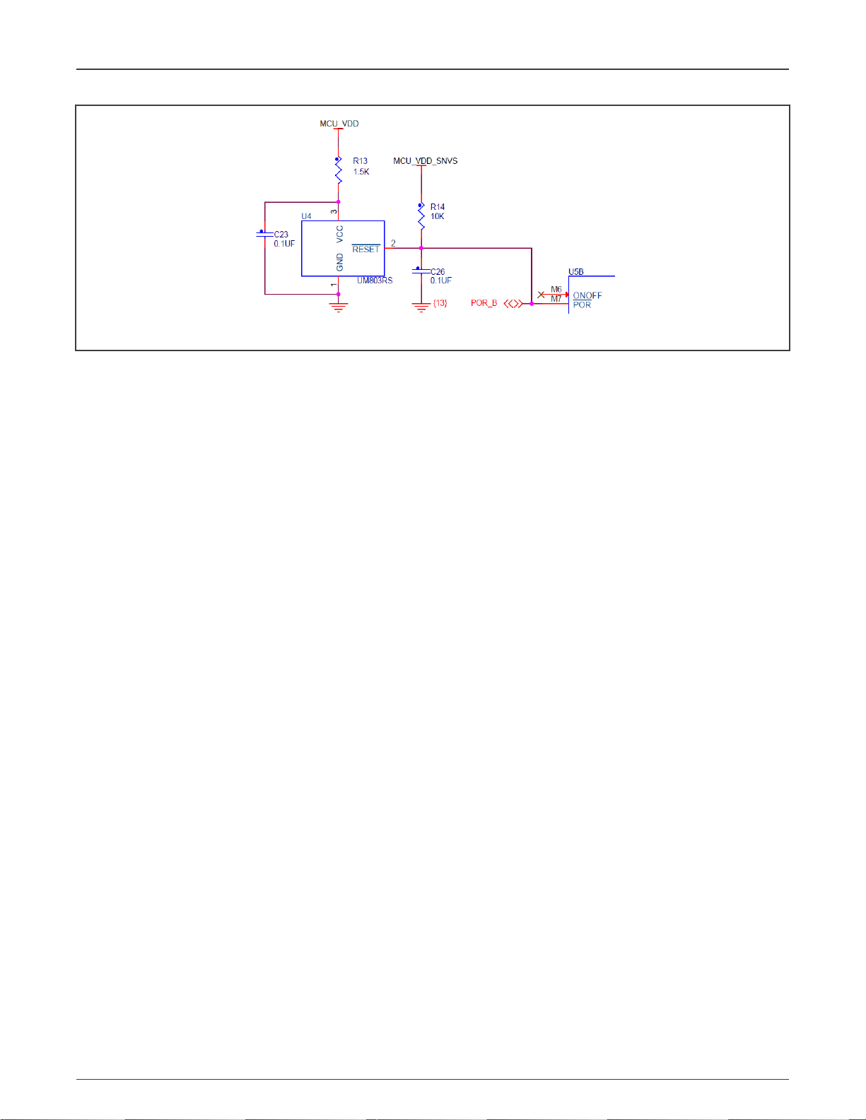
3.2 Reset circuit
The chip has a System Reset Controller (SRC) managing the various reset signals. The external reset signal is routed to SRC via
a reset pin named POR_B.
A voltage supervisor IC is recommend to control POR_B. It provides reliable reset signal and monitors the power supply for low
voltage detection, which can help to avoid the potential EMC issue.
To avoid the noise Interference in poor EMC condition, place a RC circuit close to POR_B pins, which can decouple noise and
improve EMC performance.
Figure 2 shows one POR circuit as reference.
EMC Design Recommendation on i.MXRT Series, Rev. 0, 03/2021
Application Note 3 / 21
Page 4
NXP Semiconductors
Figure 2. Chip POR circuit
As the POR_B is driven by multiple sources, either of the below is required:
1. The output of the supervisor IC is open-drain output type.
2. An inverse diode connected into the supervisor IC’s output if it has a push-pull output.
POR_B is in SNVS power domain of the processor, so it needs to be pulled up to the power supply of SNVS.
Schematic design
3.3 Unused pins
Unused pins possibly impact EMC performance. They probably increase power consumption and the related GPIO status may
be changed under poor EMC conditions. For instance, a pin with High-Z impedance input, under poor EMC conditions, probably
frequently switches status, which increases the power consumption and causes other EMC issues.
Do not connect unused pins directly to GND, as the GPIO configuration registers may be changed under poor EMC conditions.
If the output is high in this case, big current will be generated and the pin may be damaged.
Generally, the datasheet provides the recommendations for unused pins connections. Follow the below rules:
• Refer to the datasheet to determine whether the unused pins are allowed to be floating or not.
• If a pin is allowed to be floating, configure it as GPIO and outputs 0 or 1.
• If a pin isn’t allowed to be floating, it is suggested to pull-down to GND with a resistor like 10 kΩ.
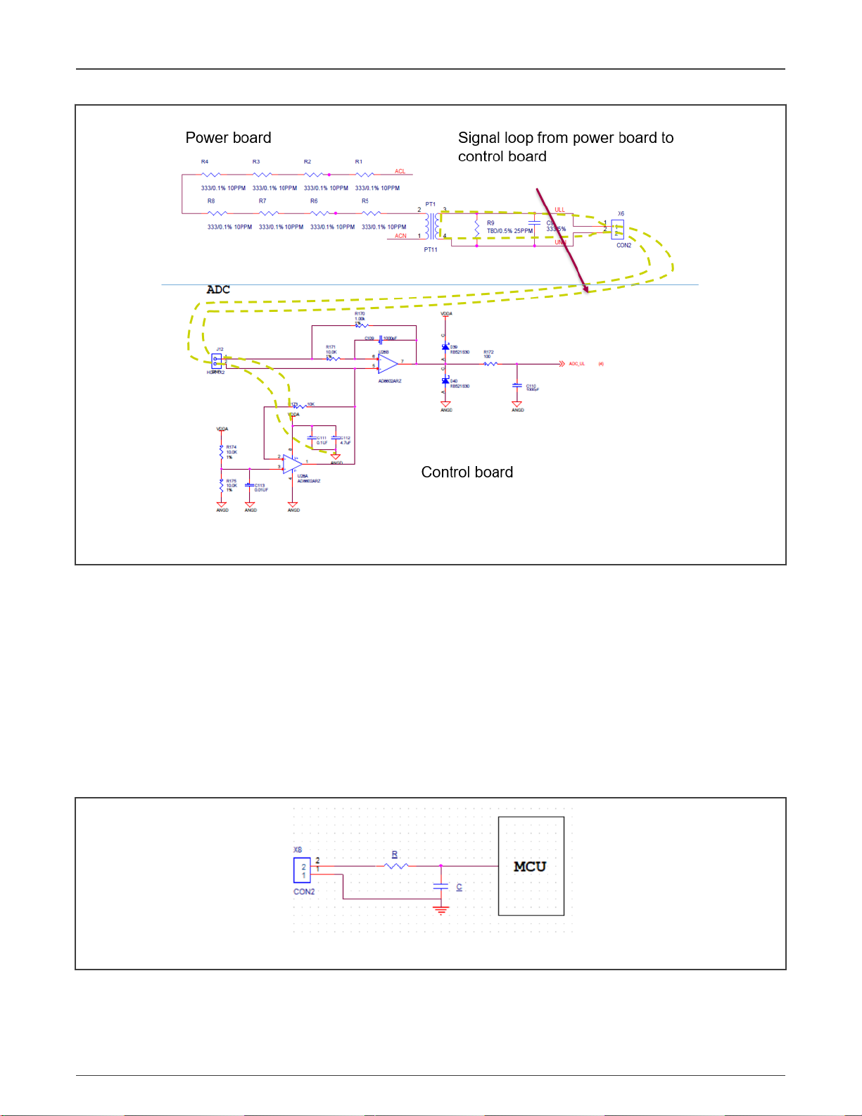
3.4 Board-to-board interfaces
Check signal loop for some signals being across board-to-board connection. Big signal/power loop possibly gets the poor EMC
performance and gets EMC issue. Figure 3 shows a bad example.
EMC Design Recommendation on i.MXRT Series, Rev. 0, 03/2021
Application Note 4 / 21
Page 5
NXP Semiconductors
Schematic design
Figure 3. Example of board to board connection
The system has two boards, the power board and the processor control board. The AC signal is from the power board to the
processor control board, so the signal loop with high impedance from VDDA through operational amplifier(U28)to AGND is so
long. It will couple more noise and input into the processor.
There are two solutions to shorten signal loops in the design shown in Figure 3.
1. Move PT1 to the processor control board, and input signal loop of amplifying is shortened a lot. The EMC performance
with Direct Contact Discharge is improved from from 4 KV to 8 KV.
2. Move the operational amplifier circuit to the power board and connect VDDA and AGND to the power board. It gets a
small loop among the ADC signal, VDDA, and AGND, to improve EMC performance.
For a processor IO directly connecting to a connector, introduce a TVS component as ESD protection. Another low-cost solution is
to add RC components as shown in Figure 4. For the R/C values, consider the IO operating frequency and set the RC time constant
far less than the signal period.
Figure 4. Example of IO interface
If there are high-speed signals or clock signals in board-to-board interface, it possibly gets EMI issue due to long signal loop and
big harmonic energy. To reduce the signal loop and harmonic energy, place the GND signals close to high-speed signals and
EMC Design Recommendation on i.MXRT Series, Rev. 0, 03/2021
Application Note 5 / 21
Page 6

NXP Semiconductors
Schematic design
reserve the serial resistor on board. If the signals support to change drive strength by software, lower drive strength to reduce
harmonic energy.
3.5 Communication interfaces
Regarding the communication interfaces, take below actions to improve the EMI and ESD performance.
• Connect TVS diodes for all signals from/to the connectors for transient voltage suppression.
• Connect a ferrite bead between power supplies of connectors and the power supplies of the board to isolate high
frequency noise.
• Connect a common mode choke between a pair of differential signals to remove high frequency common mode noise.
• Connect parallel RC or ferrite bead components between the connector’s metal shield and the board GND.
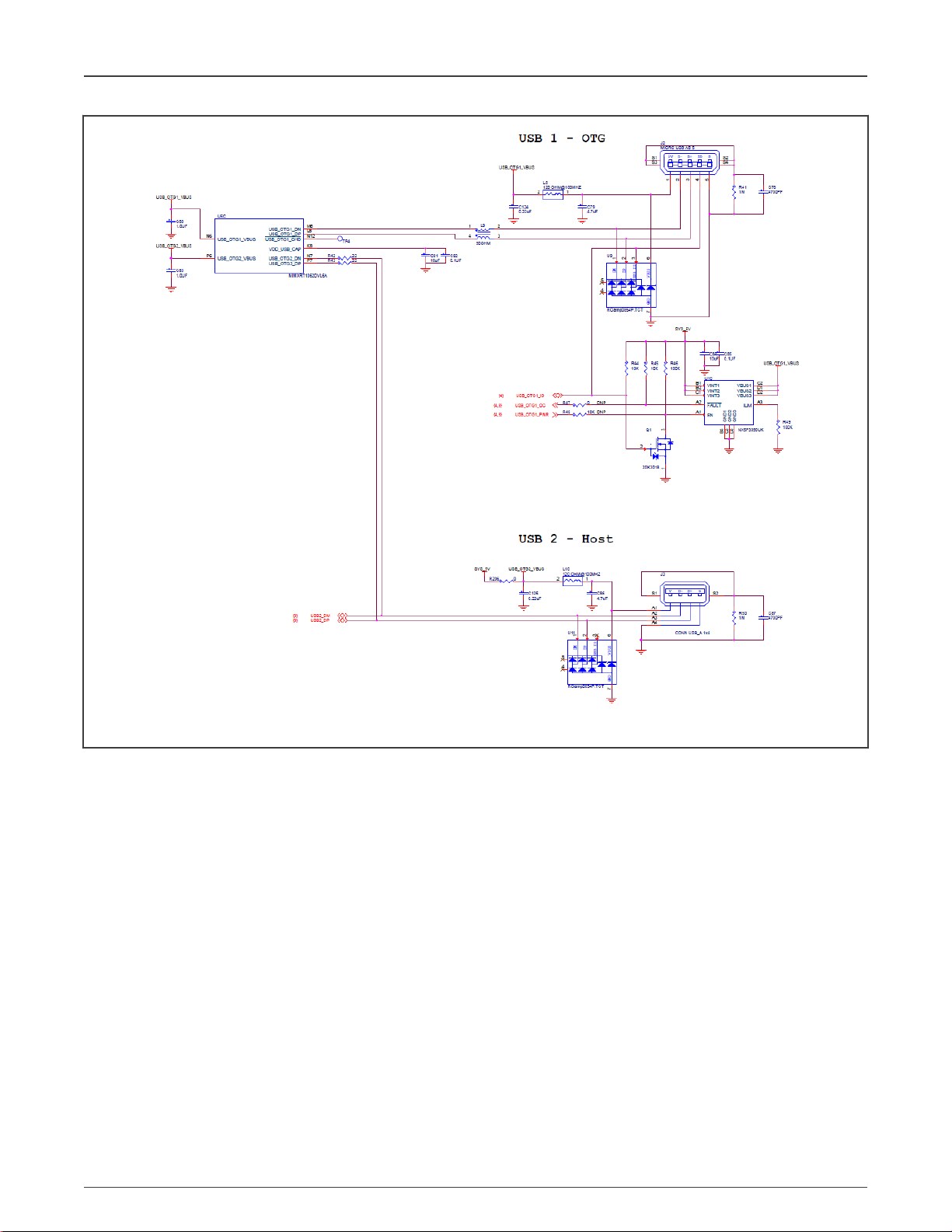
3.5.1 USB
Take below solutions to improve EMC performance.
• TVS arrays is recommended for ESD protection on VBUS, D+, D-, and ID.
• To improve EMI performance, connect the common mode choke to USB signal.
• Ferrite beads on power pin (VBUS,GND) are introduced to isolate high frequency noise.
• To improve ESD performance, take RC or Ferrite bead to isolate USB shield and board GND.
Figure 5 is an example circuit used in i.MXRT1060 concentrator board.
EMC Design Recommendation on i.MXRT Series, Rev. 0, 03/2021
Application Note 6 / 21
Page 7
NXP Semiconductors
Schematic design
Figure 5. USB circuit
3.5.2 Ethernet
For Ethernet design, a recommend design from EMC view as below:
• Use the TVS arrays for ESD protection on signals TXP, TXN, RXP, and RXN.
• Use the ferrite bead to isolate high frequency noise from the transformer.
• To improve ESD performance, use RC or Ferrite bead to isolate Ethernet shield and board GND.
Figure 6 is an example circuit used in i.MXRT1060 concentrator board.
EMC Design Recommendation on i.MXRT Series, Rev. 0, 03/2021
Application Note 7 / 21
Page 8

NXP Semiconductors
Schematic design
Figure 6. Ethernet circuit
3.5.3 JTAG
JTAG is the popular interface for debug during developing phase. It is sensitive and easy to get issues under the condition of poor
electrical magnetic environment. Reserve the serial 0ohm resistor on JTAG signals during developing phase and remove 0ohm
resistors to disconnect JTAG signals on production.
3.6 Sensitive signals impacted by ground bounce
i.MXRT series contains multiple power domains, like SEMC, SD0, SD1, NVCC_GPIO, and so on. i.MXRT series supports multiple
parallel protocol interface, like SDRAM, LCD, CSI. These parallel interfaces work and multiple IOs change logic status from 1 to
0 or from 0 to 1 at the same time, to get the parasitic capacitor and inductance charge and discharge frequently. It creates the
ringing on the ground plane and DC supply rail. This situation possibly impacts some sensitive signals, especially those that have
the same power domain with these parallel interfaces.
For example, the General Purpose Timer (GPT) module supports capture feature. Two GPT capture pins remap to GPIO_EMC_40
and GPIO_EMC_41, whose edge is sensitive for capture function. It possibly gets false trigger if ground issue occurs due to SDRAM
working, because pins of GPIO_EMC_00 to GPIO_EMC_39 are in the same power domain and get big impact.
To avoid this issue, follow suggestions as below:
1. To avoid or reduce ground bounce, follow the layout suggestion of high speed signals shown in Layout design.
2. Do not assign the sensitive signals to the same power domain with parallel interface.
3. To avoid or reduce ground bounce, add external RC circuit to sensitive signals.
3.7 Power supply topology
Plan the power topology at the beginning of design, including power components selection, voltage for each power rail, power
sequence and so on. should be considered firstly. The power diagram for schematic design can give a clear picture of whole
power supply.
EMC Design Recommendation on i.MXRT Series, Rev. 0, 03/2021
Application Note 8 / 21
Page 9

NXP Semiconductors
Layout design
Table 1 takes i.MXRT1060 concentrator board as example to summarizes the power domains of these reference design in details.
Table 1. Power domains of concentrator board
Power domain name Default voltage
(V)
SYS_5V
RS485_5V
SYS_3V3
MCU_VDD
VDDA
MCU_VDD_SNVS
DCDC_OUT
5 • Supplied from jack, or the ACDC board, or the USB OTG/device VBUS.
5
3.3
3.3
3.3
3.3
1.0
Descriptions
• Powering the DCDC convertor and USB host
• Supplied by the ACDC board.
• Powering RS485 interface.
• Generated from the DCDC convertor.
• Powering supply for the processor and most of the on board components.
• Derived from SYS_3V3.
• Powering main power of the processor, such as, DCDC_IN, VDD_HIGH_IN,
VDDA, and various IO domains.
• Derived from MCU_VDD.
• Powering processor VDDA_ADC_3P3 and on-board analog components.
• Generated from an LDO or battery.
• Powering processor VDD_SNVS_IN.
• Output of the internal DCDC convertor.
• Powering VDD_SOC_IN.
VDD_SOC_IN
USB_OTG1_VBUS
USB_OTG2_VBUS
1.0
5.0
5.0
• Derived from DCDC_OUT for the processor core domain.
• VBUS of USB_OTG1.
• VBUS of USB_OTG1.
• Generated from an LDO which powered by SYS_5V.
VDD_GPRS
4.0
• Powering external GPRS module.
4 Layout design
4.1 Power supply routing and grounding
4.1.1 PCB stack-up
There are high speed signal interfaces in i.MXRT series design, such as SEMC, Octal SPI and LCD, so a PCB layout with at least
4-layer stack-up design is strongly recommended.
The below lists some advantages of the 4-layer stack-up design:
• There will be ground and power plane well used as reference in controlled impedance line for high speed and differential
signals.
EMC Design Recommendation on i.MXRT Series, Rev. 0, 03/2021
Application Note 9 / 21
Page 10
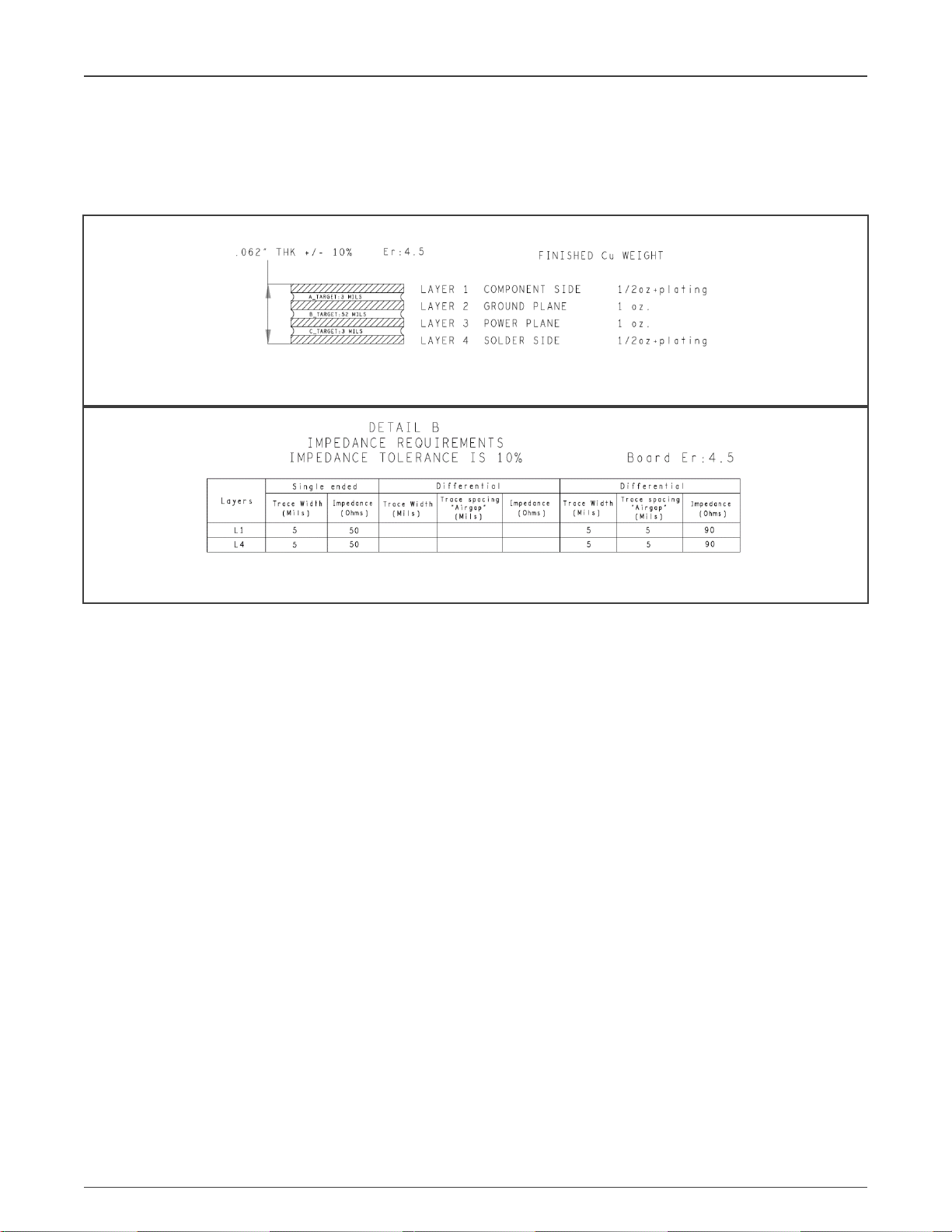
NXP Semiconductors
Layout design
• The ground and power plane provides a shorter signal current return loop, and reduce the ground-power impedance.
• The larger current return loop is directly related to a larger loop antenna and the size of antenna directly affects the
generation of noise. Shortening the antenna can avoid the EMI interference and improve the EMC performance efficiently.
Figure 7 shows an example for 4-layer stack-up design.
Figure 7. PCB stack-up
Figure 8. Impedance control in signal layer
4.1.2 Power and ground plane
In multi-layer board layout design, to reduce the impedance of power and ground plane, assign the independent power and
ground plane.
• 20-H rule is the guideline for multi-layers board design with power and ground plane. The rule suggests the ground plane
should be expanded beyond the power plane by 20 times the distance between the two plane. That is for reducing the
influence of fringing field radiation at the edges of the board.
• Place more ground vias on a complete, continuous and solid plane for power and ground.
• Enlarge the plane area and place the connecting vias at a suitable position. It could make the power and ground plane in
lower impedance, which can help to provide a low impedance return loop for signal return current.
• Avoid across reference planes when doing signal trace routing.
4.2 Placement
When placing components in PCB layout, pay attention to the below points. Before doing the component placement, sort the
different function circuit, such as power supply, analog circuit, digital circuit and high speed interface connector. These circuits
should be placed to different area of PCB board.
• Place the power supply circuit together with the board power supply input. Place the component from high voltage to low
voltage circuit.
• Place the decoupling capacitors of DC/DC or LDO voltage regulator as close as possible to the input and output port.
• Compared with digital circuit, the analog circuit is more sensitive. Place the analog circuit away from high voltage and high
speed digital circuit, which can reduce the coupling path of noise.
• Keep enough clearance between high speed interface connector and sensitive component.
• Pay more attention to RF, AD/DA and analog sensor circuit, as they are more sensitive to noise.
EMC Design Recommendation on i.MXRT Series, Rev. 0, 03/2021
Application Note 10 / 21
Page 11
NXP Semiconductors
Layout design
• Place the crystal as close as possible and surround with ground plane. Keep safety distance from other sensitive
component.
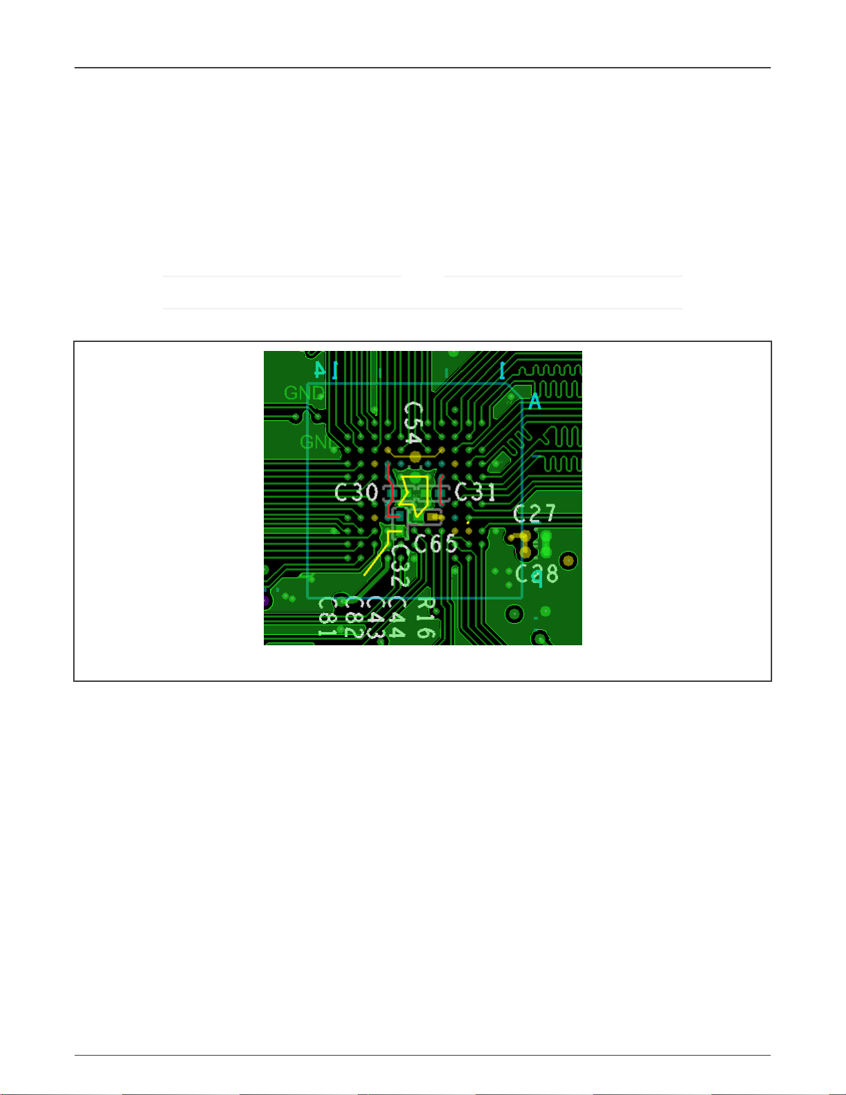
4.3 Bypass and decoupling
Place the small decoupling capacitors and the larger bulk capacitors close to MCU power pin. Get current first pass through
capacitor and then go to power pin.
For BGA package, place the decoupling capacitors and the bulk capacitors as close as possible to the power balls. It is critical to
minimize parasitic inductance and maintain high-speed transient current as the demand of the processor.
NOTE
For the current return path of decoupling and bypass capacitors, keep the return path as short as possible.
See Figure 9 for decoupling capacitor routing.
Figure 9. Decoupling and bypass capacitors placement and return current loop
4.4 DCDC circuit
The internal DC/DC of i.MXRT family contains one or two outputs for the core platform supply and its switching frequency is about
1.5 MHz.
The DC/DC requires external inductor and capacitors. See the hardware design guide for the external inductor and capacitors
component selection.
To keep good EMC performance, the below items are critical for the layout of DCDC circuit.
• Keep the DC/DC current loop as small as possible to avoid EMI issues.
• Enable current first pass through filter capacitors and then go to pins.
• Avoid unnecessary via between inductor and bulk capacitors.
See Figure 10 for reference to trace route out from RT1062 DCDC_LP. Directly route to L7 (4.7uH) inductor without any via and
then current pass through C41 and C42. Directly connect the ground of C41 and C42 to RT1062 DCDC GND, which gets short
return path with small impedance.
EMC Design Recommendation on i.MXRT Series, Rev. 0, 03/2021
Application Note 11 / 21
Page 12

NXP Semiconductors
Figure 10. DCDC layout on i.MXRT1062
Layout design
4.5 Crystal oscillator circuit
There are two kinds of crystal oscillator circuit on PCB board: crystal and external oscillator. The crystal is connected between
XTALIN and XTALOUT of MCU pins. The crystal/oscillator is the source of noise and also a sensitive victim. So it should be well
protected and routed carefully. Some experienced routing methods are strongly recommended.
• The route trace between crystal and XTALIN/XTALOUT should as short as possible. Also keep the length of the two
traces equivalent.
• Place the load capacitors and feedback resistors near the crystal to reduce the influence of parasitic parameters.
• Keep isolation with GROUND between crystal and other circuit components.
• Keep a solid GND plane directly under the crystal-associated components and trace.
• Do not route signal traces across the area under the crystal and under-plane.
• Improve the drive strength of oscillator will get better EMS performance, but possibly increase power consumption and
EMI influence.
• External oscillator may have better EMS performance than crystal.
4.6 High speed signal
The following list provides recommendations for routing the traces of high-speed signals.
NOTE
To well communicate with the devices, consider the propagation delay and the impedance control.
• The high-speed signals (SDRAM, RMII, RGMII, USB, Display, Hyper flash, SD card) must not cross gaps in the reference
plane.
• Avoid creating slots, voids, and splits in the reference planes.
• Provide ground return vias within a 100-mil from the signal layer-transition vias when transitioning must between different
reference ground planes.
• The clocks or strobes that are on the same layer need at least 2.5 times spacing from the adjacent traces (2.5 times
height from the reference plane) to reduce crosstalk.
EMC Design Recommendation on i.MXRT Series, Rev. 0, 03/2021
Application Note 12 / 21
Page 13
NXP Semiconductors
Layout design
• Match the data, address, clock, and CMD trace lengths (length delta depends on the bus rates), and ensure to keep the
same via number.
Figure 11 shows example for SDRAM routing.
Figure 11. High speed signal trace between RT1060 MCU and SDRAM
4.7 Shield connection
Some jacks are metal or with a conductive housing, reveal out of case or touchable, design consideration with ESD immunity is
very important, for example, USB and Ethernet jack, some basic design rules as below:
• Place a separate shield (ethernet/USB) chassis ground under the jack.
• Connect the chassis ground to the rest of the PCB GND with RC or ferrite beads. The location and value selection is
critical to EMC and EMI performance.
• Keep chassis ground return loop as small as possible and avoid to across key signals or components, such as,
microcontroller.
Figure 12 shows an example.
Figure 12. Shield connection example
EMC Design Recommendation on i.MXRT Series, Rev. 0, 03/2021
Application Note 13 / 21
Page 14
NXP Semiconductors
Layout design
Instead of directly connecting to the board digital GND, route shield GND passing through RC circuit or ferrite bead to power supply
GND. To prevent noise interference from digital GND, protect sensitive signals.
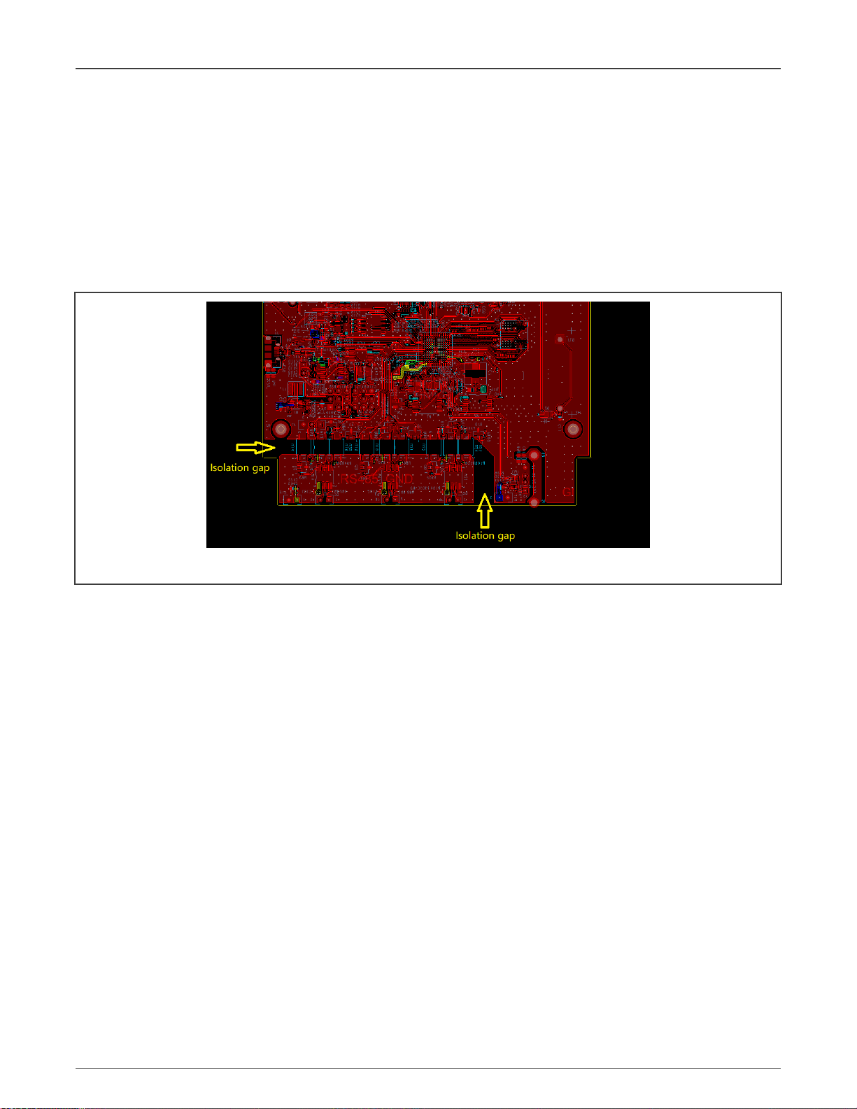
4.8 Isolation
Isolation is frequently used in design, for example, isolate strong power and weak power, or different power domain. This
document takes RS485 circuit used in i.MXRT1060 concentrator board as an example to introduce layout consideration.
An optical isolator IC is used to isolate RS485 receiver and system MCU IO. To improve the isolation performance, employ the
isolation gap under the RS485 receiver, in all planes (Top/Power/GND/Bottom).
Figure 13 shows an example for RS485 with isolation circuit.
Figure 13. RS485 IO isolation gap
4.9 Signal return path
An electrical circuit has a close loop between source and terminal device. Up to now, the signal return loop is discussed more
frequently than power one. In fact, both the signal and power have their own current return loop. The ground plane can be the
reference plane for signal and power, and the power plane can also be the reference plane for signal. The smaller area and
impedance of return loop is, the less impact of cross talk and Electromagnetic Interference (EMI). Figure 14 shows a DC-DC
regulator circuit. The decoupling capacitors are placed close to the input/output port and the return current can loop back from top
layer to minimize the return current loop and impedance.
EMC Design Recommendation on i.MXRT Series, Rev. 0, 03/2021
Application Note 14 / 21
Page 15

NXP Semiconductors
Figure 14. DC-DC current return loop path
Software design
Considering the signal return path, avoid the slot on current return loop path. Remember that the smaller area for the current return
loop leads to the better performance for EMC design.
5 Software design
Software is a good solution to improve EMC performance. Software can improve the system robustness with no extra cost added.
For details, see below points on i.MXRT series.
5.1 Location of code running
i.MXRT series support to execute code in:
• XIP flash, such as, QSPI flash interface with FlexSPI module
• Internal SRAM
• External RAM, such as, SDRAM
It can get better performance in internal SRAM compared to external SRAM and XIP flash.
Code is easily interfered by noise when running in external memory. To improve performance, put code into internal SRAM.
5.2 Filter setting for some peripherals
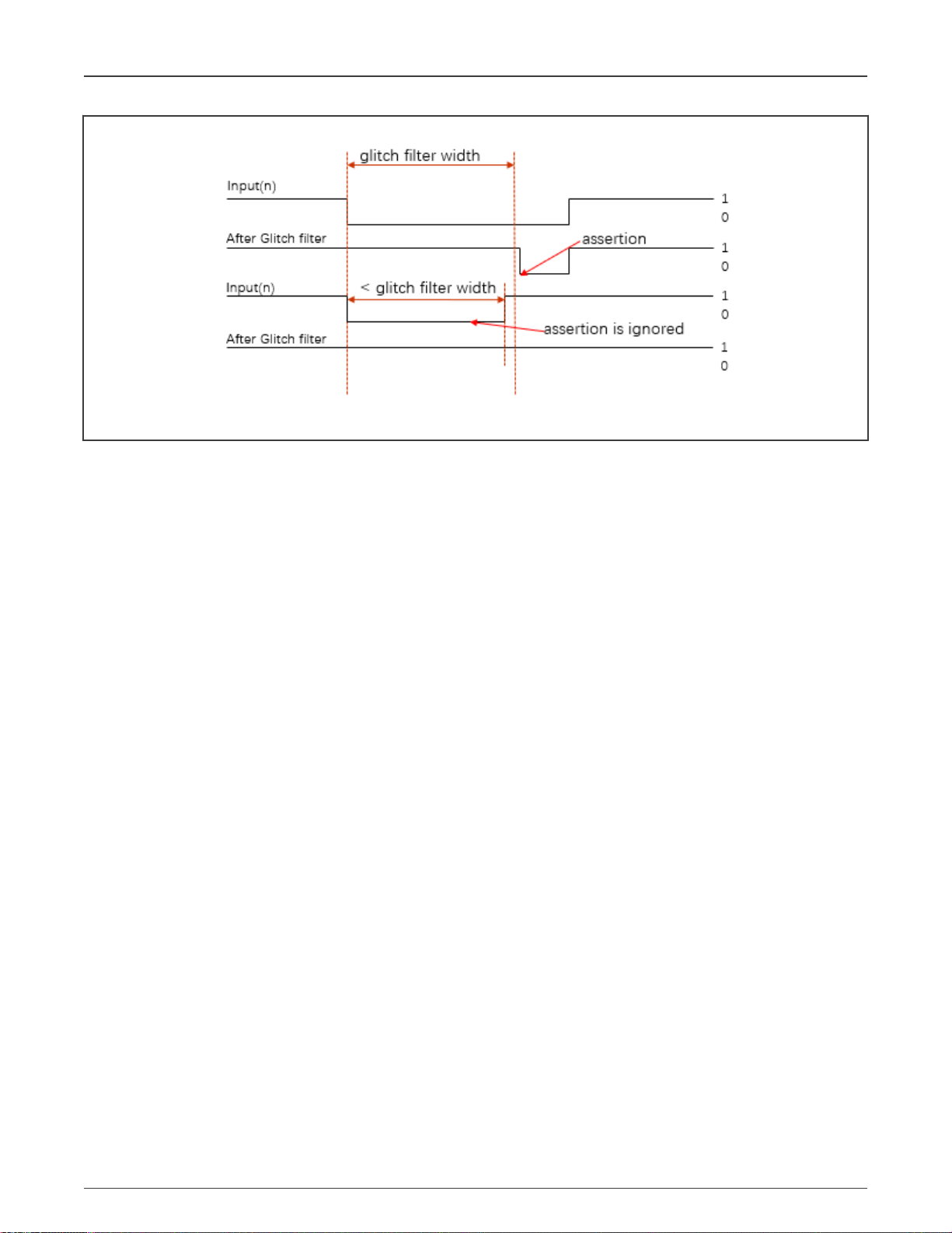
Some peripherals support digital filter to avoid noise interference, such as LPI2C, FlexCAN,ENC and tamper pins in i.MXRT
series. This feature can filter the noise input with specified periods. Figure 15 shows the digital filter.
EMC Design Recommendation on i.MXRT Series, Rev. 0, 03/2021
Application Note 15 / 21
Page 16
NXP Semiconductors
Software design
Figure 15. Digital filter working
As shown in Figure 15, noise can be filtered out by configuring the glitch filter width according to application. To improve EMC
performance, enable the filter configuration.
Taking i.MXRT1060 concentrator board as an example, it fails during the EFT test with 4 KV level. LPI2C fails to work during EFT
test. After LPI2C glitch filter is enabled, it can pass EFT test with 4.5 KV level.
5.3 IO drive strength
Generally, Electromagnetic Interference (EMI) issue can be caused by high speed clock or fast IO switching. For the I/O, especially
the high speed interface, fast I/O switching contains many high frequency harmonic energy, which easily produces EMI issue.
To reduce harmonic impact, cascaded one right resistor to slow down the edge of I/O and reduce overshot and undershot.
Fortunately, i.MXRT series provide the capacity to configure IO drive strength by the software. Software solution can get similar
results, which can save cost and is easy to use.
When the production gets the EMI issue, try to find out interference source by analysis harmonic and try to reduce the related I/O
drive strength, which can help to solve EMI issue.
For example, on the RT1060 EMC concentrator board, more harmonic at multiple of 50 MHz and analysis system are found and
ENET REF_CLK is 50 Mhz. After changing the ENET REF_CLK pad setting from 0x31 to 0x21 to lower the drive strength, noise at
multiple of 50 MHz can be reduced.
5.4 Clock spread spectrum
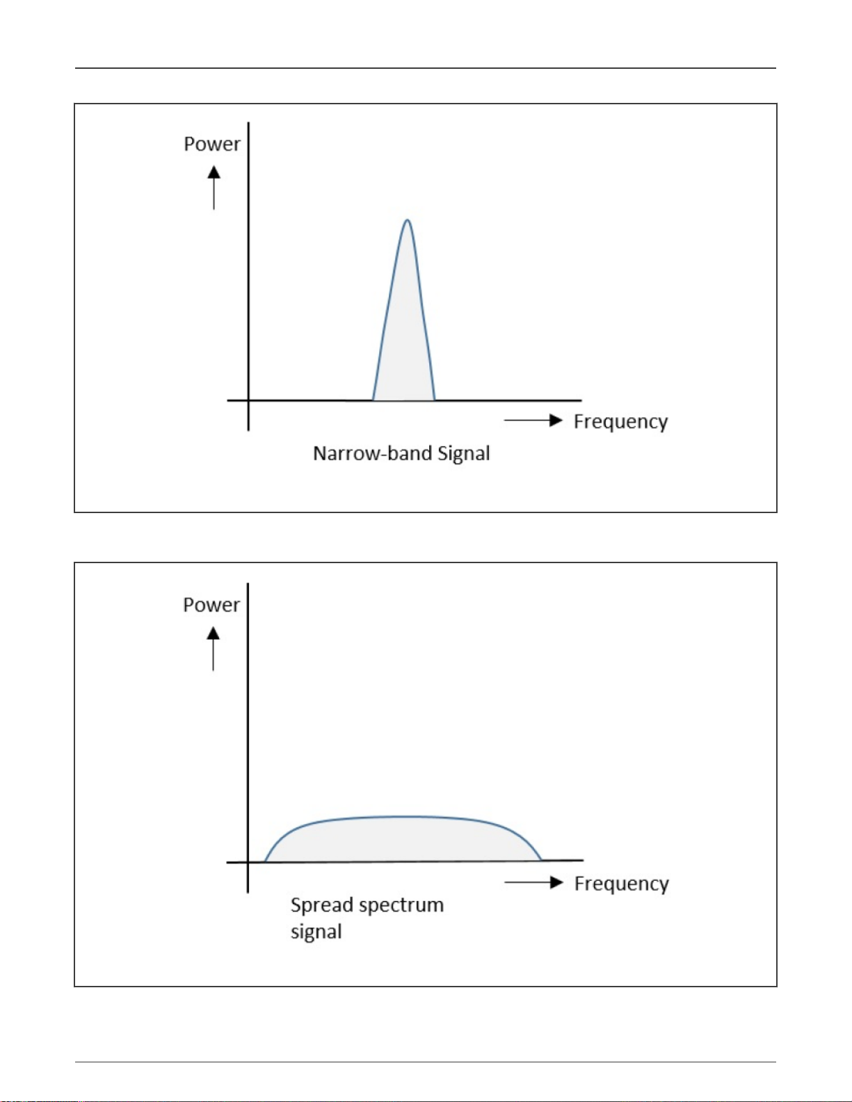
System PLL is a clock source for internal system buses, internal processing logic, SDRAM interface, and NAND/NOR interface
modules, etc. The system PLL and these peripheral working frequency are very high, which is the main source to create
electromagnetic emission. Figure 16 shows the narrow-band signals and signal strength to be concentrated.
EMC Design Recommendation on i.MXRT Series, Rev. 0, 03/2021
Application Note 16 / 21
Page 17
NXP Semiconductors
Software design
Figure 16. Narrow-band signals
To reduce signal concentrated, a spread-spectrum technique is introduced. It gets the energy of the clock within a certain
bandwidth to be dispersion and the peak amplitude of the electromagnetic energy level is reduced, as shown in Figure 17.
Figure 17. Spread spectrum signals
EMC Design Recommendation on i.MXRT Series, Rev. 0, 03/2021
Application Note 17 / 21
Page 18
NXP Semiconductors
EMC test
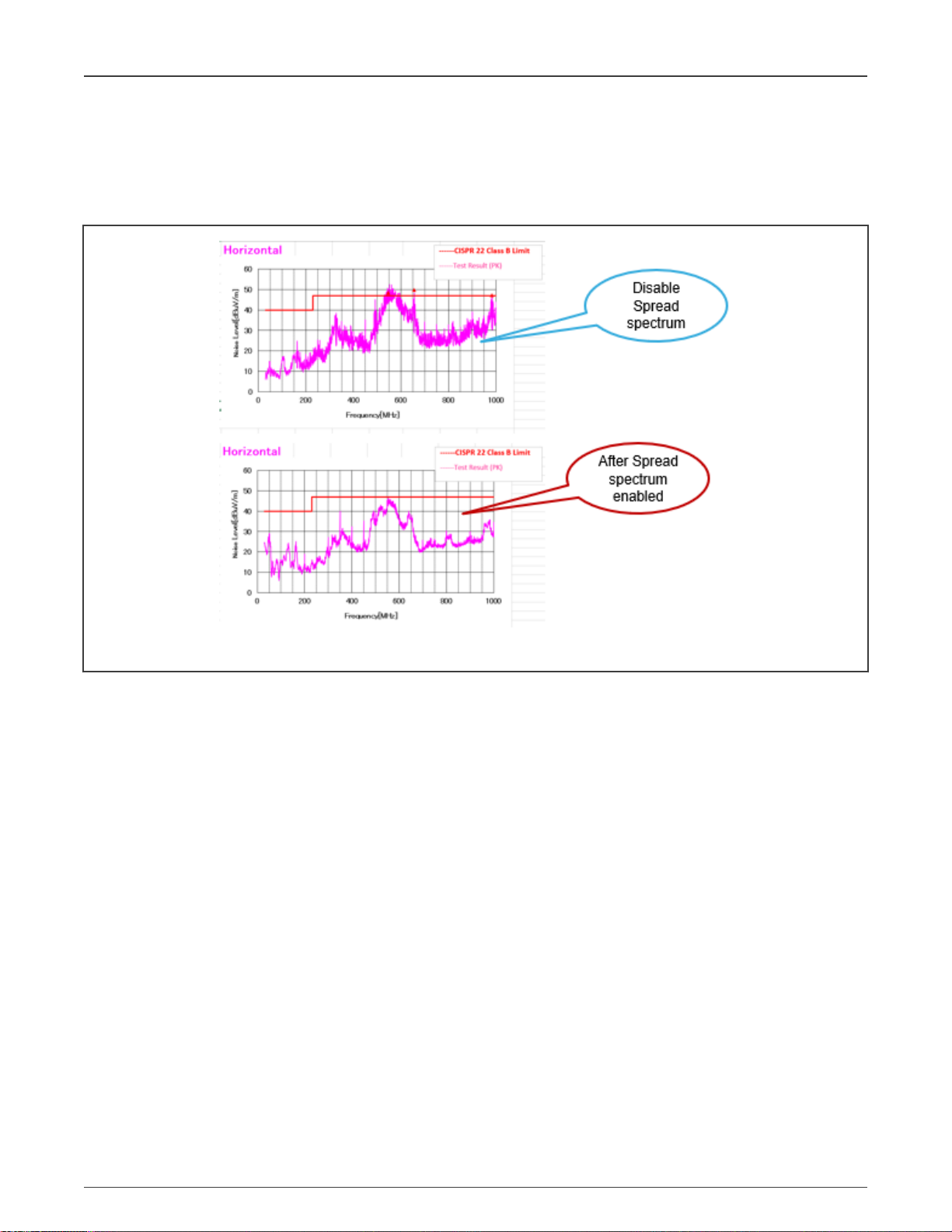
The System PLL i.MXRT series offers the spread spectrum supported. If peripherals take this PLL as clock source, enable this
feature to reduce EMI impact. For detailed information on how to enable this feature, see
Family
(document AN12879).
In RT1060 concentrator board, after enabling spread spectrum feature on system PLL, it improves by about 5 dbm, as shown in
Figure 18.
How to Enable Spread Spectrum for RT
Figure 18. Comparison of spread spectrum function
6 EMC test
Taking MIMXRT1062 concentrator board as an example, evaluate the RT1062 board-level and system-level EMC performance
based on IEC61000-4-2 and IEC61000-4-4 standards.
6.1 Introduction
Figure 19 shows the block diagram of concentrator board based on RT1060.
EMC Design Recommendation on i.MXRT Series, Rev. 0, 03/2021
Application Note 18 / 21
Page 19

NXP Semiconductors
Figure 19. Block diagram of concentrate board
EMC test
The below functions are supported during the test:
• 4-layer board
• AC220 input, taking AC-DC power board as the DC supply for the concentrator board
• i.MXRT1062 running in 600 Mhz
• QSPI flash working in 133 Mhz, SDRAM working in 166 Mhz
• Periodically send/receive data and check communication by RS485-1/2/3 interface
• Ethernet PHY loop-back to check communication
• RTC Sampling time information by I2C interface
• ADC sample AC signals periodically
• LCD supported with resolution 320 × 480
• Seven LEDs for status indication
6.2 EMC test results
Table 2. EMC test results
EMC test standard Descriptions Test results Test conditions Comments
IEC61000-4-4 (EFT) EFT test 4.5 KV Board level
—
IEC61000-4-2 (ESD) Indirect Contact Discharge (X & Y) 12 KV Board level, 30-35% RH Using
external oscillator
IEC61000-4-2 (ESD) Direct contact discharge 8 KV Board level, 30-35% RH
IEC61000-4-4 (EFT) EFT test 4.5 KV System level
—
—
Table continues on the next page...
EMC Design Recommendation on i.MXRT Series, Rev. 0, 03/2021
Application Note 19 / 21
Page 20

NXP Semiconductors
Table 2. EMC test results (continued)
EMC test standard Descriptions Test results Test conditions Comments
Conclusion
IEC61000-4-2 (ESD) Indirect Contact Discharge (X & Y) 12 KV System
level,30-35% RH
IEC61000-4-2 (ESD) Air discharge 15 KV System level,
30-35% RH
—
—
7 Conclusion
This document introduces some common methods to get good EMC performance based on i.MXRT series and takes i.MXRT1060
concentrator board as an example to share the experience on EMC design. With this document as guideline or reference in the
application, customers can save the money and time on designing a robust product.
8 Reference
•
i.MX RT1060 Crossover Processors for Industrial Products
•
i.MX RT1060 Processor Reference Manual
•
Designing for Board Level Electromagnetic Compatibility
•
Transmission Line Effects in PCB Applications
•
Improving Transient Immunity for uC
•
Pad Layout Application Note
(document AN3747 )
(document IMXRT1060RM)
(document AN1051 )
(document AN2764 )
(document IMXRT1060IEC)
(document AN2321)
9 Revision history
Revision number Date Substantive changes
0 03/2021 Initial release
EMC Design Recommendation on i.MXRT Series, Rev. 0, 03/2021
Application Note 20 / 21
Page 21

How To Reach Us
Home Page:
nxp.com
Web Support:
nxp.com/support
Information in this document is provided solely to enable system and software implementers to use NXP products. There
are no express or implied copyright licenses granted hereunder to design or fabricate any integrated circuits based on the
information in this document. NXP reserves the right to make changes without further notice to any products herein.
NXP makes no warranty, representation, or guarantee regarding the suitability of its products for any particular purpose, nor
does NXP assume any liability arising out of the application or use of any product or circuit, and specifically disclaims any
and all liability, including without limitation consequential or incidental damages. “Typical” parameters that may be provided
in NXP data sheets and/or specifications can and do vary in different applications, and actual performance may vary over
time. All operating parameters, including “typicals,” must be validated for each customer application by customer's technical
experts. NXP does not convey any license under its patent rights nor the rights of others. NXP sells products pursuant to
standard terms and conditions of sale, which can be found at the following address: nxp.com/SalesTermsandConditions.
Right to make changes - NXP Semiconductors reserves the right to make changes to information published in this
document, including without limitation specifications and product descriptions, at any time and without notice. This
document supersedes and replaces all information supplied prior to the publication hereof.
Security — Customer understands that all NXP products may be subject to unidentified or documented vulnerabilities.
Customer is responsible for the design and operation of its applications and products throughout their lifecycles to reduce
the effect of these vulnerabilities on customer’s applications and products. Customer’s responsibility also extends to other
open and/or proprietary technologies supported by NXP products for use in customer’s applications. NXP accepts no
liability for any vulnerability. Customer should regularly check security updates from NXP and follow up appropriately.
Customer shall select products with security features that best meet rules, regulations, and standards of the intended
application and make the ultimate design decisions regarding its products and is solely responsible for compliance with all
legal, regulatory, and security related requirements concerning its products, regardless of any information or support that
may be provided by NXP. NXP has a Product Security Incident Response Team (PSIRT) (reachable at PSIRT@nxp.com)
that manages the investigation, reporting, and solution release to security vulnerabilities of NXP products.
NXP, the NXP logo, NXP SECURE CONNECTIONS FOR A SMARTER WORLD, COOLFLUX,EMBRACE, GREENCHIP,
HITAG, ICODE, JCOP, LIFE, VIBES, MIFARE, MIFARE CLASSIC, MIFARE DESFire, MIFARE PLUS, MIFARE FLEX,
MANTIS, MIFARE ULTRALIGHT, MIFARE4MOBILE, MIGLO, NTAG, ROADLINK, SMARTLX, SMARTMX, STARPLUG,
TOPFET, TRENCHMOS, UCODE, Freescale, the Freescale logo, AltiVec, CodeWarrior, ColdFire, ColdFire+, the Energy
Efficient Solutions logo, Kinetis, Layerscape, MagniV, mobileGT, PEG, PowerQUICC, Processor Expert, QorIQ, QorIQ
Qonverge, SafeAssure, the SafeAssure logo, StarCore, Symphony, VortiQa, Vybrid, Airfast, BeeKit, BeeStack, CoreNet,
Flexis, MXC, Platform in a Package, QUICC Engine, Tower, TurboLink, EdgeScale, EdgeLock, eIQ, and Immersive3D are
trademarks of NXP B.V. All other product or service names are the property of their respective owners. AMBA, Arm, Arm7,
Arm7TDMI, Arm9, Arm11, Artisan, big.LITTLE, Cordio, CoreLink, CoreSight, Cortex, DesignStart, DynamIQ, Jazelle,
Keil, Mali, Mbed, Mbed Enabled, NEON, POP, RealView, SecurCore, Socrates, Thumb, TrustZone, ULINK, ULINK2,
ULINK-ME, ULINK-PLUS, ULINKpro, μVision, Versatile are trademarks or registered trademarks of Arm Limited (or its
subsidiaries) in the US and/or elsewhere. The related technology may be protected by any or all of patents, copyrights,
designs and trade secrets. All rights reserved. Oracle and Java are registered trademarks of Oracle and/or its affiliates. The
Power Architecture and Power.org word marks and the Power and Power.org logos and related marks are trademarks and
service marks licensed by Power.org.
©
NXP B.V. 2021. All rights reserved.
For more information, please visit: http://www.nxp.com
For sales office addresses, please send an email to: salesaddresses@nxp.com
Date of release: 03/2021
Document identifier: AN13202
 Loading...