

Page 1

AN13148
I.MXRT1170 Low-Power Modes
Rev. 0 — 03/2021
Contents
1 Introduction
This document describes the i.MX RT1170 power architecture design, clock
architecture, and how the low-power modes can be used and configured. i.MX
RT1170 introduces a completely new low-power architecture design when
compared to the previous i.MX RT10xx devices.
2 Clock and power architecture components
Centralized clock generation, power generation, and distribution are
implemented by the blocks listed in Table 1. All these blocks are interconnected into a functional unit which provides enhanced
possibilities of configuration and allows to implement the low power according to the application requirements. i.MX RT1170
introduces new power and clock architecture design, which is not backwards compatible with previous i.MX RT10xx family MCUs.
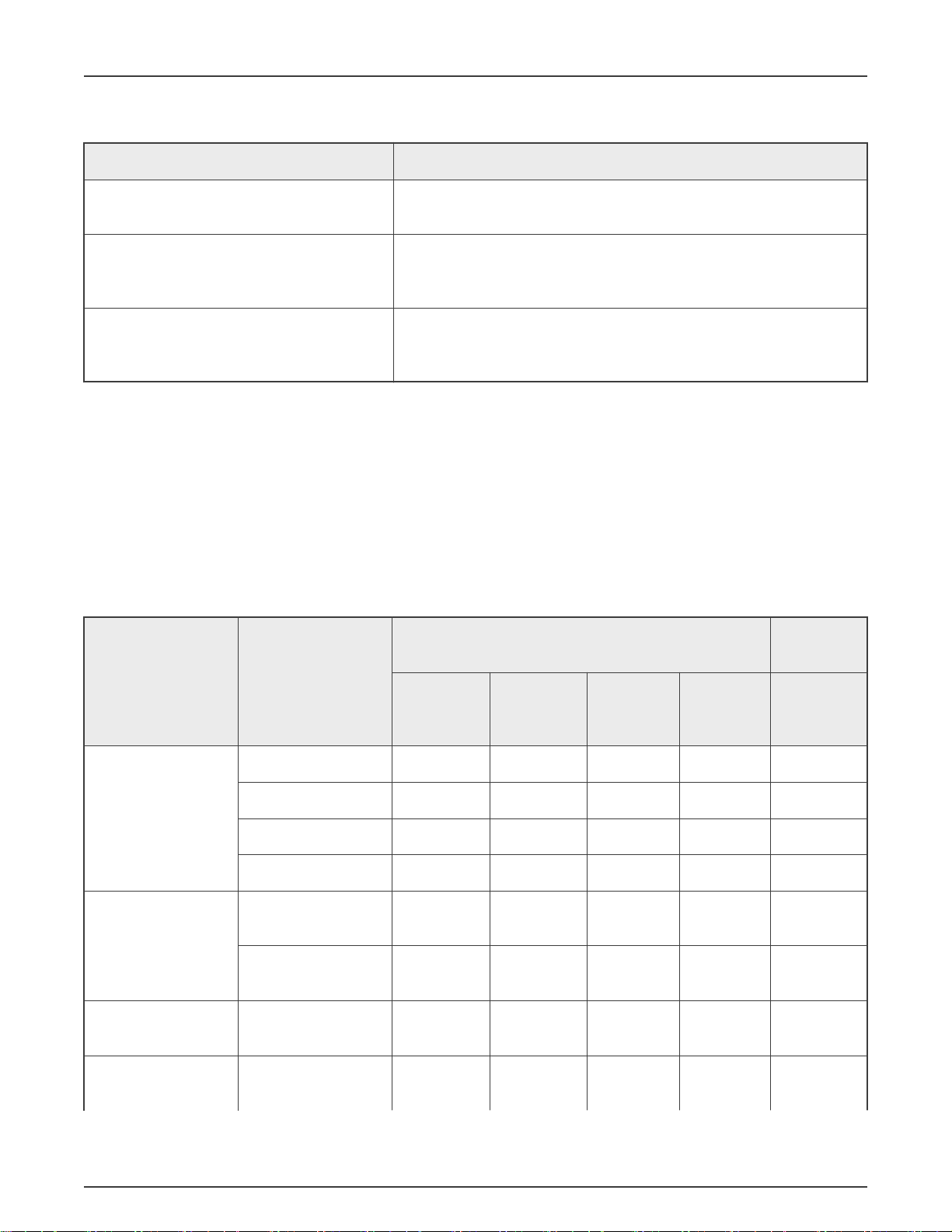
Table 1. Clock and power architecture components
IP module Description
1 Introduction......................................1
2 Clock and power architecture
components.....................................1
3 Low-power modes...........................2
4 Peripherals settings.........................6
5 Creating low-power mode
configuration..................................28
6 Setpoint and CPU mode transition
...................................................... 58
Application Note
Crystal OSC (XTALOSC) The XTALOSC controls the 24-MHz and 32-kHz oscillators. The 24-MHz
crystal oscillator is the primary clock source for all of the PLLs and clock
generation for the CPU and high-speed interfaces. The 32-kHz crystal
oscillator is the primary clock source for the RTC as well as the low-speed
clock source for CCM/SRC/GPC. See the Crystal Oscillator (XTALOSC)
chapter for details on the XTALOSC block.
Clock Control Module (CCM) The CCM module provides control for the clock generation, division,
distribution, synchronization, and coarse-level gating. The CCM contains
also the PLLs and PFDs block, the Clock Root blocks and the Low Peripheral
Clock Gating (LPCG) blocks. The PLLs and their associated PFDs generate
the clocks with various frequencies required to feed the CCM clock generator
that supplies the different functional blocks. The LPCG distributes the clocks
to all blocks in the SoC and handles the automated clock gating and the block
level software-controllable clock gating.
General Power Controller (GPC) The GPC module controls the power state of the whole chip. The GPC
handles the power gating under low-power modes and manages the powerup/power-down sequences.
Power Management Unit (PMU) The PMU module generates internal power supplies distributed to the entire
chip. It controls internal LDOs and body bias options.
Power Gating and Memory Controller (PGMC) The PGMC module controls the power gating of each power domain and the
power state of internal memories.
Table continues on the next page...
Page 2
NXP Semiconductors
Low-power modes
Table 1. Clock and power architecture components (continued)
IP module Description
DCDC Converter (DCDC) The DCDC is a synchronous buck-mode DC-DC converter with two outputs.
The DCDC is used to generate the power supply for the whole chip logic.
System Reset Controller (SRC) The SRC module generates the reset signals for all modules in the
entire chip. The SRC appropriately asserts the reset signals for the power
transitions, entry, and exit.
State Save and Restore Controller (SSARC) The SSARC saves the registers of functional modules in memory before
power down and restores the registers from memory after the module is
powered up.
3 Low-power modes
As mentioned in the previous chapter, i.MX RT1170 provides new power and clock architecture design. Compared to the previous
i.MX RT10xx family MCUs, the i.MX RT1170 power and clock state can be controlled by software, hardware, or combination of
both ways.
Each module can be controlled by software or hardware. For most of the modules, a combination of hardware and software control
is allowed (PGMC, SRC, CCM and PMU). The rest of the modules allows exclusive control by software or hardware (DCDC).
More details are provided later on in this document. See Table 2 for the control options summary. Figure 2 shows the entire
control interconnection.
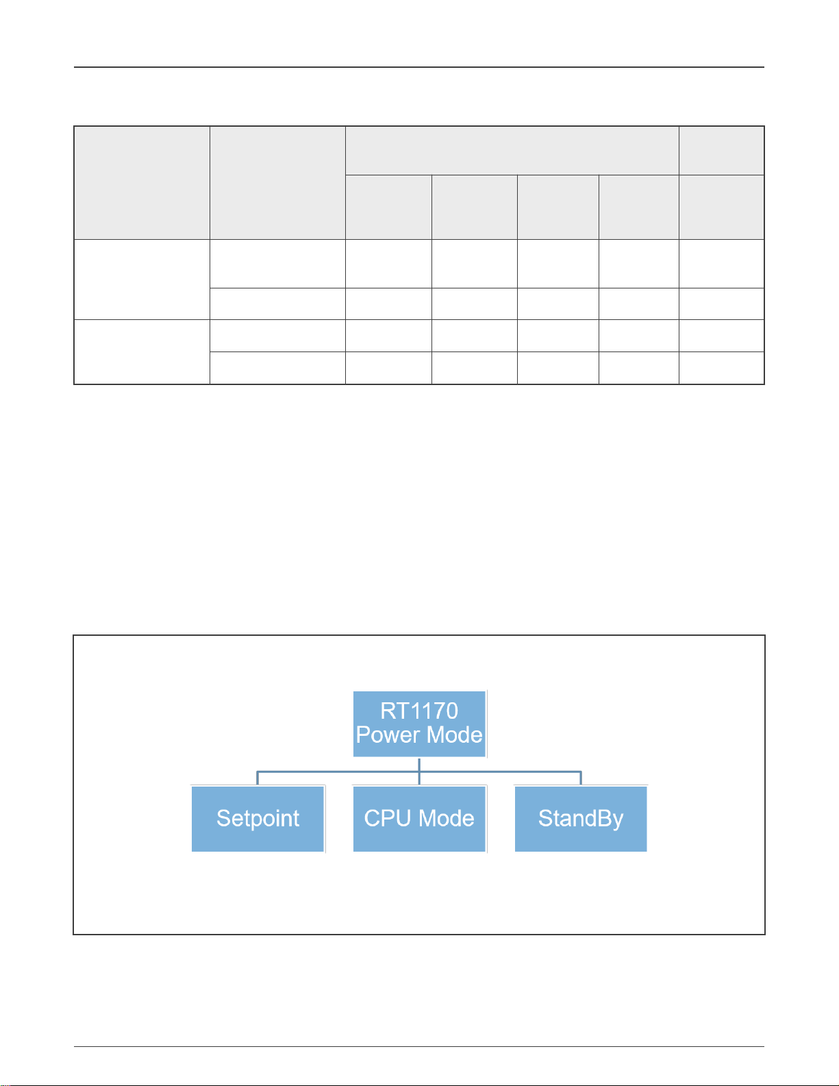
Table 2. Hardware/Software control options overview
Module Module functionality
Enable/Disable √ √
RUN/Low Power mode √ √ √
DCDC
Analog output voltage √ √
Digital output voltage √ √
Power domain
enable/disable
PGMC
Memory low-
power level
SRC
Slice reset
enable/disable
Hardware control mode
CPU mode
control CM7
domain
√ √ √ √
√ √ √ √
√ √ √ √
CPU mode
control CM4
domain
Setpoint
mode control
Standby
mode control
Software
control mode
CCM
Clock sources (PLLs
and oscillators)
√ √ √ √ √
Table continues on the next page...
I.MXRT1170 Low-Power Modes, Rev. 0, 03/2021
Application Note 2 / 59
Page 3
NXP Semiconductors
Table 2. Hardware/Software control options overview (continued)
Low-power modes
Software
control mode
√
Module Module functionality
Clock roots
LPCGs √ √ √ √ √
Body bias √ √ √
PMU
Internal LDOs √ √ √
CPU mode
control CM7
domain
Hardware control mode
CPU mode
control CM4
domain
Setpoint
mode control
√ (not all of
them)
Standby
mode control
3.1 Software control mode
When the software control mode is selected for the appropriate module, the application code becomes responsible for the module
settings and module behavior. The application code must follow all the recommendations, such as the power-up and power-down
sequences, PLL enable sequences, and so on. When any changes of the clock or power settings are requested, the application
code must check if the planned change is valid and ensure that all the changes are executed in a correct order. Otherwise, the
chip behavior can be unpredictable or unstable. The software control is the default control mode of all modules.
3.2 Hardware control mode
When the hardware control mode is selected, the application code determines the hardware control mechanism used for each
resource. i.MX RT1170 allows to control the resources (modules) via the CPU mode control, Setpoint mode control, or Standby
mode control. The final power mode of the whole MCU is defined by the state of the CPUs (Run, Wait, Stop, or Suspend),
preconfigured setpoint (16 setpoints are available), and enabled or disabled Standby mode.
Figure 1. RT1170 power mode
The advantages of the hardware control mode are that the General Power Controller (GPC) takes responsibility for correct
power-up and power-down sequences, setpoints transition sequences, and so on. Even in the hardware control mode, incorrect
settings can be created, but the chip hardware can check most of the consequences and it does not allow the mode transition into
an invalid configuration.
I.MXRT1170 Low-Power Modes, Rev. 0, 03/2021
Application Note 3 / 59
Page 4

NXP Semiconductors
Low-power modes
3.2.1 CPU Mode Control (CMC)
i.MX RT1170 contains two CPU platforms: the Cortex-M7 CPU platform and the Cortex-M4 CPU platform. In case of a single-core
variant, only the Cortex-M7 CPU platform is available. Both CPU platforms support four CPU modes: Run, Wait, Stop, and
Suspend. When the CPU mode control is used for resource control, the resource state is determined by the CPU mode.
The CPU mode transition happens when one of the following events occurs:
• Sleep event: the CPU enters the sleep state with the WFI/WFE instruction
• Wakeup event: an unmasked IRQ wakeup
Both CPU platforms can be in the same CPU mode or in a different CPU mode at the same time. For example, the CM7 CPU
platform is in the Run mode, whereas the CM4 CPU platform is in the Stop mode at the same time. All the combinations are
allowed, but not all of them can be used in applications. Table 2 shows which resources (modules) can be controlled by the CPU
platforms. All the resources that allow the CPU mode control can be controlled by a CPU platform (private resource) or by both
CPU platforms together (shared resource). For more details, see section 14.3.4, Power modes in the Reference Manual.
3.2.2 Setpoint mode control (SPC)
i.MX RT1170 supports 16 setpoints. Setpoints are implemented to control the power state of public resources (resources
which are not owned and controlled by a CPU platform). Table 2 lists the resources that can be controlled by setpoints. For
more information about setpoint transitions triggers, see sections 19.3.2 Setpoint Control (SPC) and 19.3.3 System Setpoint
management in the Reference Manual.
3.2.3 Standby mode control (SBC)
The Standby mode control is a low-power mode that has distinguishing settings outside of the CPU mode control and Setpoint
mode control. The System Standby mode can be entered when the CPU enters the Wait, Stop, or Suspend mode and only when
both CPU platforms send a standby request. The Standby mode control is not supported by all modules. See Table 2 for the list
of the supported modules.
I.MXRT1170 Low-Power Modes, Rev. 0, 03/2021
Application Note 4 / 59
Page 5
NXP Semiconductors
Low-power modes
Figure 2. Resource control options
I.MXRT1170 Low-Power Modes, Rev. 0, 03/2021
Application Note 5 / 59
Page 6
NXP Semiconductors
Peripherals settings
Figure 3. Power architecture overview
4 Peripherals settings
4.1 DCDC settings
The DCDC converter is controlled via software by default. The default DCDC settings are in chapter 21, DCDC Converter in the
Reference Manual.
Table 3 shows all the DCDC features which can be controlled by hardware (Setpoint mode control and Standby mode control)
and which are related to low-power modes. To enable the hardware control mode, set CTRL0 [CONTROL_MODE] = 1. When
the hardware control is enabled, the DCDC parameters are set according to the selected setpoint and the System Standby mode
(enabled or disabled).
The Setpoint mode control and the Standby mode control settings are saved in the registers listed in Table 4. Table 4 also lists
the registers related to the software control mode.
I.MXRT1170 Low-Power Modes, Rev. 0, 03/2021
Application Note 6 / 59
Page 7
NXP Semiconductors
Peripherals settings
Table 3. DCDC general control settings
Functionality Setpoint mode control Standby mode control Software control mode
Enable DCDC output √ √
Enable DCDC_DIG output √ √
Low-power mode/high-power mode √ √ √
VDD 1.8 V Run mode √ √
VDD 1.0 V Run mode √ √
VDD 1.8 V Low power mode √ √ √
VDD 1.0 V Low power mode √ √ √
Table 4. DCDC control settings configuration registers
Hardware control mode Software control mode
CTRL0 [CONTROL_MODE] 1 0
Settings SPC setpoint control SBC standby control
Enable DCDC output REG4 [EANBLE_SP] CTRL0 [ENABLE]
Enable DCDC_DIG output REG5 [EANBLE_SP] CTRL0 [DIG_EN]
Low-power mode/Run mode REG6 [EANBLE_SP]
VDD 1.8 V Run mode target voltage
VDD 1.0 V Run mode target voltage
VDD 1.8 V Low power mode
target voltage
VDD 1.0 V Low power mode
target voltage
[ANA_STBY_TRG_SP_N]
[DIG_STBY_TRG_SP_N]
REG8-11
[ANA_TRG_SP_N]
REG12-15
[DIG_TRG_SP_N]
REG16-19
REG20-23
[STBY_LP_MODE_SP]
REG7P
CTRL0 [LP_MODE_EN]
CTRL1
[VDD1P8CTRL_TRG]
CTRL1
[VDD1P0CTRL_TRG]
CTRL1
[VDD1P8CTRL_STBY_TR
G]
CTRL1
[VDD1P0CTRL_STBY_TR
G]
4.2 Power Gating and Memory Controller (PGMC) settings
The PGMC consists of three submodules which control each power domain. These submodules are the Basic Power Controller
(BPC), CPU Power Controller (CPC), and PMIC Power Controller (PPC). Table 5 shows the general PGMC control options. See
the Reference Manual chapter 20 PGMC for more information about domain assignment.
I.MXRT1170 Low-Power Modes, Rev. 0, 03/2021
Application Note 7 / 59
Page 8

NXP Semiconductors
Table 5. PGMC general control settings
Peripherals settings
CPU mode
control CM7
domain
CPU mode
control CM4
domain
Setpoint mode
control
Standby mode
control
Software control mode
BPC0 - MEGAMIX √ √ √ √
BPC1 - DISPLAYMIX √ √ √ √
BPC2 - WAKEUPMIX √ √ √ √
BPC3 - LPRSMIX √ √ √ √
BPC4 - MIPIPHY √ √ √ √
CPC0 - CM7 core platform √ √ (MLPL only) √
CPC1 - CM4 core platform √ √ (MLPL only) √
PPC0 - PMIC control √ √ √
4.2.1 Basic Power Controller (BPC)
The BPC controls power domains using a simple isolation and power switch (MEGAMIX, DISPLAYMIX, WAKEUPMIX, LPSRMIX,
and MIPIPHY).
The BPC can turn on or shut down the power supply of the domain.
The BPC submodules use the BPC_MODE [CTRL_MODE] register to select which control settings are applied. Every BPC
instance can have different control settings. See Table 5 for the control options list.
If BPC_MODE [CTRL_MODE] = 0x1, thenthe
BPC_POWER_CTRL[PWR_OFF_AT_WAIT],BPC_POWER_CTRL[PWR_OFF_AT_STOP], and
BPC_POWER_CTRL[PWR_OFF_SUSPEND] fields determine the CPU mode in which the power domain is powered off.
The BPC_MODE [DOMAIN_ASSIGN] field selects which CPU mode control is used. Use Domain 0 to select the CM7 domain and
Domain 1 to select the CM4 domain.
If BPC_MODE[CTRL_MODE] = 0x2, then the BPC_POWER_CTRL[PWR_OFF_AT_SP] field determines the setpoints in which
the power domain is powered off.
Table 6. BPC control settings config registers
Software
control
CPU mode control Setpoint
mode control
BPC_MODE [CTRL_MODE] 0 1 2
CM7
domain
CM4
domain
BPC_MODE [DOMAIN_ASSIGN] 0 1
BPC_POWER_CTRL[PSW_ON_SOFT] √
BPC_POWER_CTRL[PSW_OFF_SOFT] √
Table continues on the next page...
I.MXRT1170 Low-Power Modes, Rev. 0, 03/2021
Application Note 8 / 59
Page 9
NXP Semiconductors
Table 6. BPC control settings config registers (continued)
Peripherals settings
Software
control
CPU mode control Setpoint
mode control
BPC_POWER_CTRL[PWR_OFF_AT_WAIT] √ √
BPC_POWER_CTRL[PWR_OFF_AT_STOP] √ √
BPC_POWER_CTRL[PWR_OFF_AT_SUSPEND] √ √
BPC_POWER_CTRL[PWR_OFF_AT_SP] √
The MEGAMIX and DISPLAYMIX power domains are connected to VDD_SOC_IN via a power switch and they can be power
gated separately, even if VDD_SOC_IN is enabled.
The WAKEUPMIX power domain is connected directly to VDD_SOC_IN and can be power gated only if VDD_SOC_IN is disabled
(DCDC_DIG is disabled).
The LPSRMIX is always on the power domain that can be power gated only if the SNVS low-power mode is used. The SNVS
low-power mode is not described in this document. Figure 3 shows the power architecture scheme.
4.2.2 CPU Power Controller (CPC)
The CPC controls the CPU platforms with complex power domain and sequence requirements (CM7 platform and CM4 platform).
The CPC submodules can turn on or shut down the power supply of the CM7 platform and CM4 platform and they allow to set the
cache and TCM memory power level independently of the entire platform. See SW M7-0, 1 and SW LPSR-0, 1 in Figure 3.
For the CM7 platform and CM4 platform control settings, the CPC_CORE_MODE [CTRL_MODE] register is used to select the
control settings to apply. Every CPC instance can use different core settings. See Table 7 for control options.
If CPC_CORE_MODE [CTRL_MODE] = 0x1, thenthe CPC_CORE_POWER_CTRL
[PWR_OFF_AT_WAIT],CPC_CORE_POWER_CTRL [PWR_OFF_AT_STOP], and
CPC_CORE_POWER_CTRL [PWR_OFF_SUSPEND] fields set the CPU mode in which the power domain is powered off.
Table 7. CPC platform control setting configuration registers
Software control mode CPU mode control
CPC Core Mode [CTRL_MODE] 0 1
CMC0 – CM7 core CMC1 – CM4 core
CPC_CORE_POWER_CTRL[PSW_ON_SOFT] √
CPC_CORE_POWER_CTRL[PSW_OFF_SOFT] √
CPC_CORE_POWER_CTRL[PWR_OFF_AT_W
AIT]
CPC_CORE_POWER_CTRL[PWR_OFF_AT_ST
OP]
CPC_CORE_POWER_CTRL[PWR_OFF_AT_S
USPEND]
√ √
√ √
√ √
I.MXRT1170 Low-Power Modes, Rev. 0, 03/2021
Application Note 9 / 59
Page 10

NXP Semiconductors
Peripherals settings
For the cache and TCM memories power level, the CPC_LMEM_MODE [CTRL_MODE] register is used to select which control
method is used. Each CPC instance can use different cache and TCM memory control settings. See Table 8 for the control
options list.
If CPC_LMEM_MODE [CTRL_MODE] = 0x1, then the CPC_LMEM_CM_CTRL [MLPL_AT_RUN],CPC_LMEM_CM_CTRL
[MLPL_AT_WAIT],CPC_LMEM_CM_CTRL [MLPL_AT_STOP], and
CPC_LMEM_CM_CTRL [MLPL_AT_SUSPEND] fields set which memory low-power level option is selected in which CPU mode.
If CPC_LMEM_MODE [CTRL_MODE] = 0x2, then CPC_LMEM_SP0 and CPC_LMEM_SP1 set the memory low-power level
option for the defined setpoint.
Table 8. CPC cache and TCM control setting configuration registers
Software
control mode
CPU mode control
Setpoint mode
control
CPC_LMEM_MODE [CTRL_MODE] 0 1 2
CMC0 - CM7 cache
and TCM
CMC1 - CM4 cache
and TCM
CPC_LMEM_CM_CTRL [MLPL_SOFT] √
CPC_LMEM_CM_CTRL [MLPL_AT_RUN] √ √
CPC_LMEM_CM_CTRL [MLPL_AT_WAIT] √ √
CPC_LMEM_CM_CTRL
[MLPL_AT_STOP]
CPC_LMEM_CM_CTRL
[MLPL_AT_SUSPEND]
√ √
√ √
CPC_LMEM_SP_CTRL_0 √
CPC_LMEM_SP_CTRL_1 √
NOTE
The cache memory for the CM4 core is always powered on and it is not possible to power off the memory via
MLPL settings.
NOTE
The power level of the cache memory and the TCM memory on the CM7 core cannot be controlled separately. The
CPC_LMEM_CM_CTRL or CPC_LMEM_SP_CTRL0/1 registers are used to control both memories together.
For detailed memory low-power level settings, see chapter 20.3.5 Memory Low Power Level in the Reference Manual.
4.2.3 PMIC Power Controller (PPC)
The PPC controls the PMIC standby mode outside of the chip. When the system is in the standby mode, the PPC can send
the PMIC_STBY_REQ to the external PMIC, thus enabling the PMIC to provide a standby voltage. See Table 9 for the PPC
control option.
I.MXRT1170 Low-Power Modes, Rev. 0, 03/2021
Application Note 10 / 59
Page 11
NXP Semiconductors
Peripherals settings
Table 9. PPC control settings config registers
Software control mode Setpoint mode control Standby mode control
Used when the System
PPC_MODE [CTRL_MODE] 0 2
Standby is enabled and
Setpoint mode control
is selected
PPC_STBY_CM_CTRL
[STBY_OFF_SOFT]
PPC_STBY_CM_CTRL
[STBY_ON_SOFT]
PPC_STBY_SP_CTRL
[STBY_ON_AT_SP_ACTIVE]
PPC_STBY_SP_CTRL
[STBY_ON_AT_SP_SLEEP]
√
√
√
√
4.3 Clock Control Module (CCM) settings
The CCM manages the on-chip module clocks. This module allows to set the control for the clock sources (OSCPLL), clock roots,
module clocks (LPCG), and clock groups. Table 10 shows general CCM control options. For detailed information about the CCM,
see the Reference Manual chapter 15 CCM. Detailed control options are discussed later on in this Application note.
Table 10. CCM general control settings
Clock sources
(OSCPLLs)
CPU mode control
CM7 domain
√ √ √ √ √
CPU mode control
CM4 domain
Setpoint
mode control
Standby mode
control
Software
control mode
Clock roots √ √
Module
clocks (LPCGs)
Clock groups √ √
√ √ √ √ √
4.3.1 Module clocks (LPCGs)
The module clocks (LPCGs) support four types of control: unassigned mode, domain mode, CPU low-power mode, and
setpoint mode.
These types are not directly distinguished into the hardware control mode and the software control mode, but the unassigned
mode is considered as software control mode and the CPU low-power mode and the setpoint mode are considered as hardware
control modes.
The domain control mode is not described in this document, because this mode is not directly related to low-power modes. For
more information about the domain control mode, see chapter 15.5.1.2, Domain mode in the Reference Manual. See Table 11 for
the LPCG control options.
I.MXRT1170 Low-Power Modes, Rev. 0, 03/2021
Application Note 11 / 59
Page 12

NXP Semiconductors
Table 11. LPCGs control settings config registers
Software control
mode
(unassigned
mode)
CPU mode control
Setpoint mode
control
Peripherals settings
Standby mode control
LPCG0_DIRECT LPCG137_DIRECT [ON]
LPCG0_AUTHEN LPCG137_AUTHEN [CPULPM]
LPCG0_AUTHEN LPCG137_AUTHEN
[WHITE_LIST]
LPCG0_DOMAIN LPCG137_DOMAIN [LEVEL]
LPCG0_DOMAIN LPCG137_DOMAIN [LEVEL0]
LPCG0_DOMAIN LPCG137_DOMAIN [LEVEL1]
LPCG0_AUTHEN LPCG137_AUTHEN
[SETPOINT_MODE]
x
CM7
domain
CM4 domain
Used when the system
standby is enabled
√ √
√ √
√ √
√
√
√
LPCG2_SETPOINT LPCG12_SETPOINT
√
[SETPOINT]
LPCG2_SETPOINT LPCG12_SETPOINT
√
[STANDBY]
LPCG14_SETPOINT LPCG19_SETPOINT
√
[SETPOINT]
LPCG14_SETPOINT LPCG19_SETPOINT
√
[STANDBY]
LPCG24_SETPOINT LPCG40_SETPOINT
√
[SETPOINT]
Table continues on the next page...
I.MXRT1170 Low-Power Modes, Rev. 0, 03/2021
Application Note 12 / 59
Page 13
NXP Semiconductors
Peripherals settings
Table 11. LPCGs control settings config registers (continued)
Software control
mode
(unassigned
CPU mode control
Setpoint mode
control
Standby mode control
mode)
LPCG24_SETPOINT LPCG40_SETPOINT
√
[STANDBY]
LPCG43_SETPOINT LPCG48_SETPOINT
√
[SETPOINT]
LPCG43_SETPOINT LPCG48_SETPOINT
√
[STANDBY]
4.3.1.1 Unassigned mode
This is the LPCG default mode. After reset, all module clocks are in the unassigned mode. In this mode, the LPCG0_DIRECT –
LPCG137_DIRECT [ON] fields are used for control, if the corresponding module clock is enabled or disabled.
4.3.1.2 CPU Low-Power Mode (CPULPM)
This mode controls the LPCG using the CM7 and CM4 platforms’ status. Before the CPULPM mode is selected, it is recommended
to set the LPCG0_DOMAIN - LPCG137_DOMAIN [LEVELn] fields. These fields determine if module clock is enabled or disabled
according to the CPU status.
The LPCG0_AUTHEN - LPCG137_AUTHEN [CPULPM] fields enable the CPU low-power mode for the appropriate module clock.
The LPCG0_AUTHEN - LPCG137_AUTHEN [WHITE_LIST] fields determine which domain is the owner of the module clock.
None, one, or more domains can be module clock owners. These two bitfields must be set in one step.
The LPCG0_DOMAIN - LPCG137_DOMAIN [LEVELn] fields and the LPCG0_AUTHEN - LPCG137_AUTHEN [WHITE_LIST]
fields determine whether the module clock is enabled or disabled.
If only one domain is the module clock owner, the appropriate LPCG0_DOMAIN - LPCG137_DOMAIN [LEVELn] fields are
used to determine if the corresponding module clock is enabled or disabled in the selected CPU mode. If the module clock is
shared between multiple domains, the LPCG0_DOMAIN - LPCG137_DOMAIN [LEVELn] fields of all domain owners are used
to determine whether the module clock is enabled or disabled. Table 12 shows three configuration examples. Bear in mind the
complexity and possibilities of many configuration options.
Table 12. Module clocks configuration examples
CM7 status
(DOMAIN0)
RUN RUN RUN STOP RUN STOP
LPCGn_AUTHEN
- [WHITE_LIST]
1 (own by CM7) 2 (own by CM4) 3 (own by CM7 and CM4)
CM4 status
(DOMAIN1)
CM7 status
(DOMAIN0)
CM4 status
(DOMAIN1)
CM7 status
(DOMAIN0)
CM4 status
(DOMAIN1)
LPCGn_DOMAIN [LEVEL0] DOMAIN0
1 (enable in RUN mode) 1 (enable in RUN mode) 1 (enable in RUN mode)
Table continues on the next page...
I.MXRT1170 Low-Power Modes, Rev. 0, 03/2021
Application Note 13 / 59
Page 14
NXP Semiconductors
Table 12. Module clocks configuration examples (continued)
LPCGn_DOMAIN [LEVEL1] DOMAIN1
1 (enable in RUN mode) 1 (enable in RUN mode) 0 (always disable)
clock settings
Peripherals settings
Resulting module n clock
enable/disable
Enable - Module clock is
owned by CM7 core which
is in RUN mode, so per
LEVEL0 configuration the clock
is enabled.
Disable - – Module clock is
owned by CM4 core which
is in STOP mode, so per
LEVEL1 configuration the
clock is disabled
Enable - Module clock is owned
by both cores. CM7 is in the
“highest” modes, so per LEVEL0
configuration the clock is enabled.
4.3.1.3 Setpoint mode
The setpoint mode controls the LPCG using the selected setpoint. Not all LPCGs support the setpoint mode control. The supported
LPCGs are LPCG2 – LPCG12, LPCG14 – LPCG19, LPCG24 – LPCG40, and LPCG43 – LPCG48.
The LPCG0_AUTHEN - LPCG137_AUTHEN [SETPOINT_MODE] fields enable the setpoint mode for the appropriate module
clock. The LPCG2_SETPOINT - LPCG48_SETPOINT [SETPOINT] fields determine in which setpoint is the module clock enabled
or disabled.
The module clocks that support the setpoint mode can be also controlled by the system standby when the setpoint mode is
selected. The LPCG2_SETPOINT - LPCG48_SETPOINT [STANDBY] fields determine whether the module clock is enabled or
disabled when the system enters the standby mode.
4.3.2 Clock sources (OSCPLLs)
The clock sources (OSCPLLs) support four types of control: unassigned mode, domain mode, CPU low-power mode, and
setpoint mode.
The OSCPLLs distinguish between the hardware control mode and the software control mode. These modes can be switched
using the CTRL registers listed in Table 13. When the software control mode is selected, the clock sources are controlled by the
CCM PLL registers and the XTALOSC registers. The settings in the OSCPLL_0 – OSCPLL_28 registers do not have any effect.
The domain mode control is not described in this application note, because this mode is not related to low-power modes. For more
information about the domain mode, see chapter 15.5.1.2 Domain mode in the Reference Manual. See Table 13 for the OSCPLL
control possibilities.
Table 13. OSCPLLs control settings config registers
Software
control
Hardware control mode
mode
ARM_PLL_CTRL
[ARM_PLL_CONTROL_MODE]
SYS_PLL1_CTRL
[SYS_PLL1_CONTROL_MODE]
Unassigned
mode
CPU mode control
0 1
0 1
Setpoint
mode
control
Standby
mode
control
Table continues on the next page...
I.MXRT1170 Low-Power Modes, Rev. 0, 03/2021
Application Note 14 / 59
Page 15

NXP Semiconductors
Table 13. OSCPLLs control settings config registers (continued)
Peripherals settings
SYS_PLL2_CTRL
[SYS_PLL2_CONTROL_MODE]
SYS_PLL3_CTRL
[SYS_PLL3_CONTROL_MODE]
PLL_AUDIO_CTRL
[PLL_AUDIO_CONTROL_MODE]
PLL_VIDEO_CTRL
[PLL_VIDEO_CONTROL_MODE]
OSC_400M_CTRL1
[RC_400M_CONTROL_MODE]
OSC_48M_CTRL
[RC_48M_CONTROL_MODE]
OSC_48M_CTRL
[RC_48M_DIV2_CONTROL_MODE]
OSC_16M_CTRL
[RC_16M_CONTROL_MODE]
OSC_24M_CTRL
[OSC_24M_CONTROL_MODE]
0 1
0 1
0 1
0 1
0 1
0 1
0 1
0 1
0 1
OSCPLL0_DIRECT OSCPLL28_DIRECT [ON]
OSCPLL0_AUTHEN OSCPLL28_AUTHEN [CPULPM]
OSCPLL0_AUTHEN OSCPLL28_AUTHEN [WHITE_LIST]
OSCPLL0_DOMAIN OSCPLL28_DOMAIN [LEVEL]
OSCPLL0_DOMAIN OSCPLL28_DOMAIN [LEVEL0]
OSCPLL0_DOMAIN OSCPLL28_DOMAIN [LEVEL1]
OSCPLL0_AUTHEN OSCPLL28_AUTHEN [SETPOINT_MODE]
√
domain
Table continues on the next page...
CM7
√ √
√ √
√ √
√
CM4
domain
√
√
I.MXRT1170 Low-Power Modes, Rev. 0, 03/2021
Application Note 15 / 59
Page 16

NXP Semiconductors
Table 13. OSCPLLs control settings config registers (continued)
Peripherals settings
OSCPLL0_SETPOINT OSCPLL28_SETPOINT [SETPOINT]
OSCPLL0_SETPOINT OSCPLL28_SETPOINT [STANDBY]
√
√
4.3.2.1 Unassigned mode
In this mode, the OSCPLL0_DIRECT - OSCPLL28_DIRECT [ON] fields are used to control whether the clock source is enabled
or disabled.
4.3.2.2 CPU Low-Power Mode (CPULPM)
This mode controls the OSCPLLs using the CM7 and CM4 platforms’ status. Before the CPULPM mode is selected, it is
recommended to set the OSCPLL0_DOMAIN – OSCPLL28_DOMAIN [LEVELn] fields. These fields determine whether the
module clock is enabled or disabled according to the CPU status.
The OSCPLL0_AUTHEN – OSCPLL28_AUTHEN [CPULPM] fields enable the CPULPM for the appropriate module clock. The
OSCPLL0_AUTHEN – OSCPLL28_AUTHEN [WHITE_LIST] fields determine which domain is the owner of the module clock.
None, one, or more domains can be the module clock owners. These two bits must be set in one step.
The OSCPLL0_DOMAIN – OSCPLL28_DOMAIN [LEVELn] fields and OSCPLL0_AUTHEN – OSCPLL28_AUTHEN
[WHITE_LIST] fields determine whether the module clock is enabled or disabled. These settings are the same as those
for the LPCG. See the previous chapter and Table 12 for more details.
4.3.2.3 Setpoint mode
This mode controls the OSCPLLs using the selected setpoint. The OSCPLL0_AUTHEN – OSCPLL28_AUTHEN
[SETPOINT_MODE] fields enable the setpoint mode for the appropriate module clock. The OSCPLL0_SETPOINT – OSCPLL28
[SETPOINT] fields determine in which setpoints the corresponding clock source is enabled or disabled.
The Clock sources that support the setpoint mode can be also controlled by the system standby when the setpoint mode is
selected. The OSCPLL0_SETPOINT – OSCPLL28 [STANDBY] fields determine whether the clock source is enabled or disabled
when the system enters the standby mode.
4.3.3 Clock roots
The clock roots support three types of control: unassigned mode, domain mode, and setpoint mode.
These types are not directly distinguished into the hardware control mode and the software control mode, but the unassigned
mode is the software control mode and the setpoint mode is the hardware control mode.
The domain mode control is not described in this application note, because this mode is not directly related to low-power modes.
For more information about the domain mode, see chapter 15.5.1.2 Domain mode in the Reference Manual. See Table 14 for the
clock roots control possibilities.
Table 14. Clock roots control settings config registers
CLOCK_ROOT0_CONTROL
- CLOCK_ROOT78_CONTROL
Software control mode
(unassigned mode)
√
Setpoint mode control
Table continues on the next page...
I.MXRT1170 Low-Power Modes, Rev. 0, 03/2021
Application Note 16 / 59
Page 17
NXP Semiconductors
Table 14. Clock roots control settings config registers (continued)
Peripherals settings
CLOCK_ROOT0_AUTHEN CLOCK_ROOT78_AUTHEN [SETPOINT_MODE]
CLOCK_ROOT0_SETPOINT0
- CLOCK_ROOT78_SETPOINT15
Software control mode
(unassigned mode)
Setpoint mode control
√
√
4.3.3.1 Unassigned mode
This is the clock roots default mode. After a reset, all clock roots are in the unassigned mode. In this mode, the
CLOCK_ROOT0_CONTROL - CLOCK_ROOT78_CONTROL registers are used to set up the clock roots settings (OFF,
MUX, DIV).
4.3.3.2 Setpoint mode
This mode controls the clock roots using the selected setpoint. Not all clock roots support the setpoint mode control. The
supported clock roots are CLOCK_ROOT0 – CLOCK_ROOT4, CLOCK_ROOT20 – CLOCK_ROOT21, and CLOCK_ROOT77
– CLOCK_ROOT78.
The CLOCK_ROOT0_AUTHEN - CLOCK_ROOT78_AUTHEN [SETPOINT_MODE] fields enable the setpoint mode for the
appropriate clock root. The CLOCK_ROOT0_SETPOINT0 -CLOCK_ROOT78_SETPOINT15 registers are used to set up the
clock root settings (GRADE, OFF, MUX, DIV).
4.3.4 Clock groups
The clock groups support three types of control: unassigned mode, domain mode, and setpoint mode.
These types are not directly distinguished into the hardware control mode and the software control mode, but the unassigned
mode is the software control and the setpoint mode is the hardware control.
The domain mode control is not described in this application note, because this mode is not related to low-power modes. For more
information about the domain mode, see chapter 15.5.1.2 Domain mode in the Reference Manual. See Table 15 for the clock
groups’ control possibilities.
Table 15. Clock groups control settings config registers
CLOCK_GROUP0_CONTROL
- CLOCK_GROUP1_CONTROL
CLOCK_GROUP0_AUTHEN CLOCK_GROUP1_AUTHEN [SETPOINT_MODE]
CLOCK_GROUP0_SETPOINT0
- CLOCK_GROUP1_SETPOINT15
4.3.4.1 Unassigned mode
Software control mode
(Unassigned mode)
√
Setpoint mode control
√
√
This is the default clock groups mode. After a reset, all clock groups are in the unassigned mode. In this mode, the
CLOCK_GROUP0_CONTROL - CLOCK_GROUP1_CONTROL registers are used to set up the clock groups’ settings (OFF,
RSTDIV, DIV0).
I.MXRT1170 Low-Power Modes, Rev. 0, 03/2021
Application Note 17 / 59
Page 18
NXP Semiconductors
Peripherals settings
4.3.4.2 Setpoint mode
The CLOCK_GROUP0_AUTHEN - CLOCK_GROUP1_AUTHEN [SETPOINT_MODE] fields enable the setpoint mode for the
appropriate clock group. The CLOCK_GROUP0_SETPOINT0 -CLOCK_GROUP1_SETPOINT15 registers are used to set up the
clock groups’ settings (GRADE, OFF, RSTDIV, DIV0).
4.4 PMU settings
The Power Management Unit (PMU) is comprised of the following components integrated for the power management. One DCDC
module generates the core power supply, the LDOs generate power for the internal logics, and multiple power switches create
sophisticated power mode management. Table 16 shows general PMU control possibilities. For a detailed schema of the power
architecture, see Figure 3. For more information about the PMU, see the Reference Manual chapter 17.
NOTE
The software mode supports flexible control, but pay attention to the analog dependencies and power structure
sequences. In the Hardware control mode, everything is handled precisely by hardware.
Table 16. PMU general control settings
Setpoint mode control Standby mode control
Software
control mode
PLL LDO √ √ √
LPSR ANA LDO √ √ √
LPSR DIG LDO √ √ √
BANDGAP √ √ √
BODY BIAS √ √ √
4.4.1 PLL LDO
The PLL LDO is used to power the system PLLs. The PMU_LDO_PLL [LDO_PLL_CONTROL_MODE] field is used to select the
control method that are applied. See Table 17 for the control options.
If PMU_LDO_PLL [LDO_PLL_CONTROL_MODE] = 0x0, then the
PMU_LDO_PLL [LDO_PLL_ENABLE] field is used to switch the LDO on or off manually.
If PMU_LDO_PLL [LDO_PLL_CONTROL_MODE] = 0x1, then the
LDO_PLL_ENABLE_SP [ON_OFF_SETPOINTn] and
PLL_LDO_STBY_EN_SP [STBY_EN_SETPOINTn] fields are used to select in which setpoint the LDO is enabled and whether the
LDO is enabled when the system enters the standby mode.
Table 17. PLL LDO control settings config registers
Software control mode Hardware control mode
Setpoint
mode control
Standby
mode control
PMU_LDO_PLL [LDO_PLL_CONTROL_MODE] 0 1
PMU_LDO_PLL [LDO_PLL_ENABLE] √
Table continues on the next page...
I.MXRT1170 Low-Power Modes, Rev. 0, 03/2021
Application Note 18 / 59
Page 19

NXP Semiconductors
Peripherals settings
Table 17. PLL LDO control settings config registers (continued)
Software control mode Hardware control mode
LDO_PLL_ENABLE_SP [ON_OFF_SETPOINTn] √
PLL_LDO_STBY_EN_SP [STBY_EN_SETPOINTn] √
4.4.2 LPSR ANA LDO
The LPSR ANA LDO is used to power the analog part of the LPSR power domain when the DCDC converter is bypassed or if a
different power supply is required from the SoC power domain for the LPSR power domain.
The [LDO_PLL_CONTROL_MODE] field is used to select the control settings that are applied. See Table 18 for the control options.
If PMU_LDO_LPSR_ANA [LPSR_ANA_CONTROL_MODE] = 0x0, then the
PMU_LDO_LPSR_ANA [REG_DISABLE],
PMU_LDO_LPSR_ANA [TRACK_MODE_EN],
PMU_LDO_LPSR_ANA [BYPASS_MODE_EN], and
PMU_LDO_LPSR_ANA [REG_LP_EN] fields are used to control the LPSR ANA LDO settings manually (enable/disable, bypass,
tracking mode, low-power mode).
If PMU_LDO_LPSR_ANA [LPSR_ANA_CONTROL_MODE] = 0x1, then the
LDO_LPSR_ANA_ENABLE_SP [ON_OFF_SETPOINTn],
LDO_LPSR_ANA_LP_MODE_SP [LP_MODE_SETPONITn],
LDO_LPSR_ANA_TRACKING_EN_SP [TRACKING_EN_SETPOINTn],
LDO_LPSR_ANA_BYPASS_EN_SP [BYPASS_EN_SETPOINTn], and
LDO_LPSR_ANA_STBY_EN_SP [STBY_EN_SETPOINTn] fields are used to create the LDO settings for the appropriate setpoint.
The STBY_EN_SETPOINTn bitfield determines whether the LDO is in the HP or LP mode when the system enters the
stanby mode.
Table 18. LPSR ANA LDO control settings config registers
Software control mode Hardware control mode
PMU_LDO_LPSR_ANA
[LPSR_ANA_CONTROL_MODE]
Setpoint
mode control
0 1
Standby
mode control
PMU_LDO_LPSR_ANA [REG_DISABLE] √
PMU_LDO_LPSR_ANA [TRACK_MODE_EN] √
PMU_LDO_LPSR_ANA [BYPASS_MODE_EN] √
PMU_LDO_LPSR_ANA [REG_LP_EN] √
LDO_LPSR_ANA_ENABLE_SP
[ON_OFF_SETPOINTn]
√
Table continues on the next page...
I.MXRT1170 Low-Power Modes, Rev. 0, 03/2021
Application Note 19 / 59
Page 20

NXP Semiconductors
Peripherals settings
Table 18. LPSR ANA LDO control settings config registers (continued)
Software control mode Hardware control mode
LDO_LPSR_ANA_LP_MODE_SP
[LP_MODE_SETPONITn]
LDO_LPSR_ANA_TRACKING_EN_SP
[TRACKING_EN_SETPOINTn]
LDO_LPSR_ANA_BYPASS_EN_SP
[BYPASS_EN_SETPOINTn]
LDO_LPSR_ANA_STBY_EN_SP
[STBY_EN_SETPOINTn]
√
√
√
√
4.4.3 LPSR DIG LDO
The LPSR AND LDO is used to power the digital part of LPSR power domain when the DCDC converter is bypassed or a different
power supply from the SoC power domain is required for the LPSR power domain.
The PMU_LDO_LPSR_DIG [LPSR_DIG_CONTROL_MODE] field is used to select which control settings are applied. See Table
19 for the control options.
If PMU_LDO_LPSR_DIG [LPSR_DIG_CONTROL_MODE] = 0x0, then the
PMU_LDO_LPSR_DIG [REG_EN],
PMU_LDO_LPSR_DIG [TRACKING_MODE],
PMU_LDO_LPSR_DIG [BYPASS_MODE], and
PMU_LDO_LPSR_DIG [VOLTAGE_SELECT] fields are used to control the LPSR DIG LDO settings manually (enable/disable,
bypass, tracking mode, voltage level).
If PMU_LDO_LPSR_DIG [LPSR_DIG_CONTROL_MODE] = 0x1, then the
LDO_LPSR_DIG_ENABLE_SP [ON_OFF_SETPOINTn],
LDO_LPSR_DIG_LP_MODE_SP [LP_MODE_SETPONITn],
LDO_LPSR_DIG_TRACKING_EN_SP [TRACKING_EN_SETPOINTn],
LDO_LPSR_DIG_BYPASS_EN_SP [BYPASS_EN_SETPOINTn],
LDO_LPSR_DIG_STBY_EN_SP [STBY_EN_SETPOINTn],
LDO_LPSR_DIG_TRG_SP0 [VOLTAGE_SETPOINTn],
LDO_LPSR_DIG_TRG_SP1 [VOLTAGE_SETPOINTn],
LDO_LPSR_DIG_TRG_SP2 [VOLTAGE_SETPOINTn],
LDO_LPSR_DIG_TRG_SP3 [VOLTAGE_SETPOINTn], and
LDO_LPSR_DIG_STBY_EN_SP [STBY_EN_SETPOINTn] fields are used to create the LDO settings for the appropriate setpoint.
The STBY_EN_SETPOINTn bitfield determines whether the LDO is in the HP or LP mode when the system enters the
stanby mode.
I.MXRT1170 Low-Power Modes, Rev. 0, 03/2021
Application Note 20 / 59
Page 21

NXP Semiconductors
Peripherals settings
Table 19. LPSR DIG LDO control settings config registers
Software control mode Hardware control mode
PMU_LDO_LPSR_DIG
[LPSR_DIG_CONTROL_MODE]
PMU_LDO_LPSR_DIG [REG_EN] √
PMU_LDO_LPSR_DIG [TRACKING_MODE] √
PMU_LDO_LPSR_DIG [BYPASS_MODE] √
PMU_LDO_LPSR_DIG [VOLTAGE_SELECT] √
LDO_LPSR_DIG_ENABLE_SP
[ON_OFF_SETPOINTn]
LDO_LPSR_DIG_LP_MODE_SP
[LP_MODE_SETPONITn]
LDO_LPSR_DIG_TRACKING_EN_SP
[TRACKING_EN_SETPOINTn]
LDO_LPSR_DIG_BYPASS_EN_SP
[BYPASS_EN_SETPOINTn]
Setpoint
mode control
0 1
√
√
√
√
Standby
mode control
LDO_LPSR_DIG_STBY_EN_SP
[STBY_EN_SETPOINTn]
√
LDO_LPSR_DIG_TRG_SP0 [VOLTAGE_SETPOINTn] √
LDO_LPSR_DIG_TRG_SP1 [VOLTAGE_SETPOINTn] √
LDO_LPSR_DIG_TRG_SP2 [VOLTAGE_SETPOINTn] √
LDO_LPSR_DIG_TRG_SP3 [VOLTAGE_SETPOINTn] √
LDO_LPSR_DIG_STBY_EN_SP
[STBY_EN_SETPOINTn]
√
4.4.4 BANDGAP
The PMU_REF_CTRL [REF_CONTROL_MODE] field is used to select which control scheme is applied. See Table 20 for the
BANDGAP control options.
If PMU_REF_CTRL [REF_CONTROL_MODE] = 0x0, then the
PMU_REF_CTRL [REF_ENABLE] field is used to switch the BANDGAP on or off manually.
If PMU_REF_CTRL [REF_CONTROL_MODE] = 0x1, then the
BANDGAP_ENABLE_SP [ON_OFF_SETPOINTn] and
I.MXRT1170 Low-Power Modes, Rev. 0, 03/2021
Application Note 21 / 59
Page 22

NXP Semiconductors
Peripherals settings
BANDGAP_STBY_EN_SP [STBY_EN_SETPOINTn] fields are used to select in which setpoint is the BANDGAP enabled and if
the BANDGAP is enabled when the system enters the Standby mode.
Table 20. BANDGAP control settings config registers
Software control mode Hardware control mode
Setpoint
mode control
Standby
mode control
PMU_REF_CTRL [REF_CONTROL_MODE] 0 1
PMU_REF_CTRL [REF_ENABLE] √
BANDGAP_ENABLE_SP [ON_OFF_SETPOINTn] √
BANDGAP_STBY_EN_SP [STBY_EN_SETPOINTn] √
4.4.5 Body Bias
The Forward Body Biasing (FBB) and Reverse Body Biasing (RBB) are implemented to boost the performance
and reduce the power respectively. The PMU_BIAS_CTRL [RBB_LPSR_CONTROL_MODE], PMU_BIAS_CTRL
[RBB_SOC_CONTROL_MODE], and PMU_BIAS_CTRL [FBB_M7_CONTROL_MODE] fields are used to select which control
scheme is applied. See Table 21 for the Body Bias control options.
If PMU_BIAS_CTRL [RBB_LPSR_CONTROL_MODE], PMU_BIAS_CTRL [RBB_SOC_CONTROL_MODE], and
PMU_BIAS_CTRL [FBB_M7_CONTROL_MODE] = 0x0, then thePMU_BIAS_CTRL2 [WB_EN] and
PMU_BIAS_CTRL2 [WB_PWR_SW_EN_1P8] fields are used to enable the Body Bias. The software must ensure that the FBB
and RBB are not enabled simultaneously, because only one can be used at a time.
If PMU_BIAS_CTRL [RBB_LPSR_CONTROL_MODE], PMU_BIAS_CTRL [RBB_SOC_CONTROL_MODE] and
PMU_BIAS_CTRL [FBB_M7_CONTROL_MODE] = 0x1, then the
FBB_M7_ENABLE_SP [ON_OFF_SETPOINTn],
RBB_SOC_ENABLE_SP [ON_OFF_SETPOINTn],
RBB_LPSR_ENABLE_SP [ON_OFF_SETPOINTn],
FBB_M7_STBY_EN_SP [STBY_EN_SETPOINTn],
RBB_SOC_STBY_EN_SP [STBY_EN_SETPOINTn], and
RBB_LPSR_STBY_EN_SP [STBY_EN_SETPOINTn] fields are used to create the Body Bias settings for the appropriate setpoint.
Only one Body Bias can be used at a time.
The combination of the software and hardware control modes for single body biases is allowed but it is not recommended.
Table 21. Body Bias control settings config registers
Software control mode Hardware control mode
Setpoint
mode control
Standby
mode control
PMU_BIAS_CTRL [RBB_LPSR_CONTROL_MODE] 0 1
PMU_BIAS_CTRL [RBB_SOC_CONTROL_MODE] 0 1
Table continues on the next page...
I.MXRT1170 Low-Power Modes, Rev. 0, 03/2021
Application Note 22 / 59
Page 23

NXP Semiconductors
Peripherals settings
Table 21. Body Bias control settings config registers (continued)
Software control mode Hardware control mode
PMU_BIAS_CTRL [FBB_M7_CONTROL_MODE] 0 1
PMU_BIAS_CTRL2 [WB_EN] √
PMU_BIAS_CTRL2 [WB_PWR_SW_EN_1P8] √
FBB_M7_ENABLE_SP [ON_OFF_SETPOINTn] √
RBB_SOC_ENABLE_SP [ON_OFF_SETPOINTn] √
RBB_LPSR_ENABLE_SP [ON_OFF_SETPOINTn] √
FBB_M7_STBY_EN_SP [STBY_EN_SETPOINTn] √
RBB_SOC_STBY_EN_SP [STBY_EN_SETPOINTn] √
RBB_LPSR_STBY_EN_SP [STBY_EN_SETPOINTn] √
4.5 SRC settings
The System Reset Controller (SRC) is responsible for the generation of all the system reset signals and boot argument
latching. The reset control determines the source and type of reset and performs the necessary reset qualification and
stretching sequences.
The SRC receives reset requests from all the potential reset sources and generates the Slice Root Reset to the reset slices (Slice
Reset Control). The Slice Reset Control helps to determine the reset behavior according to the slice configuration and the system
low-power status after the slice root reset de-assertion. There are 10 independent reset domains in the system. Correspondingly,
there are 10 dedicated reset slices. The reset slices generate the dedicated reset signal for each reset domain. Table 22 lists all
reset slices and their control settings possibilities.
Table 22. Reset Slices - General control settings
CPU mode control CM7 CPU mode control CM4 Setpoint mode control Software
control mode
MEGA √ √ √ √
DISPLAY √ √ √ √
WAKEUP √ √ √ √
LPSR √ √ √ √
M4CORE √ √ √ √
M7CORE √ √ √ √
M4DEBUG √ √ √ √
M7DEBUG √ √ √ √
Table continues on the next page...
I.MXRT1170 Low-Power Modes, Rev. 0, 03/2021
Application Note 23 / 59
Page 24

NXP Semiconductors
Peripherals settings
Table 22. Reset Slices - General control settings (continued)
CPU mode control CM7 CPU mode control CM4 Setpoint mode control Software
control mode
USBPHY1 √ √ √ √
USBPHY2 √ √ √ √
For the reset slice using software, use the CTRL_MEGA - CTRL_USBPHY2 [SW_RESET] field in the appropriate register. Writing
1 into the SW_RESET field executes a slice reset.
For the CPU mode control, the AUTHEN_MEGA - AUTHEN_USBPHY2 [DOMAIN_MODE] field must be set and the control
domain must be selected using AUTHEN_MEGA - AUTHEN_USBPHY2 [ASSIGN_LIST]. It is allowed to set more than one
domain to control a reset slice. In this case, all selected domains can trigger a slice reset.
The DOMAIN_MEGA - DOMAIN_USBPHY2 [CPU0_RUN],
DOMAIN_MEGA - DOMAIN_USBPHY2 [CPU0_WAIT],
DOMAIN_MEGA - DOMAIN_USBPHY2 [CPU0_STOP], and
DOMAIN_MEGA - DOMAIN_USBPHY2 [CPU0_SUSP] fields are used to select which mode transition triggers the slice reset.
For the Setpoint mode control, the AUTHEN_MEGA - AUTHEN_USBPHY2 [SETPOINT_MODE] field must be set. The
SETPOINT_MEGA - SETPOINT_USBPHY2 [SETPOINTn] fields are used to determine which setpoint transition triggers the
slice reset.
Table 23. Reset slices control settings config registers
CTRL_MEGA CTRL_USBPHY2 [SW_RESET]
Software
control mode
√
CPU mode control
CM7 domain CM4 domain
AUTHEN_MEGA AUTHEN_USBPHY2
√ √
[DOMAIN_MODE]
AUTHEN_MEGA AUTHEN_USBPHY2 [ASSIGN_LIST]
DOMAIN_MEGA DOMAIN_USBPHY2 [CPU0_RUN]
DOMAIN_MEGA DOMAIN_USBPHY2 [CPU0_WAIT]
DOMAIN_MEGA DOMAIN_USBPHY2 [CPU0_STOP]
√ √
√
√
√
Setpoint mode
control
DOMAIN_MEGA DOMAIN_USBPHY2 [CPU0_SUSP]
√
Table continues on the next page...
I.MXRT1170 Low-Power Modes, Rev. 0, 03/2021
Application Note 24 / 59
Page 25

NXP Semiconductors
Table 23. Reset slices control settings config registers (continued)
Peripherals settings
DOMAIN_MEGA DOMAIN_USBPHY2 [CPU1_RUN]
DOMAIN_MEGA DOMAIN_USBPHY2 [CPU1_WAIT]
DOMAIN_MEGA DOMAIN_USBPHY2 [CPU1_STOP]
DOMAIN_MEGA DOMAIN_USBPHY2 [CPU1_SUSP]
AUTHEN_MEGA AUTHEN_USBPHY2
[SETPOINT_MODE]
SETPOINT_MEGA SETPOINT_USBPHY2 [SETPOINTn]
√
√
√
√
√
√
4.6 GPC settings
The General Power Controller (GPC) is the centralized power controller, which controls the power mode of the processor. The
GPC takes the Wait For Interrupt (WFI) signal from the CPU platforms and the wakeup events from the peripherals to determine
the power mode based on the GPC power management policy. The GPC also controls the power mode transition.
The GPC contains four sub-modules: CPU Mode Control (CMC), Setpoint Control (SPC), Standby Control (SBC), and Unified
Power Management Interface (UPI) . See Figure 1 for a detailed interconnection of single peripherals to the GPC unit. The GPC
unit shown in Figure 1 does not contain a UPI sub-module. Understanding the UPI functionality is not critical for low-power modes’
settings. For simplification, it is excluded from the interconnection schema. For more information about the UPI, see chapter 19.3
Unified power management interface (UPI) in the Reference Manual.
4.6.1 CPU Mode Control (CMC)
There are two CMC submodules available. CMC0 contains the CPU mode controller for the CM7 platform and CMC1 contains
the CPU mode controller for the CM4 platform. These CMCs control the CPU modes of the CPU platforms and their private
resources. Both CMCs can have different settings. For more details about the CMC, see chapter 19.3.1 CPU Mode Control in the
Reference Manual. See Table 24 for a list of low-power-mode-related CMC features and appropriate configuration registers. See
the Reference Manual chapter 19.3.6.1 CPU mode transition flow, which is directly related to the registers in Table 24.
Table 24. CMC low-power-mode-related settings config registers
Settings description Register
CM_SLEEP_SSAR_CTRL
CM_SLEEP_LPCG_CTRL
CMC-controlled resources sleep settings
CM_SLEEP_PLL_CTRL
CM_SLEEP_ISO_CTRL
CM_SLEEP_RESET_CTRL
Table continues on the next page...
I.MXRT1170 Low-Power Modes, Rev. 0, 03/2021
Application Note 25 / 59
Page 26
NXP Semiconductors
Table 24. CMC low-power-mode-related settings config registers (continued)
Settings description Register
CM_SLEEP_POWER_CTRL
CM_WAKEUP_POWER_CTRL
CM_WAKEUP_RESET_CTRL
CM_WAKEUP_ISO_CTRL
CMC-controlled resources wakeup settings
CM_WAKEUP_PLL_CTRL
CM_WAKEUP_LPCG_CTRL
CM_WAKEUP_SSAR_CTRL
Setpoint transition control settings CM_SP_CTRL
CM_RUN_MODE_MAPPING
Peripherals settings
CM_WAIT_MODE_MAPPING
Allowed setpoints for appropriate CPU mode
CM_STOP_MODE_MAPPING
CM_SUSPEND_MODE_MAPPING
Setpoint mapping register CM_SP0_MAPPING - CM_SP15_MAPPING
4.6.2 Setpoint Control (SPC)
The GPC supports 16 Setpoints. Setpoints are implemented to configure the power state of Public Resources. Public Resources
are system-level resources that are not owned or controlled by any CPU platforms. The Setpoint transition is triggered by a request
from any CPU platforms. For more details about the SPC, see chapter 19.3.2 Setpoint Control in the Reference Manual. See Table
25 for a list of low-power-mode-related SPC features and appropriate configuration registers. See the Reference Manual chapter
19.3.6.2 Setpoint transition flow, which is directly related to the registers in Table 25.
Table 25. SPC low-power-mode-related settings config registers
Settings description Register
RCOS16M control settings SP_ROSC_CTRL
SP_SSAR_SAVE_CTRL
SP_LPCG_OFF_CTRL
SPC-controlled resources sleep settings
SP_GROUP_DOWN_CTRL
SP_ROOT_DOWN_CTRL
SP_PLL_OFF_CTRL
Table continues on the next page...
I.MXRT1170 Low-Power Modes, Rev. 0, 03/2021
Application Note 26 / 59
Page 27

NXP Semiconductors
Table 25. SPC low-power-mode-related settings config registers (continued)
Settings description Register
SP_ISO_ON_CTRL
SP_RESET_EARLY_CTRL
SP_POWER_OFF_CTRL
SP_BIAS_OFF_CTRL
SP_BG_PLDO_OFF_CTRL
SP_LDO_PRE_CTRL
SP_DCDC_DOWN_CTRL
SP_DCDC_UP_CTRL
SP_LDO_POST_CTRL
Peripherals settings
SP_BG_PLDO_ON_CTRL
SP_BIAS_ON_CTRL
SP_POWER_ON_CTRL
SP_RESET_LATE_CTRL
SPC-controlled resources wakeup settings
SP_ISO_OFF_CTRL
SP_PLL_ON_CTRL
SP_ROOT_UP_CTRL
SP_GROUP_UP_CTRL
SP_LPCG_ON_CTRL
SP_SSAR_RESTORE_CTRL
4.6.3 Standby Control (SBC)
The Standby mode is a low-power mode that has distinguishing settings outside of the CPU mode and the Setpoint mode. The
Standby mode is related to the state of all CPU platforms and has a much shorter transition time than the Setpoint. The SBC
maintains the system standby status, and only when all CPU platforms send a standby request, the system can enter the Standby
mode. For more details about the SBC, see chapter 19.3.4 Standby Control (SBC) in the Reference Manual. See Table 26 for a
list of low-power-mode-related SBC features and appropriate configuration registers. See the Reference Manual chapter 19.3.6.3
Standby transition flow, which is directly related to the registers in Table 26.
I.MXRT1170 Low-Power Modes, Rev. 0, 03/2021
Application Note 27 / 59
Page 28

NXP Semiconductors
Table 26. SBC low-power-mode-related settings config registers
Settings description Register
Standby request settings STBY_MISC
STBY_LPCG_IN_CTRL
STBY_PLL_IN_CTRL
STBY_BIAS_IN_CTRL
STBY_PLDO_IN_CTRL
SBC controlled resources sleep settings
STBY_BANDGAP_IN_CTRL
STBY_LDO_IN_CTRL
STBY_DCDC_IN_CTRL
STBY_PMIC_IN_CTRL
Creating low-power mode configuration
STBY_PMIC_OUT_CTRL
STBY_DCDC_OUT_CTRL
STBY_LDO_OUT_CTRL
STBY_BANDGAP_OUT_CTRL
SBC controlled resources wakeup settings
STBY_PLDO_OUT_CTRL
STBY_BIAS_OUT_CTRL
STBY_PLL_OUT_CTRL
STBY_LPCG_OUT_CTRL
5 Creating low-power mode configuration
Because the low-power modes in i.MX RT1170 are such a complex thing, appropriate drivers simplify the configuration
creation. These drivers are included in the Power Mode Switch example code which is part of the i.MX RT1170 SDK. Visit
https://mcuxpresso.nxp.com/en/select and build a SDK package for the MCU derivative you use.
When your SDK package is downloaded, the Power mode switch example is in the
This example project is a dual-core project. All settings related to low-power modes for both cores are included in core0 folder.
boards/evkmimxrt1170/demo_apps
folder.
There are three files, which are modified during the configuration creation (
project main function, the ChipInitConfig function is called and this function contains all low-power-modes-related settings.
In ChipInitConfig, there are some general settings at the beginning of the function, such as PLL initialization and clock root
initialization. The main part of the ChipInitConfig function are the InitConfig functions for peripherals, described in the previous
section of this application note. They are as follows:
GPC_InitConfig();
DCDC_InitConfig();
I.MXRT1170 Low-Power Modes, Rev. 0, 03/2021
Application Note 28 / 59
lpm.c, setpoint_table_def.h
, and
chip_init_def.h
). In the
Page 29

NXP Semiconductors
Creating low-power mode configuration
PGMC_InitConfig();
SRC_InitConfig();
CCM_InitConfig();
PMU_InitConfig();
5.1 GPC_InitConfig()
The GPC_InitConfig function calls functions, which configure the setpoint mapping and the CPU, setpoint, and standby transition
flows. See Table 27 for a list of the functions, configuration structures, and their placement.
Table 27. Power mode switch example GPC configuration functions
Called functions Configuration structure (macro) File
GPC_ConfigCore0SetpointMapping CPU0_COMPATIBLE_SP_TABLE setpoint_table_def.h
GPC_ConfigCore0CpuModeTransitionFlow
GPC_ConfigCore0WakeupPowerStep
GPC_ConfigCore1SetpointMapping CPU1_COMPATIBLE_SP_TABLE setpoint_table_def.h
GPC_ConfigCore1CpuModeTransitionFlow
GPC_ConfigCore1WakeupPowerStep
GPC_ConfigSetpointTransitionFlow
GPC_ConfigSetpointPowerOnStep
GPC_ConfigStbyTransitionFlow
GPC_ConfigROSC OSC_RC_16M_STBY_VAL setpoint_table_def.h
From the low-power mode perspective, the important functions are GPC_ConfigCore0SetpointMapping,
GPC_ConfigCore1SetpointMapping, and GPC_ConfigROSC. The first and second mentioned functions are used to
configure, which transitions are allowed from setpoint to setpoint. See chapter 19.3.3 System setpoint management in the
Reference Manual. If you want to create a custom setpoint transition map, use the CPU0_COMPATIBLE_SP_TABLE and
CPU1_COMPATIBLE_SP_TABLE macros, located in the
setpoint_table_def.h
file.
The GPC_ConfigROSC function determines which setpoints are enabled in the 16-MHz RCOSC. In the example code, the
16-MHz RCOSC is disabled in all setpoints.
The remaining functions in Table 27 are used to configure the CPU, setpoint, and standby transition flow.
5.2 DCDC_InitConfig()
The DCDC_InitConfig function is used to configure the DCDC functionality. See Table 28, which lists the configuration structures
and initialization values.
I.MXRT1170 Low-Power Modes, Rev. 0, 03/2021
Application Note 29 / 59
Page 30

NXP Semiconductors
Table 28. Power mode switch example DCDC configuration functions
Creating low-power mode configuration
Called functions Configuration structure
dcdcSetpointConfig.enableDCDCMap
dcdcSetpointConfig.enableDigLogicMap
dcdcSetpointConfig.lowpowerMap DCDC_LP_MODE_SP_VAL
dcdcSetpointConfig.standbyMap DCDC_ONOFF_STBY_VAL
dcdcSetpointConfig.standbyLowpowerMapDCDC_LP_MODE_STBY_V
DCDC_SetPoint
Init
dcdcSetpointConfig.buckVDD1P8Target
Voltage
Configuration
structure value
DCDC_ONOFF_SP_VAL
DCDC_DIG_ONOFF_SP_V
AL
AL
buck1P8Voltage
Description
enable/disable
DCDC is SP
enable/disable
DCDC DIG in
SP
enable/disable
DCDC low
power in SP
enable/disable
DCDC in SP
when system
standby is
active
enable/disable
DCDC low
power in SP
when system
standby
set VDD1P8
voltage value
in SP when
system run
Configuration
structure value
location
setpoint_table_d
ef.h
setpoint_table_d
ef.h
setpoint_table_d
ef.h
setpoint_table_d
ef.h
setpoint_table_d
ef.h
lpm.c
set VDD1P0
dcdcSetpointConfig.buckVDD1P0Target
Voltage
buck1P0Voltage
voltage value
in SP when
setpoint_table_d
ef.h
system run
set VDD1P8
dcdcSetpointConfig.standbyVDD1P8Targ
etVoltage
standby1P8Voltage
voltage value
in SP when
system
lpm.c
standby
set VDD1P0
dcdcSetpointConfig.standbyVDD1P0Targ
etVoltage
standby1P0Voltage
voltage value
in SP when
system
setpoint_table_d
ef.h
standby
DCDC_Init dcdcConfig.controlMode kDCDC_SetPointControl
switch
between
Table continues on the next page...
I.MXRT1170 Low-Power Modes, Rev. 0, 03/2021
Application Note 30 / 59
Page 31
NXP Semiconductors
Table 28. Power mode switch example DCDC configuration functions (continued)
Creating low-power mode configuration
Configuration
structure value
location
Called functions Configuration structure
Configuration
structure value
Description
software
control and SP
control
Table 29 shows the DCDC initialization provided by the Power Mode Switch example. The "+" symbol means that the feature is
enabled or on. The "-" symbol means that the feature is disabled or off. The DCDC output voltages are listed in the last four rows
of the table.
Table 29. Power mode switch example DCDC configuration visualization
Setp
0 1 2 3 4 5 6 7 8 9 10 11 12 13 14 15
oint
DCD
+ + + + + + + + + + + - - - - C_O
NOF
F
DCD
+ + + + + + + + + + + - - - - C_DI
G_O
NOF
F
DCD
- - - - - - - - - - - - - - - C_LP
_MO
DE
DCD
+ + + + + + + + + + + - - - - C_DI
G_O
NOF
F_ST
BY
DCD
- - - - - - - - - - - - - - - C_LP
_MO
DE_S
TBY
DCD
1P0 1P1 1P1 1P1 1P0 0P9 0P9 0P9 0P9 0P9 0P9 0P9 0P9 0P9 0P9 0P9
C_1P
0
DCD
1P0 1P1 1P1 1P1 1P0 0P9 0P9 0P9 0P9 0P9 0P9 0P9 0P9 0P9 0P9 0P9
C_1P
0_ST
BY
Table continues on the next page...
I.MXRT1170 Low-Power Modes, Rev. 0, 03/2021
Application Note 31 / 59
Page 32

NXP Semiconductors
Creating low-power mode configuration
Table 29. Power mode switch example DCDC configuration visualization (continued)
Setp
0 1 2 3 4 5 6 7 8 9 10 11 12 13 14 15
oint
DCD
1P8 1P8 1P8 1P8 1P8 1P8 1P8 1P8 1P8 1P8 1P8 1P8 1P8 1P8 1P8 1P8
C_1P
8
DCD
1P8 1P8 1P8 1P8 1P8 1P8 1P8 1P8 1P8 1P8 1P8 1P8 1P8 1P8 1P8 1P8
C_1P
8_ST
BY
5.2.1 DCDC configuration tips
The Configuration itself is straightforward and it is made by macros and arrays listed in Table 28, in the Configuration structure
value column.
For example, the DCDC_ONOFF_SP_VAL macro, which configures if the DCDC is enabled or disabled in the selected setpoint,
has a value of 0x07FF, which configures the DCDC to be enabled in setpoints 0-10. The most significant bit is used for setpoint
15, the least significant bit is used for setpoint 0.
When creating a custom configuration, the following points must be taken into consideration:
• When the DCDC is disabled in a certain setpoint, it does not make sense to enable the DCDC_DIG output. If the DCDC is
disabled, the DCDC_LP_MODE settings and DCDC output voltage settings are not applied in this setpoint. This is shown
in Table 29. For setpoints 11 – 15, the output voltages are set to 0.9 V and 1.8 V, but the DCDC is disabled. No voltage is
present on the DCDC outputs in certain setpoints.
• When a frequency higher than 700 MHz for the M7 core or 240 MHz for the M4 core is required, the VDD1P0 voltage
must be increased to 1.1 V. For the complete list of maximum allowed frequencies, see table 15-4 Clock Roots in the
Reference Manual.
• The WAKEUPMIX, DISPLAYMIX, and MEGAMIX power domains are powered by the DCDC_DIG output voltage. When
the DCDC is disabled or the DCDC_DIG output is disabled, these power domains are not supplied with power.
• When DCDC_LP_MODE is enabled, the maximum DCDC output current is limited.
• When the DCDC is enabled, the DCDC_1P0 voltage must not be set below 0.9 V. When a lower voltage is set, the MCU
functionality is not guaranteed. When DCDC_1P0 is set to 0.9 V, the clock frequencies must be adjusted. See table 15-4
Clock Roots in the Reference Manual. The values listed in column UD must e not be exceeded.
• It is highly recommended to see chapter 21.6.2 Recommended configuration in the Reference Manual before creating a
configuration.
5.3 PGMC_InitConfig()
PGMC_InitConfig is used to configure the Power Gating and Memory Controller functionality. This function is quite complex from
the configuration point of view. It is based on the PGMC_CONFIGURATION_TABLE macro, located in
Figure 4), and two auxiliary configuration structures, called bpcCpuModeOption and bpcSetpointOption, located directly in the
PGMC_InitConfig function.
chip_init_def.h
(shown in
I.MXRT1170 Low-Power Modes, Rev. 0, 03/2021
Application Note 32 / 59
Page 33
NXP Semiconductors
Creating low-power mode configuration
Figure 4. PGMC_CONFIGURATION_TABLE macro
The first column of the PGMC_CONFIGURATION_TABLE determines the type of the power controller, which controls the
appropriate domain and this column must not be changed.
The second column determines the type of the domain. Four types of domain are defined: peripheral, core, lmem, and pmic. This
column must not be changed either.
The third column determines the slice ID. The slice ID definition is in chapter 20.3 Functional description in the Reference Manual.
This column, as well as the previous ones, must not be changed.
The fourth column ctrlMode is used to determine the type of control used for the appropriate power domain. Four control
possibilities are defined: UNASSIGNED, CM7_CTRL, CM4,CTRL and SP_CTRL. See Table 30 for all configuration options.
The fifth column (spConfig) determines the setpoints to power off in the appropriate power domain. This column is valid only if
SP_CTRL is selected for the power domain.
When the PGMC_CONFIGURATION_TABLE is set, the second part of the configuration is created directly in the
PGMC_InitConfig function.
Table 30. Power mode switch example PGMC configuration functions
Power
controller
Called functions Configuration structure Description
Request to save the state
bpcSetpointOption.stateSave
PGMC_BPC_ControlPowerDomainBySetPointMod
e
bpcSetpointOption.powerOff
of power domain before
entering setpoint
Request to power off
the power domain when
entering setpoint
BPC
bpcCpuModeOption.assignDom
ain
Domain assignment of
the BPC
Request to save the
PGMC_BPC_ControlPowerDomainByCpuPowerM
ode
bpcCpuModeOption.stateSave
state of the power
domain before entering the
CPU mode
Request to power off
bpcCpuModeOption.powerOff
the power domain when
entering the CPU mode
Table continues on the next page...
I.MXRT1170 Low-Power Modes, Rev. 0, 03/2021
Application Note 33 / 59
Page 34

NXP Semiconductors
Table 30. Power mode switch example PGMC configuration functions (continued)
Creating low-power mode configuration
Power
controller
Called functions Configuration structure Description
PGMC_CPC_CORE_PowerOffByCpuPowerMode
CPC
PGMC_CPC_LMEM_ControlBySetPointMode
PGMC_CPC_LMEM_ControlByCpuPowerMode
PGMC_PPC_ControlBySetPointMode
PPC
PGMC_PPC_ControlByCpuPowerMode
All power domains that use the BPC control type are configured by the code shown in Figure 5.
Request to power off
the power domain when
entering the CPU mode
Request memory low-
power level of the power
domain when entering
the setpoint
Request memory low-
power level of the power
domain when entering the
CPU mode
Request PMIC standby
when entering the setpoint
Request PMIC standby
when entering the
CPU mode
Figure 5. PGMC BPC power domains configuration
I.MXRT1170 Low-Power Modes, Rev. 0, 03/2021
Application Note 34 / 59
Page 35
NXP Semiconductors
1. Calculate the base address of the BPC. There are 8 BPC instances in total.
Creating low-power mode configuration
2. If the SP_CTRL mode is selected for the appropriate power domain in the
macro, this block of code is used to configure the state save and the power of the domain. The
PGMC_BPC_ControlPowerDomainBySetPointMode
parameter. This parameter is taken from the fifth column of the
setpoints marked by 1 in spVal, the selected settings are applied.
3. If the CM7_CTRL or CM4_CTRL mode is selected for the appropriate power domain in the
PGMC_CONFIGURATION_TABLE
domain.
parameter (kPGMC_RunMode, kPGMC_WaitMode, kPGMC_StopMode, kPGMC_SuspendMode). For the CPU power
mode selected by this parameter, the selected settings are applied. If the selected settings should be applied in more
than one CPU state, the
with different parameters.
The power domains that use the CPC control type are configured by the code shown in Figure 6.
PGMC_BPC_ControlPowerDomainByCpuPowerMode
PGMC_BPC_ControlPowerDomainByCpuPowerMode
macro, this block of code is used to configure the state save and the power of the
function is called to apply the settings according to the
PGMC_CONFIGURATION_TABLE
is called to apply the settings according to the second
PGMC_CONFIGURATION_TABLE
macro. For the
function must be called multiple times
spVal
Figure 6. PGMC CPC power domains configuration
1. Calculate the base address of the CPC. There are two CPC instances in total.
2. If the power domain type is PD_TYPE_CORE, only the CM7_CTRL or CM4_CTRL are available. The
PGMC_CPC_CORE_PowerOffByCpuPowerMode
second parameter. This parameter determines the CPU state of the CM7 power domain or the CM4
power domain when powered off. If the settings shall be applied for more than one CPU state, the
PGMC_CPC_CORE_PowerOffByCpuPowerMode
3. For the power domain type PD_TYPE_LMEM, all types of control are available. When SP_CTRL is selected in the
PGMC_CONFIGURATION_TABLE
second and third parameter determine what MLPL (the third parameter) is set in a certain setpoint (the second
parameter). For the list of MLPL options, see the
file.
4. When CM7_CTRL or CM4_CTRL is selected in the
macro, the PGMC_CPC_LMEM_ControlBySetPointMode function is called. The
PGMC_CPC_LMEM_ControlByCpuPowerMode
MLPL (the third parameter) is set in a certain CPU mode.
The power domains which use the PPC control type are configured by the code shown in Figure 7.
I.MXRT1170 Low-Power Modes, Rev. 0, 03/2021
Application Note 35 / 59
function is called to apply the settings according to the
function must be called multiple times with different parameters.
pgmc_memory_low_power_level_t
PGMC_CONFIGURATION_TABLE
function is called. The second and third parameter determine what
structure located in the
macro, the
fsl_pgmc.h
Page 36

NXP Semiconductors
Creating low-power mode configuration
Figure 7. PGMC PPC power domain configuration
There is the same mechanism for the PPC-controlled power domain configuration as that described for BPC and CPC.
See Table 31 and Table 32, which show the PGMC initialization provided by the Power Mode Switch example. The "+" symbol
means that the feature is enabled or powered on. The "-" symbol means that the feature is disabled or powered off.
Table 31. Power mode switch example PGMC SP control configuration visualization
Setp
0 1 2 3 4 5 6 7 8 9 10 11 12 13 14 15
oint
WAK
+ + + + + + + + + + + - - - - EUP
MIX
powe
r
MEG
+ + + + + + + + + + + - - - - AMIX
powe
r
DISP
+ + + + + + + + + + + - - - - LAY
MIX
powe
r
LPS
+ + + + + + + + + + + + + + + +
RMIX
powe
r
WAK
- - - - - - - - - - - - - - - EUP
MIX
Table continues on the next page...
I.MXRT1170 Low-Power Modes, Rev. 0, 03/2021
Application Note 36 / 59
Page 37

NXP Semiconductors
Creating low-power mode configuration
Table 31. Power mode switch example PGMC SP control configuration visualization (continued)
Setp
0 1 2 3 4 5 6 7 8 9 10 11 12 13 14 15
oint
state
save
MEG
- - - - - - - - - - - - - - - AMIX
state
save
DISP
- - - - - - - - - - - - - - - LAY
MIX
state
save
LPS
- - - - - - - - - - - - - - - RMIX
state
save
PMIC
- - - - - - - - - - - - - - - stand
by
M7M
3 3 3 3 3 3 3 3 3 3 3 3 3 3 3 3
EM
MLP
L
M4M
3 3 3 3 3 3 3 3 3 3 3 3 3 3 3 3
EM
MLP
L
Table 32. Power mode switch example PGMC CPU mode control configuration visualization
CPU mode Run Wait Stop Suspend
MIPIPHY power + + + -
M7CORE power + + + -
M4CORE power + + + -
5.3.1 PGMC configuration tips
• If the state save is enabled for a certain power domain, the SSARC module must be configured. This option is out of
scope of this application note and it is not supported by the Power mode switch example either. For more information, how
to configure the SSARC module, see AN13120.
• The MEGAMIX and DISPLAYMIX power domains are connected to VDD_SOC_IN via a power switch and they can
be powered on or off separately in every setpoint where DCDC is enabled. WAKEUPMIX is directly connected to
VDD_SOC_IN and cannot be powered off when DCDC is enabled. LPSRMIX is always on the power domain and it can be
powered off only in the SNVS low-power mode. This power mode is not described in this application note.
• The M7MEM MLPL settings control the state of the M7 cache and M7 TCM together. It is not possible to control these two
memories separately.
I.MXRT1170 Low-Power Modes, Rev. 0, 03/2021
Application Note 37 / 59
Page 38
NXP Semiconductors
Creating low-power mode configuration
• When the M7CORE power domain is powered on, do not set the M7MEM MLPL to the retention, data lost, or low voltage
level. See table 20-3 MIF Default Configuration in the Reference Manual for more details.
• The M4MEM MLPL controls the M4 TCM only. The M4 cache memory is always powered on.
• When the M4CORE power domain is powered on, do not set the M4MEM MLPL to the retention, data lost, or low voltage
level. See table 20-3 MIF Default Configuration in the Reference Manual for more details.
5.4 SRC_InitConfig()
SRC_InitConfig is used to configure the System Reset Controller (SRC). The SRC configuration is based on the
SRC_CONFIGURATION_TABLE macro located in
chip_init_def.h
(shown in Figure 8).
Figure 8. SRC_CONFIGURATION_TABLE macro
The first column of SRC_CONFIGURATION_TABLE contains the name of the reset slice. There are 16 reset slices, but only 10 of
them are configured by this macro. For more information about the reset slices, see chapter 25.3.3 Reset Control in the Reference
Manual. This column must not be changed.
The second column is used to determine what type of control is used for an appropriate reset slice. Four control possibilities are
defined: UNASSIGNED, CM7_CTRL, CM4_CTRL, and SP_CTRL. See Table 33 for all control options.
The third column determines which setpoints cause the associated reset slice to assert. This column is valid only if SP_CTRL is
selected for the reset slice.
The SRC_CONFIGURATION_TABLE macro is applied directly in the SRC_InitConfig function.
Table 33. Power mode switch example SRC configuration functions
Called functions Description
SRC_SetSliceSetPointConfig Enables the reset slice reset trigger for the selected setpoint
SRC_EnableSetPointTransferReset Enables the setpoint control
SRC_LockSliceMode
Locks the value of the SETPOINT_MODE and DOMAIN_MODE fields in
the register
SRC_SetAssignList Assigns the slice reset domain owner to the ASSIGN_LIST field
SRC_LockAssignList Locks the ASSIGN_LIST fields in the register
SRC_SetSliceDomainModeConfig Enables the reset slice reset trigger for the selected CPU mode
Table continues on the next page...
I.MXRT1170 Low-Power Modes, Rev. 0, 03/2021
Application Note 38 / 59
Page 39

NXP Semiconductors
Creating low-power mode configuration
Table 33. Power mode switch example SRC configuration functions (continued)
SRC_EnableDomainModeTransferReset Enables the domain control (CPU state control)
SRC_LockSliceMode
Locks the value of the SETPOINT_MODE and DOMAIN_MODE fields in
All reset slices are configured using the code shown in Figure 9.
the register
Figure 9. SRC reset slices configuration
1. If SP_CTRL is selected in the SRC_CONFIGURATION_TABLE macro for the appropriate reset slice, this block
of code is used to configure the required settings. The
SRC_SetSliceSetPointConfig
function enables the reset
slice reset for the selected setpoints. When the setpoint is entered, the reset slice reset is executed. The
SRC_EnableSetPointTransferReset
function enables the setpoint control mode for the appropriate reset slice.
2. If the CM7_DOMAIN or CM4_DOMAIN control is selected in the SRC_CONFIGURATION_TABLE macro for the
appropriate reset slice, this block code is used to configure the required settings. The
SRC_SetAssignList
function
assigns the reset slice domain owner. If more than one domain owns the reset slice, the function must be called
multiple times with different third parameters. The
SRC_SetSliceDomainModeConfig
function enables the CPU state
in which the reset slice reset is executed. If more CPU states are required, the function must be called multiple times
with different third parameters. The
SRC_EnableDomainModeTransferReset
function enables the domain control mode
(CPU state control). The lock functions are used to lock the parts of the register which cannot be changed until a reset.
Table 34 and Table 35 show the SRC reset slice initialization provided by the power mode switch example. The "+" symbol means
that the reset slice reset is not asserted in the appropriate setpoint or CPU state. The "-" symbol means that the reset slice reset
is asserted in the appropriate setpoint or CPU state.
I.MXRT1170 Low-Power Modes, Rev. 0, 03/2021
Application Note 39 / 59
Page 40

NXP Semiconductors
Creating low-power mode configuration
Table 34. Power mode switch example SRC SP control reset slice configuration visualization
Setp
0 1 2 3 4 5 6 7 8 9 10 11 12 13 14 15
oint
MEGA+ + + + + + + + + + + - - - - -
DISP
+ + + + + + + + + + + - - - - -
LAY
WAK
+ + + + + + + + + + + - - - - -
EUP
LPSR+ + + + + + + + + + + + + + + +
USB
- - - - - - - - - - - - - - - PHY
1
USB
- - - - - - - - - - - - - - - PHY
2
Table 35. Power mode switch example SRC CPU mode control reset slice configuration visualization
CPU mode Run Wait Stop Suspend
M4CORE + + + -
M7CORE + + + -
M4DEBUG + + + -
M7DEBUG + + + -
5.4.1 SRC configuration tips
If a power domain is powered off in a certain setpoint or CPU state (see Table 31 and Table 32), it is highly recommended to enable
the reset slice for this setpoint or CPU state. This is the reason why Table 31 and Table 32 are inversed versions of Table 34 and
Table 35.
5.5 CCM_InitConfig()
CCM_InitConfig is used to configure all settings related to clocks. It allows to configure the clock sources, such as PLLs, oscillators,
clock roots, and peripheral clocks. This function is complex and its configuration can be quite tricky. The function is based on seven
configuration macros. The following four macros are in
• CLK_ROOT_M7_SP_TABLE,
• CLK_ROOT_M4_SP_TABLE,
• CLK_ROOT_BUS_SP_TABLE
setpoint_table_def.h
:
• CLK_ROOT_BUS_LPSR_SP_TABLE
The remaining three macros are in
• CLK_ROOT_CONFIGURATION_TABLE
• CLK_OSCPLL_CONFIGURATION_TABLE
• CLK_LPCG_CONFIGURATION_TABLE
Application Note 40 / 59
chip_init_def.h
I.MXRT1170 Low-Power Modes, Rev. 0, 03/2021
:
Page 41

NXP Semiconductors
Creating low-power mode configuration
In general, the CCM configuration is divided into three groups (clock roots, clock sources, and module clocks - LPCGs).
All the configuration macros listed above are used directly in CCM_InitConfig to apply the selected settings.
5.5.1 Clock roots configuration
As mentioned in Clock roots, the clock roots support three control options: Setpoint control mode, domain control mode, and
unassigned mode. Not all clock roots support the Setpoint control mode. See Clock roots for the list of all clock roots supported
by the Setpoint control mode.
In the power mode switch example, four clock roots are configured to be controlled by the Setpoint control mode: CLK_ROOT_M7,
CLK_ROOT_M4, CLK_ROOT_BUS, and CLK_ROOT_BUS_LPSR. There is a single configuration macro created for each clock
root. These are placed in
clock root, create another configuration macro with the required clock root clock settings.
setpoint_table_def.h
and their names are listed above. If the Setpoint control mode is required for another
Figure 10. CLK_ROOT_M7_SP_TABLE macro
• The first column of the CLK_ROOT_M7_SP_TABLE macro is used to configure the clock grade. This value must be set for
the Setpoint to work properly. These values are used internally by the CCM to determine the clock frequency relationship
between Setpoint settings and a proper sequence generation. A smaller value means a higher clock speed.
• The second column is used to indicate, if the appropriate clock root is enabled or disabled in the selected Setpoint.
• The third column is used to select the clock source of the clock root. All clock sources of all clock roots are shown in Table
15-4 Clock Roots in the Reference Manual.
• The fourth column configures the clock divider which is applied on the selected clock source.
The rest of the clock root setpoint configuration table macros are shown below.
I.MXRT1170 Low-Power Modes, Rev. 0, 03/2021
Application Note 41 / 59
Page 42
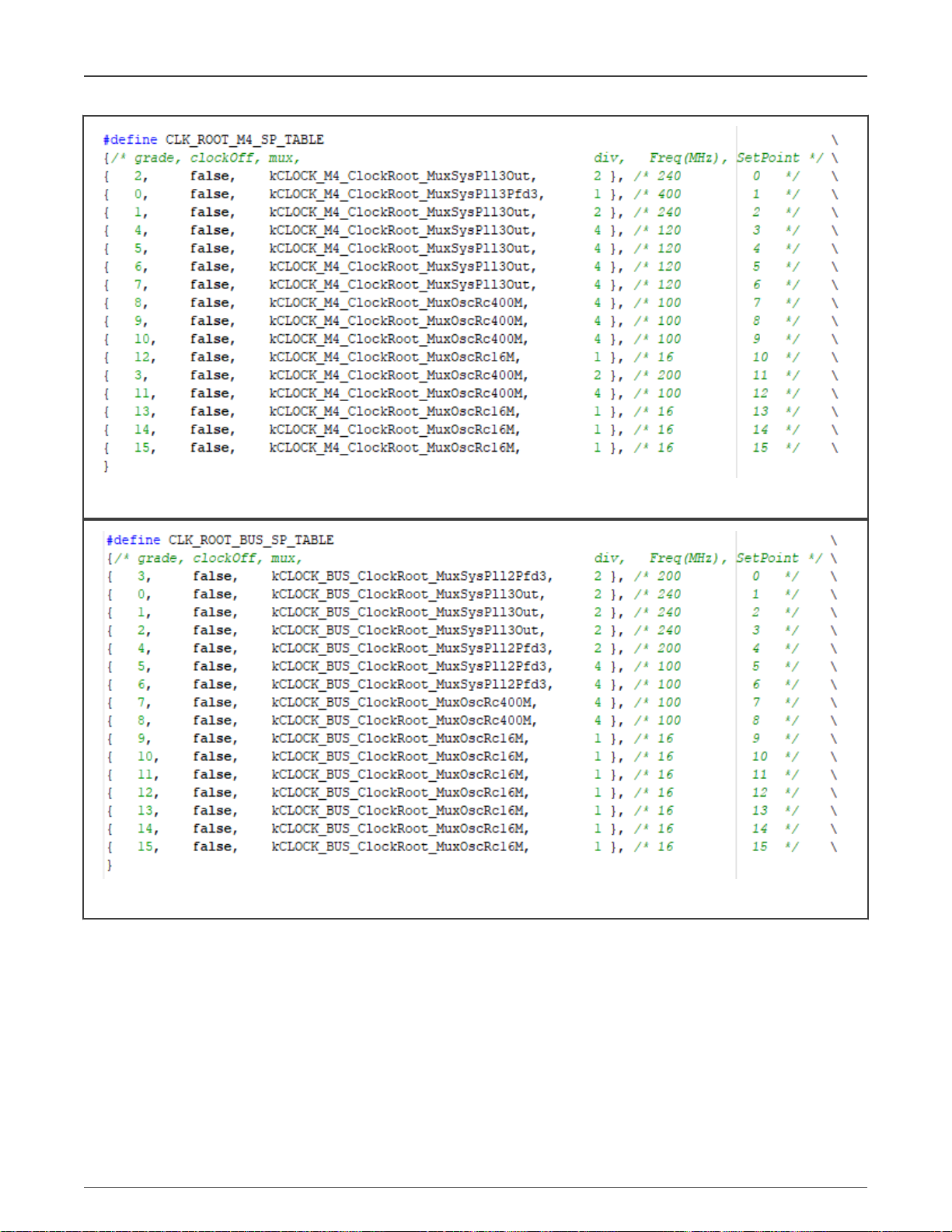
NXP Semiconductors
Figure 11. CLK_ROOT_M4_SP_TABLE macro
Creating low-power mode configuration
Figure 12. CLOCK_ROOT_BUS_SP_TABLE macro
I.MXRT1170 Low-Power Modes, Rev. 0, 03/2021
Application Note 42 / 59
Page 43

NXP Semiconductors
Figure 13. CLOCK_ROOT_BUS_LPSR_SP_TABLE macro
Creating low-power mode configuration
There is another configuration macro which determines the clock root control settings. Figure 14 shows part of
the CLK_ROOT_CONFIGURATION_TABLE macro. If the UNASSIGNED, CM7_DOMAIN, or CM4_DOMAIN control
mode is selected, the default clock root clock settings are used and they can be changed by software using the
CLOCK_ROOTn_CONTROL register. The difference between the UNASSIGNED and DOMAIN control modes is that in the
DOMAIN control mode, only the selected domain can change the clock root clock settings.
Figure 14. CLK_ROOT_CONFIGURATION_TABLE macro
Table 36. Power mode switch example CCM clock root configuration functions
Called functions Description
CLOCK_ROOT_ControlBySetPointMode Enables the Setpoint mode and applies the configured setpoint settings
CLOCK_ROOT_ControlByDomainMode
I.MXRT1170 Low-Power Modes, Rev. 0, 03/2021
Application Note 43 / 59
Enables the Domain mode and assigns the selected domain to the
WHITE_LIST field
Page 44

NXP Semiconductors
Creating low-power mode configuration
Figure 15. CCM clock root configuration
1. If SP_CTRL is selected in the CLK_ROOT_CONFIGURATION_TABLE macro, this block of code is
used to configure the required settings. According to the CLOCK_ROOT_X_SP_TABLE macro, the
CLOCK_ROOT_ControlBySetPointMode
function configures the appropriate clock root. If the Setpoint control mode
is required for another clock root, another case must be added into this switch block.
2. If CM7_DOMAIN or CM4_DOMAIN is selected in the CLK_ROOT_CONFIGURATION_TABLE macro, this block is used
to configure the required settings. In this case, the clock root clock settings remain in the default state and if a change
is required, this must be done by software. See Figure 15 for the clock root configuration example, which selects PLL3/2
as a source clock, sets the divider to 1, and enables the clock root clock output.
I.MXRT1170 Low-Power Modes, Rev. 0, 03/2021
Application Note 44 / 59
Page 45

NXP Semiconductors
Creating low-power mode configuration
Figure 16. GPT1 clock root configuration
Table 37 shows the CCM clock roots initialization provided by the power mode switch example.
Table 37. Power mode switch example CCM Clock root configuration
CM7 clock root CM4 clock root BUS clock root BUS_LPSR clock root
0 ARM_PLL PLL3/2 PLL2_PFD3/2 PLL3/4
1 SYS_PLL1 PLL3_PFD3/1 PLL3/2 PLL3/3
2 SYS_PLL1 PLL3/2 PLL3/2 PLL3/4
3 SYS_PLL1 PLL3/4 PLL3/2 PLL3/8
4 ARM_PLL PLL3/4 PLL2_PFD3/2 PLL3/8
5 SYS_PLL3/2 PLL3/4 PLL2_PFD3/4 PLL3/8
6 SYS_PLL3/2 PLL3/4 PLL2_PFD3/4 PLL3/8
7 RC400/2 RC400/4 RC400/4 RC400/8
8 RC_400M/2 RC400/4 RC400/4 RC400/8
9 RC_16M RC400/4 RC_16M RC400/8
10 RC_16M RC_16M RC_16M RC_16M
11 RC_16M RC400/2 RC_16M RC400/4
12 RC_16M RC400/4 RC_16M RC400/8
13 RC_16M RC_16M RC_16M RC_16M
14 RC_16M RC_16M RC_16M RC_16M
15 RC_16M RC_16M RC_16M RC_16M
5.5.2 Clock sources configuration
As mentioned in Clock sources (OSCPLLs), the clock sources support four types of control. The
CLK_OSCPLL_CONFIGURATION_TABLE macro is defined in
configuration. See Figure 17.
I.MXRT1170 Low-Power Modes, Rev. 0, 03/2021
Application Note 45 / 59
chip_init_config.h
, which determines the clock sources
Page 46
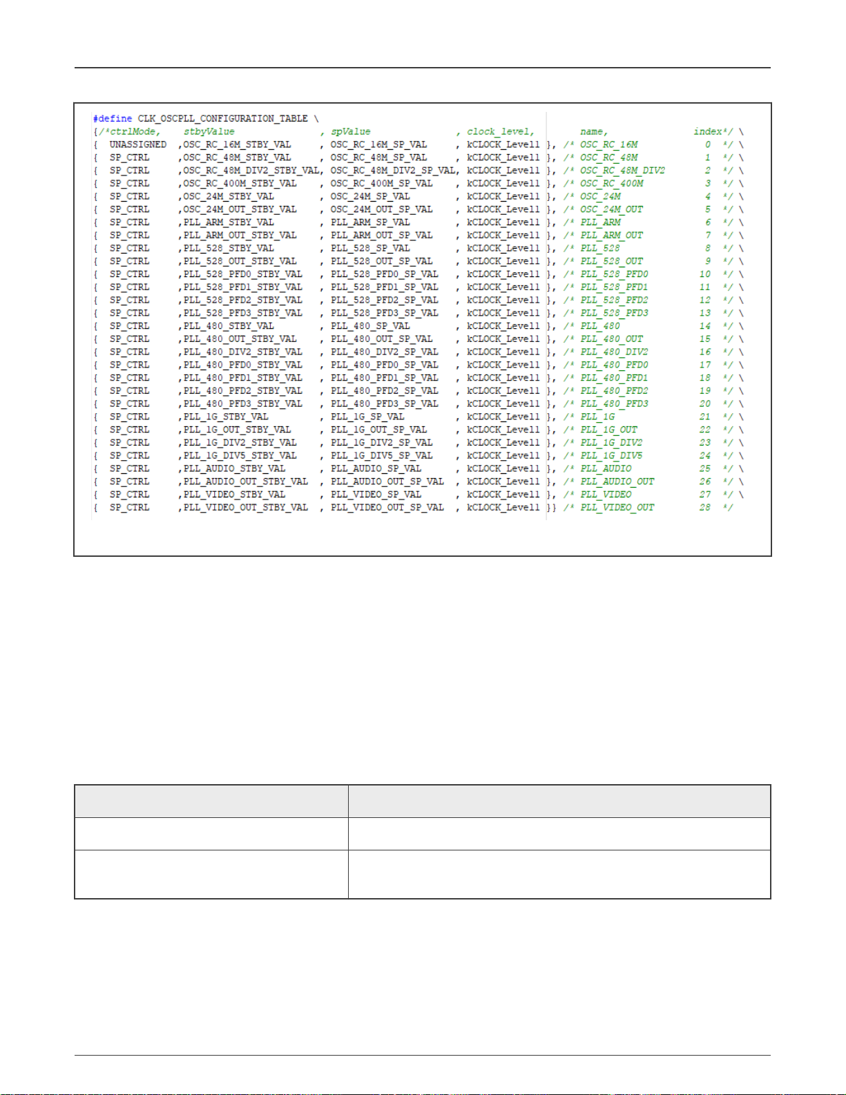
NXP Semiconductors
Creating low-power mode configuration
Figure 17. CLK_OSCPLL_CONFIGURATION_TABLE macro
• The first column of the CLK_OSCPLL_CONFIGURATION_TABLE macro determines the control mode used. It is possible
to configure the UNASSIGNED mode, the SP_CTRL mode, and the CM7_CTRL or CM4_CTRL control modes (CPULPM
mode).
• The second column determines if the clock source is enabled or disabled when the MCU enters system Standby. This
column‘s settings are applied only if the SP_CTRL mode is selected for the appropriate clock source.
• The third column determines in which setpoint the clock source is enabled or disabled. This column’s settings are applied
only if the SP_CTRL mode is selected for the appropriate clock source.
• The fourth column determines if the clock source is enabled or disabled in a certain CPU mode (Run, Wait, Stop, and
Suspend). This column‘s settings are applied only if the CM7_CTRL or CM4_CTRL mode is selected for the appropriate
clock source.
Table 38. Power mode switch example CCM clock root configuration functions
Called functions Description
CLOCK_OSCPLL_ControlBySetPointMode Enables the Setpoint mode and applies the configured setpoint settings
CLOCK_OSCPLL_ControlByCpuLowPowerModeEnables the CPULPM mode, assigns the domain to the WHITE_LIST field,
and sets the domain level
I.MXRT1170 Low-Power Modes, Rev. 0, 03/2021
Application Note 46 / 59
Page 47
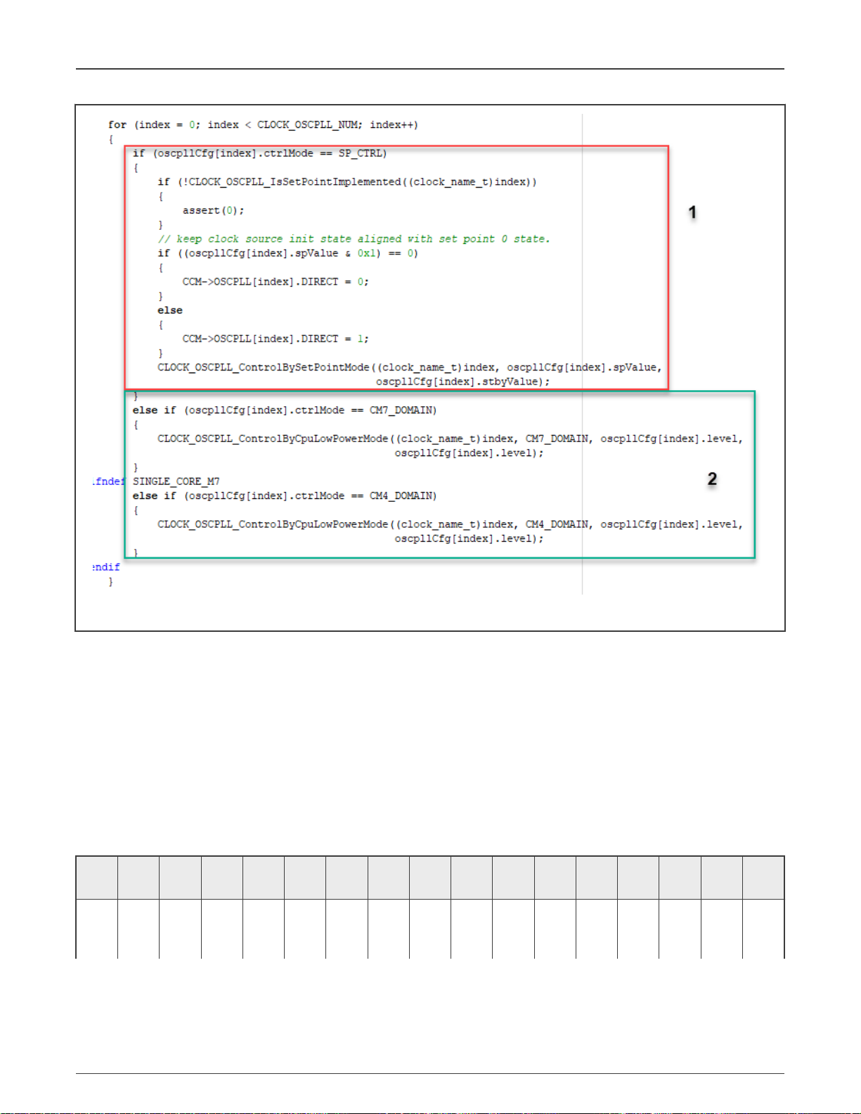
NXP Semiconductors
Creating low-power mode configuration
Figure 18. CCM Clock sources configuration
1. If SP_CTRL is selected in the CLK_OSCPLL_CONFIGURATION_TABLE macro, this block of code configures the
required settings. Before the setpoint mode control is applied, the function keeps the clock sources’ initialization
state aligned with the setpoint 0 state. This if/else block is optional. The
CLOCK_OSCPLL_ControlBySetPointMode
function configures the clock sources for all setpoints according to the CLK_OSCPLL_CONFIGURATION_TABLE macro
settings.
2. If CM7_CTRL or CM4_CTRL is selected in the CLK_OSCPLL_CONFIGURATION_TABLE macro, this block is used
to configure the required settings. The
CLOCK_OSCPLL_ControlByCpuLowPowerMode
function configures the clock
source settings according to the CLK_OSCPLL_CONFIGURATION_TABLE macro.
Table 39 shows the CCM clock sources initialization provided by the power mode switch example. The "+" symbol means that the
clock source is enabled in the selected setpoint. The "-" symbol means that the clock source is disabled in the selected setpoint.
Table 39. Power mode switch example CCM Clock sources configuration visualization
Setp
0 1 2 3 4 5 6 7 8 9 10 11 12 13 14 15
oint
OSC
+ + + + + + + + + + + + + + + +
_RC_
16M
Table continues on the next page...
I.MXRT1170 Low-Power Modes, Rev. 0, 03/2021
Application Note 47 / 59
Page 48

NXP Semiconductors
Creating low-power mode configuration
Table 39. Power mode switch example CCM Clock sources configuration visualization (continued)
Setp
0 1 2 3 4 5 6 7 8 9 10 11 12 13 14 15
oint
OSC
- - - - - - - - - - - - - - - _RC_
48M
OSC
- - - - - - - - - - - - - - - _RC_
48M_
DIV2
OSC
+ + + + + + + + + + + + + + +
_RC_
400M
OSC
+ + + + + + + - - - - - - - - _24M
OSC
+ + + + + + + - - - - - - - - _24M
_CLK
ARM
+ + + + + - - - - - - - - - - _PLL
ARM
+ + + + + - - - - - - - - - - _PLL
_CLK
SYS_
+ + + + + + + - - - - - - - - PLL2
SYS_
+ + + + + + + - - - - - - - - PLL2
_CLK
SYS_
+ + + + + + + - - - - - - - - PLL2
_PFD
0
SYS_
+ + + + + + + - - - - - - - - PLL2
_PFD
1
SYS_
+ + + + + + + - - - - - - - - PLL2
_PFD
2
SYS_
+ + + + + + + - - - - - - - - PLL2
_PFD
3
Table continues on the next page...
I.MXRT1170 Low-Power Modes, Rev. 0, 03/2021
Application Note 48 / 59
Page 49

NXP Semiconductors
Creating low-power mode configuration
Table 39. Power mode switch example CCM Clock sources configuration visualization (continued)
Setp
0 1 2 3 4 5 6 7 8 9 10 11 12 13 14 15
oint
SYS_
+ + + + + + + - - - - - - - - PLL3
SYS_
+ + + + + + + - - - - - - - - PLL3
_OU
T
SYS_
+ + + + + + + - - - - - - - - PLL3
_DIV
2
SYS_
+ + + + + + + - - - - - - - - PLL3
_PFD
0
SYS_
+ + + + + + + - - - - - - - - PLL3
_PFD
1
SYS_
+ + + + + + + - - - - - - - - PLL3
_PFD
2
SYS_
+ + + + + + + - - - - - - - - PLL3
_PFD
3
SYS_
- + + + - - - - - - - - - - - -
PLL1
SYS_
- + + + - - - - - - - - - - - PLL1
_CLK
SYS_
- + + + - - - - - - - - - - - PLL1
_DIV
2
SYS_
- + + + - - - - - - - - - - - PLL1
_DIV
5
AUDI
+ + + + + + + - - - - - - - - O_PL
L
Table continues on the next page...
I.MXRT1170 Low-Power Modes, Rev. 0, 03/2021
Application Note 49 / 59
Page 50

NXP Semiconductors
Creating low-power mode configuration
Table 39. Power mode switch example CCM Clock sources configuration visualization (continued)
Setp
0 1 2 3 4 5 6 7 8 9 10 11 12 13 14 15
oint
AUDI
+ + + + + + + - - - - - - - - O_PL
L_CL
K
VIDE
+ + + + + + + - - - - - - - - O_PL
L
VIDE
+ + + + + + + - - - - - - - - O_PL
L_CL
K
When the system standby is entered, all clock sources are disabled in the Power mode switch example. See
setpoint_table_def.h
and find the section with the Clock sources STBY_VAL values, for example #define OSC_RC_16M_STBY_VAL.
5.5.3 Module clocks configuration
As mentioned in Module clocks (LPCGs), the module clocks support four types of control. The
CLK_LPCG_CONFIGURATION_TABLE macro is defined in
configuration. Because there are 137 module clocks defined in the macro, the figure below shows only a few module clocks
settings. Table 11 contains the list of module clocks supported by the Setpoint control mode. The module clocks, which do not
support the Setpoint control mode, can be controlled by the CPU state or they can be UNASSIGNED.
chip_init_config.h
, which determines the module clocks
I.MXRT1170 Low-Power Modes, Rev. 0, 03/2021
Application Note 50 / 59
Page 51

NXP Semiconductors
Creating low-power mode configuration
• The first column of the CLK_LPCG_CONFIGURATION_TABLE macro is used to determine what control mode is used for
the appropriate module clock. CM7_DOMAIN or CM4_DOMAIN can be used for every module clock, SP_CTRL is only
supported by some of the module clocks.
• The second column determines if the module clock is enabled or disabled when the MCU enters the system Standby. This
column is defined only when the module clock supports the Setpoint control mode. This column‘s settings are applied only
if the SP_CTRL mode is selected for the appropriate clock source.
• The third column determines in which setpoint the module clock is enabled or disabled. This column is defined only when
the module clock supports the Setpoint control mode. This column’s settings are applied only if the SP_CTRL mode is
selected for the appropriate clock source.
• The fourth column determines if the module clock is enabled or disabled in a certain CPU mode (Run, Wait, Stop,
and Suspend). This column’s settings are applied only if the CM7_DOMAIN or CM4_DOMAIN mode is selected for the
appropriate module clock.
Table 40. Power mode switch example CCM module clocks configuration functions
Called functions Description
CLOCK_LPCG_ControlBySetPointMode Enables the Setpoint mode and applies the configured setpoint settings
Table continues on the next page...
I.MXRT1170 Low-Power Modes, Rev. 0, 03/2021
Application Note 51 / 59
Page 52

NXP Semiconductors
Creating low-power mode configuration
Table 40. Power mode switch example CCM module clocks configuration functions (continued)
Called functions Description
CLOCK_LPCG_ControlByCpuLowPowerModeEnables the CPULPM mode, assigns the domain to the WHITE_LIST field, and
sets the domain level
Figure 19. CCM module clocks configuration
1. If SP_CTRL is selected in the CLK_LPCG_CONFIGURATION_TABLE macro, this block of code configures the required
settings. The
CLOCK_LPCG_ControlBySetPointMode
function configures the module clocks for all setpoints according
to the CLK_LPCG_CONFIGURATION_TABLE macro settings.
2. If CM7_DOMAIN or CM4_DOMAIN is selected in the CLK_LPCG_CONFIGURATION_TABLE macro, this block
configures the required settings. The
CLOCK_LPCG_ControlByCpuLowPowerMode
function configures the module
clocks settings according to the CLK_LPCG_CONFIGURATION_TABLE macro.
The visualization table for the module clocks is not included in the document, because it is too long. The same rules are applied
for the module clocks’ settings, as described in Clock sources configuration. The visualization table can be easily built according
to these rules.
5.5.4 CCM configuration tips
• It is recommended to start the configuration with the clock sources, because all other CCM settings are dependent on the
clock sources.
• OSC_24M and OSC_24M_CLK are tied together. OSC_24M_CLK is the output of OSC_24M. If OSC_24M is disabled,
OSC_24M_CLK cannot be used. The same settings should be used for both clock sources.
• The same situation as that described above can be applied for the PLL settings. If the PLL clock is disabled, the PLL_PFD
clock must be disabled too.
• When the clock source is disabled in a certain setpoint or CPU state, this clock source must not be used as a source clock
for any clock root. Always check which clock sources are enabled and only these can be used in the clock roots in the
appropriate setpoints or CPU states.
• During CLK_LPCG_CONFIGURATION_TABLE definition, it is necessary to check if the appropriate clock root is enabled.
If the appropriate clock root is disabled, the module clock must be disabled too.
I.MXRT1170 Low-Power Modes, Rev. 0, 03/2021
Application Note 52 / 59
Page 53

NXP Semiconductors
Creating low-power mode configuration
• Not all module clocks can be disabled for correct MCU functionality.
5.6 PMU_InitConfig()
PMU_InitConfig is used to configure settings like LDOs and body bias. This function is based on a set of configuration macros and
functions which provides the required settings. All configuration macros are placed in
of the macros defined for the PMU.
setpoint_table_def.h
. Figure 20 lists some
Figure 20. PMU configuration macros
Table 41. Power mode switch example PMU configuration functions
Called functions Allowed modules Description
kPMU_FBB_CM7,
PMU_GPCEnableBodyBias
kPMU_RBB_SOC,
kPMU_RBB_LPSR
kPMU_PllLdo,
PMU_GPCEnableLdo
kPMU_LpsrAnaLdo,
kPMU_LpsrDigLdo
PMU_GPCSetLdoOperateMode
PMU_GPCEnableLdoTrackingM
ode
kPMU_LpsrAnaLdo,
kPMU_LpsrDigLdo
kPMU_LpsrAnaLdo,
kPMU_LpsrDigLdo
PMU_GPCEnableLdoBypassModekPMU_LpsrAnaLdo,
kPMU_LpsrDigLdo
Enables or disables the selected body bias according to the provided
setpoint map
Enables or disables the selected LDO according to the provided
setpoint map
Selects the LDO operate mode according to the provided
setpoint map
Enables or disables the Tracking mode for a selected LDO according
to the provided setpoint map
Enables or disables the Bypass mode for a selected LDO according
to the provided setpoint map
Table continues on the next page...
I.MXRT1170 Low-Power Modes, Rev. 0, 03/2021
Application Note 53 / 59
Page 54

NXP Semiconductors
Table 41. Power mode switch example PMU configuration functions (continued)
Creating low-power mode configuration
PMU_GPCEnableBandgap
PMU_GPCEnableBodyBiasStan
dbyMode
PMU_GPCEnableLdoStandbyM
ode
PMU_GPCEnableBandgapStan
dbyMode
PMU_GPCSetLpsrDigLdoTarge
tVoltage
PMU_SetLpsrDigLdoControlMo
de
PMU_SetLpsrAnaLdoControlMo
de
PMU_SetPllLdoControlMode
kPMU_FBB_CM7,
kPMU_RBB_SOC,
kPMU_RBB_LPSR
kPMU_PllLdo,
kPMU_LpsrAnaLdo,
kPMU_LpsrDigLdo
Enables or disables the PMU Bandgap according to the provided
setpoint map
Enables or disables the selected body bias when the System standby
is active according to the provided setpoint map
Enables or disables the selected LDO when the System standby is
active according to the provided setpoint map
Enables or disables the PMU Bandgap when the System standby is
active according to the provided setpoint map
Sets the Dig LDO target output voltage according to the
provided configuration
Selects between the software and hardware control modes
PMU_SetBandgapControlMode
kPMU_FBB_CM7,
PMU_SetBodyBiasControlMode
kPMU_RBB_SOC,
kPMU_RBB_LPSR
After the power-on reset, the body bias control and all LDOs’ control is set to the software control mode. The body bias is disabled
by default and all LDOs are enabled after power on reset.
The figure below shows the steps of the PMU configuration used in the Power mode switch example.
1. Select in which setpoints are the FBB and RBB enabled. Note that the FBB and RBB cannot be enabled together in one
setpoint.
2. Enable the required LDOs and the related LDO features for all setpoints.
3. Select in which setpoints are the FBB, RBB, and LDOs enabled when the system standby is active.
4. Adjust the Dig LDO output voltage in all setpoints.
5. Switch all PMU modules into the hardware control mode.
I.MXRT1170 Low-Power Modes, Rev. 0, 03/2021
Application Note 54 / 59
Page 55

NXP Semiconductors
Creating low-power mode configuration
Figure 21. PMU configuration
Table 42. Power mode switch example PMU configuration visualization
Setp
0 1 2 3 4 5 6 7 8 9 10 11 12 13 14 15
oint
BG + + + + + + + + + + + + + + + +
FBB - + - - - - - - - - - - - - - -
FBB_
- - - - - - - - - - - - - - - STB
Y
RBB_
- - - - - - - - + - + - - - - SOC
Table continues on the next page...
I.MXRT1170 Low-Power Modes, Rev. 0, 03/2021
Application Note 55 / 59
Page 56

NXP Semiconductors
Table 42. Power mode switch example PMU configuration visualization (continued)
Setp
0 1 2 3 4 5 6 7 8 9 10 11 12 13 14 15
oint
_LPS
R
RBB_
- - - - - - - - - - - - - - - +
LPS
R
LDO_
+ + + + + + - - - - - - - - - EN_P
LL
LDO_
- - - - - - - - - - - + + + + +
ANA_
EN
LDO_
- - - - - - - - - - - - - - - ANA_
LP_M
ODE
Creating low-power mode configuration
LDO_
- - - - - - - - - - - + + + + +
ANA_
TRA
CKIN
G_E
N
LDO_
- - - - - - - - - - - + + + + +
ANA_
BYP
ASS_
EN
LDO_
+ + - + + - + + + + - + + + +
DIG_
EN
LDO_
- - - - - - - - - - - - - - - DIG_
LP_M
ODE
LDO_
+ + - - + + - + + + + - + + + +
DIG_
TRA
CKIN
G_E
N
LDO_
+ + - - + + - + + + + - + + + +
DIG_
BYP
Table continues on the next page...
I.MXRT1170 Low-Power Modes, Rev. 0, 03/2021
Application Note 56 / 59
Page 57

NXP Semiconductors
Table 42. Power mode switch example PMU configuration visualization (continued)
Setp
0 1 2 3 4 5 6 7 8 9 10 11 12 13 14 15
oint
ASS_
EN
BG_
- - - - - - - - - - - - - - - STB
Y
FBB_
- - - - - - - - - - - - - - - STB
Y
RBB_
- - - - - - - - - - - - - - - SOC
_LPS
R_ST
BY
RBB_
- - - - - - - - - - - - - - - LPS
R_ST
BY
Creating low-power mode configuration
LDO_
- - - - - - - - - - - - - - - PLL_
EN_S
TBY
LDO_
- - - - - - - - - - - - - - - ANA_
EN_S
TBY
(HP/L
P
mode
)
LDO_
- - - - - - - - - - - - - - - DIG_
EN_S
TBY
(HP/L
P
mode
)
The "+" symbol signalizes that the feature is enabled in the selected setpoint. The "-" symbol signalizes that the feature is disabled
in the selected setpoint.
The "+" symbol signalizes that the LDO ANA and LDO DIG are in the low-power mode when the system standby is entered.
The "-" symbol signalizes that the LDO ANA and LDO DIG are in the high-power mode when the system standby is entered. This
is applicable to the last two lines of the table.
I.MXRT1170 Low-Power Modes, Rev. 0, 03/2021
Application Note 57 / 59
Page 58

NXP Semiconductors
Setpoint and CPU mode transition
5.6.1 PMU configuration tips
• When the FBB is enabled in a certain setpoint, the RBB must be always disabled in the same setpoint. Always ensure that
the FBB and RBB are not enabled together in the same setpoint.
• If 1 GHz without ECC or 800 MHz with ECC is the required frequency for the M7 core, the FBB must be enabled.
• The PLL LDO must be enabled in the setpoints that use any PLLs. If no PLLs are used, the PLL LDO can be disabled.
• The ANA LDO must be enabled in all setpoints where the DCDC is disabled. In this case, only the LPSR domain is
powered.
• The ANA LDO can be enabled even if the DCDC is enabled in the same setpoint. This configuration makes sense when
different VDD1P8 voltages are required for the SoC and LPSR power domains.
• The DIG LDO must be enabled in all setpoints where the DCDC or DCDC_DIG are disabled.
• The DIG LDO can be enabled even if the DCDC is enabled in the same setpoint. This configuration makes sense when
different VDD1P0 voltages are required for the SoC and LPSR power domains.
• When the ANA LDO and DIG LDO tracking is enabled, force the low-power mode to disable. The tracking enable should
happen before the bypass enable and the tracking disable should happen after the bypass disable. See chapter 17.3.2
Control Mode in the Reference Manual for all information about the LDO and body bias settings.
6 Setpoint and CPU mode transition
The
PowerModeTransition
GPC_CM_RequestSleepModeSetPointTransition
There are five parameters required by the function.
1. cpuMode – The CPU mode that the core transitions to.
2. sleepSP - The setpoint that the CPU wants the system to transit to in the next CPU platform sleep sequence.
3. wakeupSP - The setpoint that the CPU wants the system to transit to in the next CPU platform wakeup sequence.
4. wakeupSel - 0: the system goes to the “wakeupSp” setpoint.
1: the system goes back to the setpoint before entering the low-power mode.
5. stbyEn - true means that a standby request is asserted to the GPC when the CPU enters the low-power mode.
See functions
of how the setpoint transition and the CPU mode change can be implemented. Note that the
switches between the setpoints and CPU modes already defined in the example code. When a custom setpoint configuration is
created or when other than the default setpoints are used, the
For all supported setpoints transitions, run the Power mode switch example code.
TypicalSetPointTransition
function is implemented in
and
and
CpuModeSwitchInSetPoint
lpm.c
for the setpoint transition and CPU mode change. This function calls
CpuModeTransition
, which execute a complete mode transition.
in the Power mode switch example for a basic overview
TypicalSetPointTransition
TypicalSetPointTransition
function must be updated.
function
I.MXRT1170 Low-Power Modes, Rev. 0, 03/2021
Application Note 58 / 59
Page 59

How To Reach Us
Home Page:
nxp.com
Web Support:
nxp.com/support
Information in this document is provided solely to enable system and software implementers to use NXP products. There
are no express or implied copyright licenses granted hereunder to design or fabricate any integrated circuits based on the
information in this document. NXP reserves the right to make changes without further notice to any products herein.
NXP makes no warranty, representation, or guarantee regarding the suitability of its products for any particular purpose, nor
does NXP assume any liability arising out of the application or use of any product or circuit, and specifically disclaims any
and all liability, including without limitation consequential or incidental damages. “Typical” parameters that may be provided
in NXP data sheets and/or specifications can and do vary in different applications, and actual performance may vary over
time. All operating parameters, including “typicals,” must be validated for each customer application by customer's technical
experts. NXP does not convey any license under its patent rights nor the rights of others. NXP sells products pursuant to
standard terms and conditions of sale, which can be found at the following address: nxp.com/SalesTermsandConditions.
Right to make changes - NXP Semiconductors reserves the right to make changes to information published in this
document, including without limitation specifications and product descriptions, at any time and without notice. This
document supersedes and replaces all information supplied prior to the publication hereof.
Security — Customer understands that all NXP products may be subject to unidentified or documented vulnerabilities.
Customer is responsible for the design and operation of its applications and products throughout their lifecycles to reduce
the effect of these vulnerabilities on customer’s applications and products. Customer’s responsibility also extends to other
open and/or proprietary technologies supported by NXP products for use in customer’s applications. NXP accepts no
liability for any vulnerability. Customer should regularly check security updates from NXP and follow up appropriately.
Customer shall select products with security features that best meet rules, regulations, and standards of the intended
application and make the ultimate design decisions regarding its products and is solely responsible for compliance with all
legal, regulatory, and security related requirements concerning its products, regardless of any information or support that
may be provided by NXP. NXP has a Product Security Incident Response Team (PSIRT) (reachable at PSIRT@nxp.com)
that manages the investigation, reporting, and solution release to security vulnerabilities of NXP products.
NXP, the NXP logo, NXP SECURE CONNECTIONS FOR A SMARTER WORLD, COOLFLUX,EMBRACE, GREENCHIP,
HITAG, ICODE, JCOP, LIFE, VIBES, MIFARE, MIFARE CLASSIC, MIFARE DESFire, MIFARE PLUS, MIFARE FLEX,
MANTIS, MIFARE ULTRALIGHT, MIFARE4MOBILE, MIGLO, NTAG, ROADLINK, SMARTLX, SMARTMX, STARPLUG,
TOPFET, TRENCHMOS, UCODE, Freescale, the Freescale logo, AltiVec, CodeWarrior, ColdFire, ColdFire+, the Energy
Efficient Solutions logo, Kinetis, Layerscape, MagniV, mobileGT, PEG, PowerQUICC, Processor Expert, QorIQ, QorIQ
Qonverge, SafeAssure, the SafeAssure logo, StarCore, Symphony, VortiQa, Vybrid, Airfast, BeeKit, BeeStack, CoreNet,
Flexis, MXC, Platform in a Package, QUICC Engine, Tower, TurboLink, EdgeScale, EdgeLock, eIQ, and Immersive3D are
trademarks of NXP B.V. All other product or service names are the property of their respective owners. AMBA, Arm, Arm7,
Arm7TDMI, Arm9, Arm11, Artisan, big.LITTLE, Cordio, CoreLink, CoreSight, Cortex, DesignStart, DynamIQ, Jazelle,
Keil, Mali, Mbed, Mbed Enabled, NEON, POP, RealView, SecurCore, Socrates, Thumb, TrustZone, ULINK, ULINK2,
ULINK-ME, ULINK-PLUS, ULINKpro, μVision, Versatile are trademarks or registered trademarks of Arm Limited (or its
subsidiaries) in the US and/or elsewhere. The related technology may be protected by any or all of patents, copyrights,
designs and trade secrets. All rights reserved. Oracle and Java are registered trademarks of Oracle and/or its affiliates. The
Power Architecture and Power.org word marks and the Power and Power.org logos and related marks are trademarks and
service marks licensed by Power.org.
©
NXP B.V. 2021. All rights reserved.
For more information, please visit: http://www.nxp.com
For sales office addresses, please send an email to: salesaddresses@nxp.com
Date of release: 03/2021
Document identifier: AN13148
 Loading...