

Page 1

AN13133
Secure JTAG for i.MXRT1170
Rev. 0 — 02/2021
by: NXP Semiconductors
Contents
1 Introduction
This document describes how the Secure JTAG on the i.MX RT1170 MCU
family can be used.
The i.MX RT series JTAG Controller (JTAGC) provides a possibility to regulate
the JTAG access. The three JTAG security modes are available in the i.MX
RT series:
• No Debug mode—Maximum security is provided in this mode. All
security-sensitive JTAG features are permanently blocked, preventing any debug.
• Secure JTAG mode—High security is provided in this mode. Secret key-based challenge/response authentication
mechanism is used for JTAG access
• JTAG Enabled mode—Low security is provided in this mode. It is the default mode of operation for the JTAGC.
Moreover, you can also fully disable the JTAGC functionality. For configuration of these JTAG modes, One Time Programmable
(OTP) eFuses are used and burned after packaging. The fuse burning process is irreversible. It is impossible to revert the fuse
back to the unburned state. To explain, Secure JTAG mode is used in this document. The aim is to allow return/field testing.
Authorized reactivation of the JTAG port is allowed in this mode.
1 Introduction......................................1
2 i.MX RT1170 Secure JTAG support
........................................................ 1
3 Secret response key approaches....6
4 Debugging with the Secure JTAG
enabled............................................7
5 Conclusion.....................................10
6 References....................................11
Application Note
There are several hardware modifications that must be made to fully enable the JTAG on an RT1170-EVK. The resistors R37,
R41, R42, R43, and R44 must to be soldered on. The resistors R78, R187, R195, and R208 must be removed. See the hardware
design manual and the EVKB schematic for more details.
Before the Secure JTAG can be enabled, enable also the HAB and set it to the HAB Closed mode. You can find the step-by-step
guide for enabling HAB in the i.MX RT1170 security application note.
2 i.MX RT1170 Secure JTAG support
JTAG access is limited in the Secure JTAG mode by using a challenge/response-based authentication. Any access to JTAG port is
internally checked. Only the devices authorized for debugging (with the right response) can access the JTAG port, otherwise JTAG
access is denied. The external debugger tools (such as SEGGER J-Link, Lauterbach Trace32, Arm RVDS/DS5, etc.) supporting
the challenge/response-based authentication mechanism can be used. The secure JTAG mode is typically enabled in the factory
manufacturing and not used during the development.
2.1 How to put the chip in Secure JTAG mode
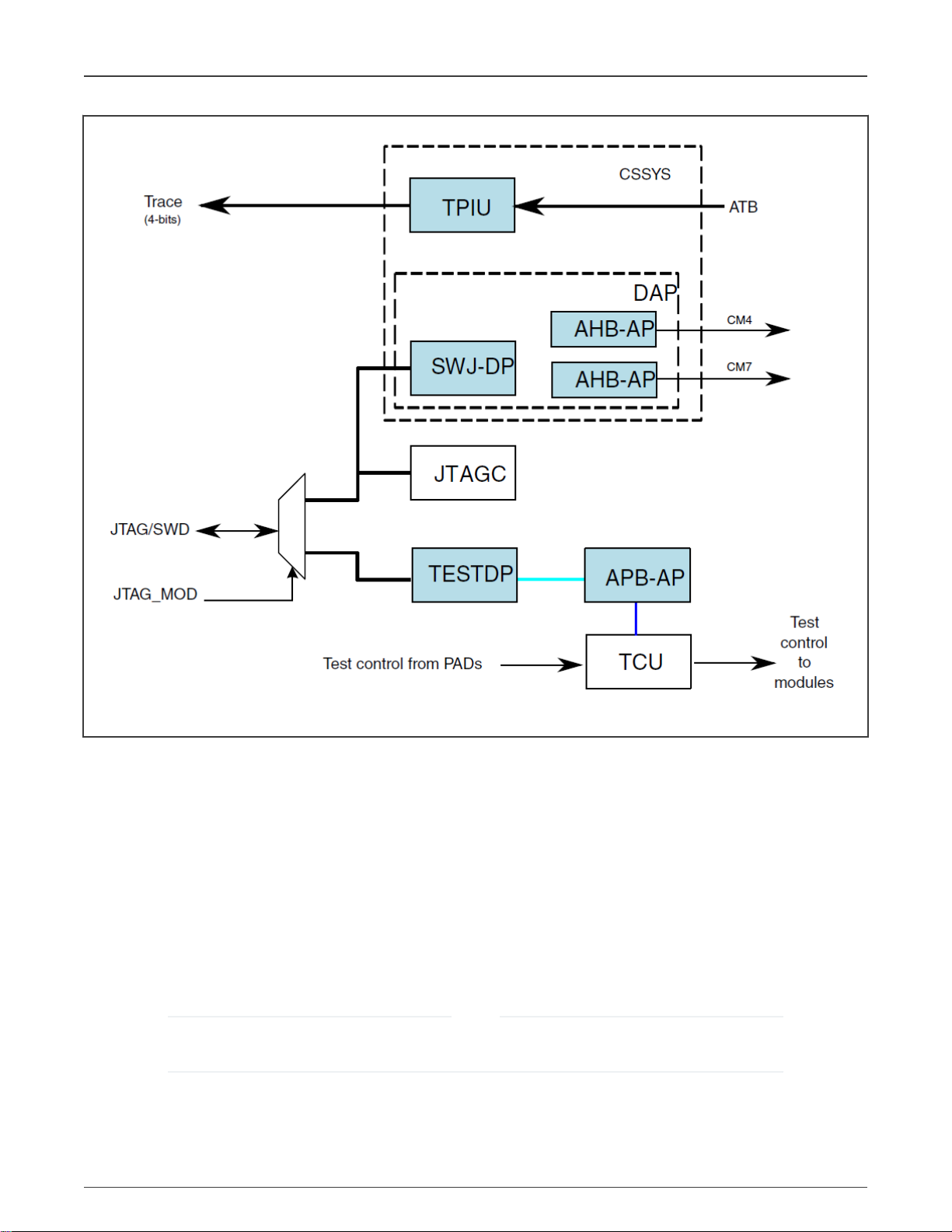
There is only one JTAG interface on the chip with two JTAG modes. The modes can be switched via the JTAG_MOD signal
(GPIO_LPSR_13 Alt0). When JTAG_MOD is in log. 0, the JTAG interface is in the debug mode and the DAP and JTAGC are
enabled. When JTAG_MOD is in log. 1, the JTAG interface is in the test mode and only TESTDP is enabled. For more information,
see the
Chip and Arm Platform Debug Architecture
chapter in the reference manual.
Page 2
NXP Semiconductors
i.MX RT1170 Secure JTAG support
Figure 1. System Level Debug Architecture
2.2 i.MX RT JTAGC security modes
The i.MX RT1170 JTAG Controller (JTAGC) supports three different security modes. JTAG enabled is the default mode of
operation for JTAGC. The user can select the Secure JTAG mode by programing a value 0x1 to the eFuse labeled JTAG_SMODE,
described in Table 1. The eFuse has the default value 0x0, which means that the JTAG controller is unsecured by default.
Further details on eFuses are available in the Fusemap and On-Chip OTP Controller (OCOTP_CTRL) chapters in the appropriate
SRM_RT1170 Security Reference Manual for the i.MX RT1170 available at www.nxp.com upon a request.
To lock a specific fuse word and prevent further modifications to all the fuses inside the fuse word, set the WORDLOCK bit of the
OCOTP register to 0x1 before writing into one of the fuses inside the chosen word. When the writing operation is completed, the
whole word is prevented from changing forever.
For more information, see the
(document IMXRT1170RM).
Programming these fuses disables access to functions and JTAG Security Mode fuse bits. Users should ensure
that it is programmed last, once the final fuse configuration has been decided.
Bank redundancy vs ECC
and
Lock Bits
NOTE
chapters of the
i.MX RT1170 Processor Reference Manual
Secure JTAG for i.MXRT1170, Rev. 0, 02/2021
Application Note 2 / 12
Page 3

NXP Semiconductors
i.MX RT1170 Secure JTAG support
Table 1. eFuses associated with the Secure JTAG feature
Addr[bits] Fuse Name Fuse Function Settings
0x960[9] JTAG_HEO
0x960[1] SEC_CONFIG[1]
0x960[7:6] JTAG_SMODE[1:0]
JTAG HAB Enable Override.
Disallows HAB JTAG
enabling. The HAB may
normally enable JTAG
debugging by means of
the HAB_JDE-bit in the
OCOTP SCS register. The
JTAG_HEO-bit can override
this behavior
Security Configuration
Mode (together
with SEC_CONFIG[0])
JTAG Security Mode. Controls
the security mode of the JTAG
debug interface
0 - HAB may enable JTAG
debug access 1 - HAB
JTAG enable is overridden
(HAB may not enable JTAG
debug access)
SEC_CONFIG[1:0]:
00 - FAB (Open)
01 - Open - allows any code to
be flashed and executed, even
if it has no valid signature.
1x - Closed (Security On)
This is programmed during the
HAB enablement phase (By
setting the HAB Closed mode)
00 - JTAG enable
mode (Default)
01 - Secure JTAG mode
0x960[11] JTAG_DISABLE
0x880[14:11]
JTAG_RESP_RLOCK[3:0] JTAG_RESP_RLOCK[0]:
Table continues on the next page...
Additional JTAG mode with
the highest level of JTAG
protection, thereby overriding
the JTAG_SMODE eFuses. In
this mode all JTAG features
are disabled including Secure
JTAG and Boundary Scan
Read lock
of JTAG_RESP[31:0]
JTAG_RESP_RLOCK[1]:
Read lock
of JTAG_RESP[63:32]
JTAG_RESP_RLOCK[2]:
Read lock
of JTAG_RESP[95:64]
JTAG_RESP_RLOCK[3]:
Read lock
of JTAG_RESP[127:96]
11 - No debug mode
0 - JTAG is enabled
1 - JTAG is disabled
Read Lock
0000 - Unlock (The controlled
field can be read in the
corresponded IIM register)
1111 - Lock (The controlled
field can't be read in the
corresponded IIM register)
others - should not be set
Secure JTAG for i.MXRT1170, Rev. 0, 02/2021
Application Note 3 / 12
Page 4

NXP Semiconductors
i.MX RT1170 Secure JTAG support
Table 1. eFuses associated with the Secure JTAG feature (continued)
Addr[bits] Fuse Name Fuse Function Settings
0xCB0-0xCE0 JTAG_RESP[127:0]
Response reference value for
-
the secure JTAG controller
NOTE
The level of security cannot be reduced but only increased. Since debug modes are controlled by OTP (Hardware
fuses), bits can only be blown once.
For example, following mode changes are possible:
− “JTAG Enabled” to “Secure JTAG”
− “Secure JTAG” to “No debug”
2.3 Secure JTAG eFuses
The challenge/response mechanism used to authenticate the JTAG accesses uses a challenge value and the associated secret
response key. The keys are stored in eFuses inside the IC. The i.MX RT1170 series eFuses used to store the challenge value
and the secret response key are listed below:
• The challenge value is the “Device Unique ID” which is programmed into the eFuses. This Device ID is unique for
each IC and can be read from the OCOTP registers by their Fuse Row Index as follows: OCOTP->FUSE016 and
OCOTP->FUSE017. The eFuses are programmed during manufacturing.
• The user program the secret response key (128 bits) into the eFuses marked JTAG_RESP.
After programming the secret response key, the user must disable the ability of software running on the Arm core to read or
overwrite the response key. This is done by programming 0x1111 to the associated lock eFuse JTAG_RESP_RLOCK.
The definition of the response value is left to the user. The Arm core cannot read the value once the response fuse field is
provisioned and locked.
2.4 SW Enabled JTAG
The Secure JTAG authentication may be bypassed in SW by writing '1' to HAB_JDE (HAB JTAG DEBUG ENABLE) bit in the
e-fuse controller module. By this JTAG is opened, regardless of its security mode. The S/W JTAG enable allows JTAG enabling
without activating the challenge-Response mechanism.
The platform initialization software should set the LOCK bit for JDE bit before transferring control to the application code to ensure
that only the trusted SW can set the JDE bit.
The JTAG SW enable does not allow debug in case of boot or memory fault as it requires reset before entering debug.
The JTAG_JDE bit SW enable backdoor access can be permanently disabled by burning the JTAG_HEO fuse.
NOTE
The S/W enabled JTAG feature reduces the overall security level of the system as it relies on S/W protections. If
this feature is not required, it is strongly recommended to burn the JTAG_HEO e-fuse which disables this feature.
2.4.1 JDE bit control in HAB (High Assurance Boot)
The HAB_JDE can be set to ‘1’ by ROM boot SW after unlocking by the Authenticate CSF command.
Before generating of the signed program image, the user must edit the UNLOCK section in the .sb file and provide the device
specific UID in the proper format as a sequence of 8-bytes, see the below example for UID = 0x63e1841b440b81d2, please:
Secure JTAG for i.MXRT1170, Rev. 0, 02/2021
Application Note 4 / 12
Page 5

NXP Semiconductors
i.MX RT1170 Secure JTAG support
section (SEC_UNLOCK;
Unlock_Engine = "OCOTP",
Unlock_features = "JTAG, SCS, SRK REVOKE",
Unlock_UID = "0xe1, 0x63, 0x1b, 0x84, 0x0b, 0x44, 0xd2, 0x81"
)
For more information about the HAB_JDE SW control by platform initialization SW in HAB (High Assurance Boot) refer to section
5.2.13 Unlock (HAB only) in [5].
2.5 Secure JTAG debug authentication protocol
When the JTAGC is in the secure debug mode, the authentication process is as follows:
1. JTAG shifts the challenge key through the Test Data Output (TDO) chain.
2. On the host side, the debug tool takes the challenge key as an input and generates the expected response key.
3. The associated response key is shifted back through the Test Data Input (TDI) chain.
4. The JTAGC compares the expected internal fused response key with the one shifted in and enables the JTAG access
only if it matches.
NOTE
Any device reset after JTAG access authorization shifts the JTAG controller back to its locked state.
Figure 2 shows how the challenge/response mechanism works with the JTAG tools.
Secure JTAG for i.MXRT1170, Rev. 0, 02/2021
Application Note 5 / 12
Page 6

NXP Semiconductors
Secret response key approaches
Figure 2. Secure JTAG operation
The JTAG debug tool passes the retrieved challenge key to the user’s application and gets the associated response key in return.
The management of the challenge/response pairs is user-dependent and not handled by NXP or the debug tool vendors. Key
management is discussed further in Secret response key approaches.
2.6 JTAGC disable fuse
In addition to the various JTAG security modes implemented internally in the JTAGC, there is an option to disable the JTAGC
functionality with the JTAG_DISABLE eFuse. This eFuse creates an additional JTAG mode, JTAG Disabled with the highest level
of JTAG protection, overriding the JTAG_SMODE eFuses. In this mode all JTAG features are disabled, including Secure JTAG
and Boundary Scan; users must ensure that this fuse is not blown if they wish to use the Secure JTAG functionality.
3 Secret response key approaches
For every challenge value (“Device Unique ID” in i.MX RT1170) that is retrieved with a JTAG instruction, there is an associated
secret response key known only by the user. The JTAG tool vendor only handles the JTAG mechanism used by this authentication
process, and does not know the secret response key value programmed into the eFuses. It is left to the user to determine the level
of protection that is put in place.
The following are policies for secret response key management by the user application.
Secure JTAG for i.MXRT1170, Rev. 0, 02/2021
Application Note 6 / 12
Page 7

NXP Semiconductors
Debugging with the Secure JTAG enabled
1. Identical Response Keys —The same response key is used for each chip. The user can choose a response key that
is fused in all chips. This is the simplest, but least sophisticated usage from a security point of view. If an unauthorized
user gains access to the fused response key, all the products fused with this response key can be accessed through the
JTAG port.
2. Database of Unique Response Keys—The user maintains a database of all generated response keys. The user
application can look up the table based on the challenge value. It is possible to implement a secure server holding the
challenge/response pairs authenticating the user but this requires an independent implementation effort. The challenge
values for all ICs must be read and a database of matching challenge response pairs must be built. Storing and
managing numerous response keys is not trivial, but advantageous from a security standpoint, as it does not rely on any
breakable algorithms.
3. Algorithmically Generated Response Keys—Response keys are generated based on an algorithm. With this method,
there is no large database to manage. For instance, the challenge value can be used by the algorithm to generate a
response key. This response key is programmed into JTAG_RESP eFuses. Then, every time the challenge value is
retrieved through JTAG, it can be processed by the user application and used to generate the expected response key
for the JTAG debug tools. Once the algorithm is exposed or reverse engineered, this method is no longer secure.
NOTE
NXP does not provide secure response key management or key generation services; these topics are not within
the scope of this document.
3.1 Programming Secure JTAG eFuses using the NXP tool
To program the relevant eFuses needed for Secure JTAG on the chip, the user should first follow the steps below. Information on
the On-Chip OTP Controller (OCOTP_CTRL) and the Fusemap can be found in the appropriate i.MX RT1170 series reference
manual available at http://www.nxp.com.
1. Download the latest Secure Provisioning Tool from http://www.nxp.com.
2. Enable the HAB and set the security configuration mode to HAB closed (see the step-by-step guide in the i.MX RT1170
security application note).
3. The user should program the values below to the eFuses needed for secure JTAG:
• Read and back-up the 64-bit “Challenge” value stored in the eFuse UUID[1,0], location (0x900, 0x910).
• Program a 128-bit (16 Bytes) secret response key in the eFuse JTAG_RESP, location (0xcb0-0xce0). In the
example below, value “
• Program 0x1 in the eFuse JTAG_SMODE (0x960[7:6]) to switch the JTAGC to Secure JTAG mode.
• Finally, the user must program 0x1 in the eFuse to disable read/write access of the secret response key. After this
operation, the secret response field “JTAG_RESP” becomes “invisible” in the fuse map.
To have the Secure JTAG enabled, follow the steps mentioned above in Programming Secure JTAG eFuses using the NXP tool
and see Table 1 for more details about the appropriate eFuse bits.
0x12345678123456781234567812345678
” is programmed.
4 Debugging with the Secure JTAG enabled
To use the Secure JTAG feature, the JTAG debugger must support it. The example provided in this section uses the SEGGER
J-Link debug tool.
The following steps assume that users have experience working with the debug tools.
4.1 Steps to connect J-Link debugger via Secure JTAG
The following steps connect the SEGGER J-Link debug tool to the i.MX RT1170 when using Secure JTAG:
1. Download the SEGGER J-Link Software and documentation pack:
https://www.segger.com/downloads/jlink/#J-LinkSoftwareAndDocumentationPack
Secure JTAG for i.MXRT1170, Rev. 0, 02/2021
Application Note 7 / 12
Page 8

NXP Semiconductors
Debugging with the Secure JTAG enabled
If you wish to navigate to these scripts from SEGGER main page for reference, they are located under
“Downloads” -
“J-Link / J-Trace” - “J-Link Software and Documentation Pack”.
2. Download and edit the file J-Link script file named “NXP_RT1170_SecureJTAG.JlinkScript”. The script file can be
received from NXP upon request. In this file, add the secret response key which was programmed into the JTAG_RESP
eFuse. In the following example, the secret response key is “
0x12345678123456781234567812345678
”, and matches
the response key programmed in the eFuses in Programming Secure JTAG eFuses using the NXP tool.
// Secure response stored @ 0xcb0-0xce0 in eFUSE region (OTP memory)
Key0 = 0x12345678;
Key1 = 0x12345678;
Key2 = 0x12345678;
Key3 = 0x12345678;
3. Locate the SEGGER SW J-Link installation directory.
4. Run the “jlink.exe” with the mentioned script file as a parameter.
For instance:
jlink.exe -JLinkScriptFile NXP_RT1170_SecureJTAG.JlinkScript -device CORTEX-M7 -if JTAG -speed 4000 -autoconnect
1 -JTAGConf -1,-1
NOTE
The external IDE tool can call “JLinkGDBServer.exe” application with the same script file to unsecure the target.
The tool script should read the Challenge value from eFUSE UUID[1,0] location. And it provides the appropriate Response
from for JTAGC for authentication match.
The debug tool should successfully attach to the i.MX RT1170 target over JTAG. The screen capture in Figure 3 shows a
successful attach over Secure JTAG:
Secure JTAG for i.MXRT1170, Rev. 0, 02/2021
Application Note 8 / 12
Page 9

NXP Semiconductors
Debugging with the Secure JTAG enabled
Figure 3. SEGGER J-Link successfully connected to Secured JTA
Users can now perform normal JTAG debugger operations, as the device has been authenticated using the ChallengeResponse mechanism.
Secure JTAG for i.MXRT1170, Rev. 0, 02/2021
Application Note 9 / 12
Page 10

NXP Semiconductors
NOTE
Any reset after JTAG access authorization shifts the JTAG controller back to its lock state, requiring that this
authentication process is repeated.
5. To ensure, that i.MX RT series JTAGC is operating in secure mode, edit the “NXP_RT1170_SecureJTAG.JlinkScript”
file, provide an incorrect response key, and rerun the script. The debug tool should fail to attach to the i.MX RT1170
target over JTAG.
4.2 Example of SEGGER J-link Secure JTAG unlock script
int InitTarget(void) {
int v;
int Key0;
int Key1;
int Key2;
int Key3;
// Secure response stored @ [0xcb0-0xce0] in eFUSE region (OTP memory)
Key0 = 0x12345678;
Key1 = 0x12345678;
Key2 = 0x12345678;
Key3 = 0x12345678;
Conclusion
JLINK_CORESIGHT_Configure("IRPre=0;DRPre=0;IRPost=0;DRPost=0;IRLenDevice=4");
CPU = CORTEX_M7;
JLINK_SYS_Sleep(100);
JLINK_JTAG_WriteIR(0x9); // Output Challenge instruction
// Readback Challenge, Shift 64 dummy bits on TDI
JLINK_JTAG_StartDR();
JLINK_SYS_Report("Reading Challenge ID....");
// 32-bit dummy write on TDI / read 32 bits on TDO
JLINK_JTAG_WriteDRCont(0xffffffff, 32);
v = JLINK_JTAG_GetU32(0);
JLINK_SYS_Report1("Challenge UUID0:", v);
JLINK_JTAG_WriteDREnd(0xffffffff, 32);
v = JLINK_JTAG_GetU32(0);
JLINK_SYS_Report1("Challenge UUID1:", v);
JLINK_JTAG_WriteIR(0x1); // Output Response instruction
JLINK_JTAG_StartDR();
JLINK_JTAG_WriteDRCont(Key0, 32);
JLINK_JTAG_WriteDRCont(Key1, 32);
JLINK_JTAG_WriteDRCont(Key2, 32);
JLINK_JTAG_WriteDREnd(Key3, 32);
return 0;
}
5 Conclusion
Secure JTAG for i.MXRT1170, Rev. 0, 02/2021
Application Note 10 / 12
Page 11

NXP Semiconductors
References
This application note describes the eFuse configuration for Secure JTAG and the authentication process, which is validated and
demonstrated using the SEGGER J-Link script. Support and examples for the other Debugging tools like Lauterbach Trace32 and
Arm DS5 will be included in later versions.
6 References
1.
Configuring Secure JTAG for the i.MX 6 Series Family of Application Processors
2.
Security Reference Manual for the i.MX RT1170 Processor
www.nxp.com
3. J-Link / J-Trace User Guide https://www.segger.com/downloads/jlink/UM08001>
4. Training JTAG Interface, Lauterbach TRACE32 http://www2.lauterbach.com/pdf/training_jtag.pdf
5.
HAB Code-Signing Tool User’s Guide
colCode=IMX_CST3.2.0_TOOL&location=null
(Rev. 3.2.0, 04/2019), available at https://www.nxp.com/webapp/Download?
(document IMXRT1170SRM), available upon a request at
(document AN4686)
Secure JTAG for i.MXRT1170, Rev. 0, 02/2021
Application Note 11 / 12
Page 12

How To Reach Us
Home Page:
nxp.com
Web Support:
nxp.com/support
Information in this document is provided solely to enable system and software implementers to use NXP products. There
are no express or implied copyright licenses granted hereunder to design or fabricate any integrated circuits based on the
information in this document. NXP reserves the right to make changes without further notice to any products herein.
NXP makes no warranty, representation, or guarantee regarding the suitability of its products for any particular purpose, nor
does NXP assume any liability arising out of the application or use of any product or circuit, and specifically disclaims any
and all liability, including without limitation consequential or incidental damages. “Typical” parameters that may be provided
in NXP data sheets and/or specifications can and do vary in different applications, and actual performance may vary over
time. All operating parameters, including “typicals,” must be validated for each customer application by customer's technical
experts. NXP does not convey any license under its patent rights nor the rights of others. NXP sells products pursuant to
standard terms and conditions of sale, which can be found at the following address: nxp.com/SalesTermsandConditions.
Right to make changes - NXP Semiconductors reserves the right to make changes to information published in this
document, including without limitation specifications and product descriptions, at any time and without notice. This
document supersedes and replaces all information supplied prior to the publication hereof.
Security — Customer understands that all NXP products may be subject to unidentified or documented vulnerabilities.
Customer is responsible for the design and operation of its applications and products throughout their lifecycles to reduce
the effect of these vulnerabilities on customer’s applications and products. Customer’s responsibility also extends to other
open and/or proprietary technologies supported by NXP products for use in customer’s applications. NXP accepts no
liability for any vulnerability. Customer should regularly check security updates from NXP and follow up appropriately.
Customer shall select products with security features that best meet rules, regulations, and standards of the intended
application and make the ultimate design decisions regarding its products and is solely responsible for compliance with all
legal, regulatory, and security related requirements concerning its products, regardless of any information or support that
may be provided by NXP. NXP has a Product Security Incident Response Team (PSIRT) (reachable at PSIRT@nxp.com)
that manages the investigation, reporting, and solution release to security vulnerabilities of NXP products.
NXP, the NXP logo, NXP SECURE CONNECTIONS FOR A SMARTER WORLD, COOLFLUX,EMBRACE, GREENCHIP,
HITAG, ICODE, JCOP, LIFE, VIBES, MIFARE, MIFARE CLASSIC, MIFARE DESFire, MIFARE PLUS, MIFARE FLEX,
MANTIS, MIFARE ULTRALIGHT, MIFARE4MOBILE, MIGLO, NTAG, ROADLINK, SMARTLX, SMARTMX, STARPLUG,
TOPFET, TRENCHMOS, UCODE, Freescale, the Freescale logo, AltiVec, CodeWarrior, ColdFire, ColdFire+, the Energy
Efficient Solutions logo, Kinetis, Layerscape, MagniV, mobileGT, PEG, PowerQUICC, Processor Expert, QorIQ, QorIQ
Qonverge, SafeAssure, the SafeAssure logo, StarCore, Symphony, VortiQa, Vybrid, Airfast, BeeKit, BeeStack, CoreNet,
Flexis, MXC, Platform in a Package, QUICC Engine, Tower, TurboLink, EdgeScale, EdgeLock, eIQ, and Immersive3D are
trademarks of NXP B.V. All other product or service names are the property of their respective owners. AMBA, Arm, Arm7,
Arm7TDMI, Arm9, Arm11, Artisan, big.LITTLE, Cordio, CoreLink, CoreSight, Cortex, DesignStart, DynamIQ, Jazelle,
Keil, Mali, Mbed, Mbed Enabled, NEON, POP, RealView, SecurCore, Socrates, Thumb, TrustZone, ULINK, ULINK2,
ULINK-ME, ULINK-PLUS, ULINKpro, μVision, Versatile are trademarks or registered trademarks of Arm Limited (or its
subsidiaries) in the US and/or elsewhere. The related technology may be protected by any or all of patents, copyrights,
designs and trade secrets. All rights reserved. Oracle and Java are registered trademarks of Oracle and/or its affiliates. The
Power Architecture and Power.org word marks and the Power and Power.org logos and related marks are trademarks and
service marks licensed by Power.org.
©
NXP B.V. 2021. All rights reserved.
For more information, please visit: http://www.nxp.com
For sales office addresses, please send an email to: salesaddresses@nxp.com
Date of release: 02/2021
Document identifier: AN13133
 Loading...