

Page 1

AN13107
PF series PMIC I2C-bus communication overview
Rev. 1 — 23 February 2021 Application note
Document information
Information Content
Keywords PF8100, PF8200, PF8101, PF8201, PF8121, PF5020, PF5023, PF5024,
PF7100, PF5200, safety power management integrated circuit (PMIC),
I2C-bus
Abstract The current document provides a detailed overview on how to implement the
I2C-bus communication protocol for all the low voltage PMICs including PF81
series, PF82 series, PF502x, and PF71 series.
Page 2

NXP Semiconductors
Revision history
Rev Date Description
1 20210223 initial version
AN13107
PF series PMIC I2C-bus communication overview
AN13107 All information provided in this document is subject to legal disclaimers. © NXP B.V. 2021. All rights reserved.
Application note Rev. 1 — 23 February 2021
2 / 20
Page 3

NXP Semiconductors
1 Introduction
The I2C-bus is a de facto world standard that is now widely implemented on many types
of integrated circuits. It is used to perform communication between one or more devices
within a single communication bus. The power factor (PF) series of PMICs of NXP
leverage the I2C-bus to allow control and configuration of the PMIC at system level.
This document provides a quick overview of the I2C-bus as well as detailed information of
the specific features implemented around the I2C-bus in the PF series PMICs. It provides
advanced functional safety coverage and robustness during system operation.
For more detail description of the NXP I2C-bus specification, refer to document UM10204
I2C-bus user manual.
2 I2C-bus overview
2.1 I2C-bus hardware considerations
The I2C-bus uses two lines to provide bidirectional communication: Clock (SCL) and data
transfer (SDA). They are implemented as open-drain outputs with an input buffer on the
same line, allowing the same bus to be used for bidirectional communication.
AN13107
PF series PMIC I2C-bus communication overview
Due to the open-drain architecture utilized on the bus lines, both the SDA and SCL lines
require external pull-up resistors to provide a HIGH level when the bus is released. LOW
level is generated via the internal low-side field effect transistor (FET) of the device
controlling the bus at the time.
In the PF series, the selection of the pull-up resistors must consider the following:
• Operating bus speed
• Digital I/O voltage level
• Overall quiescent current allowed on the pullup
As a general approach, for system operating in Standard mode or Fast-mode Plus
(Fm+) (F/S mode) up to 1 Mbit/s, 2.2 kΩ pull-up resistors is enough to provide robust
communication with a minimum current leakage through the resistors. Likewise, for
systems allowing high-speed operation up to 3.4 Mbit/s, 0.5 kΩ pull-up resistors are
recommended to ensure faster and stronger drive during a LOW to HIGH transition.
The PF series PMICs provide I2C-bus communication compatible with 1.8 V or 3.3 V
I/O voltage rails. The pull-up resistors must be connected to the V
level.
selected at system
DDIO
AN13107 All information provided in this document is subject to legal disclaimers. © NXP B.V. 2021. All rights reserved.
Application note Rev. 1 — 23 February 2021
3 / 20
Page 4
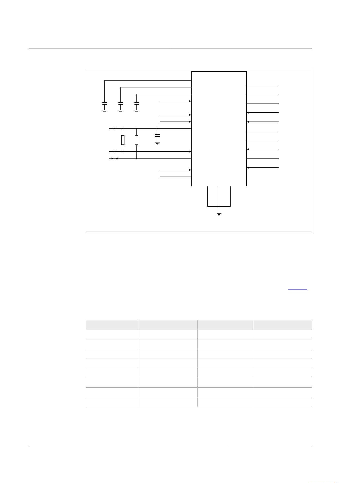
NXP Semiconductors
PF81
aaa- 0406 22
29
42
20
22
23
21
24
19
49
48
57
45
51
GND
FSOB
PGOOD
EWARN
PWRON
STANDBY
RESETB MCU
INTB
WDI
SYNCOUT
SYNCIN
AGND
DGND
EPAD
GND
V1P5A
V1P5D
VIN
TBBEN
VDDOTP
VDDIO
LICELL
41
40
50
46
14
53
55
56
39
52
54
C11
1 µF
C10
0.1 µFR2
2.2 kΩ
R1
2.2 kΩ
C15
1 µF
C14
1 µF
GND
GND
GND
SCL
SDA
XINTB
AMUX
VDDIO
SCL
SDA
AN13107
PF series PMIC I2C-bus communication overview
Figure 1. I2C-bus pull-up connection
2.2 General I2C-bus operation
The PF series PMICs operate as slave devices, therefore, they will not transmit data
unless they have been addressed by the master. To allow a multi-PMIC architecture
under the same I2C-bus, the PF devices provide a selectable I2C-bus slave address set
via the one time programmable (OTP) configuration.
The OTP_I2C_ADD[2:0] is used to select the 7-bit I2C-bus address as shown in Table 1.
The 8-bit address is calculated based on the read/write operation as follows:
8-bit slave address = (7-bit address ≪ 1) + R/W
Table 1. Voltage regulator summary
OTP_I2C_ADD[2:0] 7-bit I2C-bus address 8-bit write address 8-bit read address
During try before buy (TBB) operation, the 7-bit I2C-bus address is set to 08h. Therefore,
on multi-PMIC systems it is recommended to select a different address for both devices
to allow easier debug access during development phase.
AN13107 All information provided in this document is subject to legal disclaimers. © NXP B.V. 2021. All rights reserved.
Application note Rev. 1 — 23 February 2021
000 08h 10h 11h
001 09h 12h 13h
010 0Ah 14h 15h
011 0Bh 16h 17h
100 0Ch 18h 19h
101 0Dh 1Ah 1Bh
110 0Eh 1Ch 1Dh
111 0Fh 1Eh 1Fh
4 / 20
Page 5
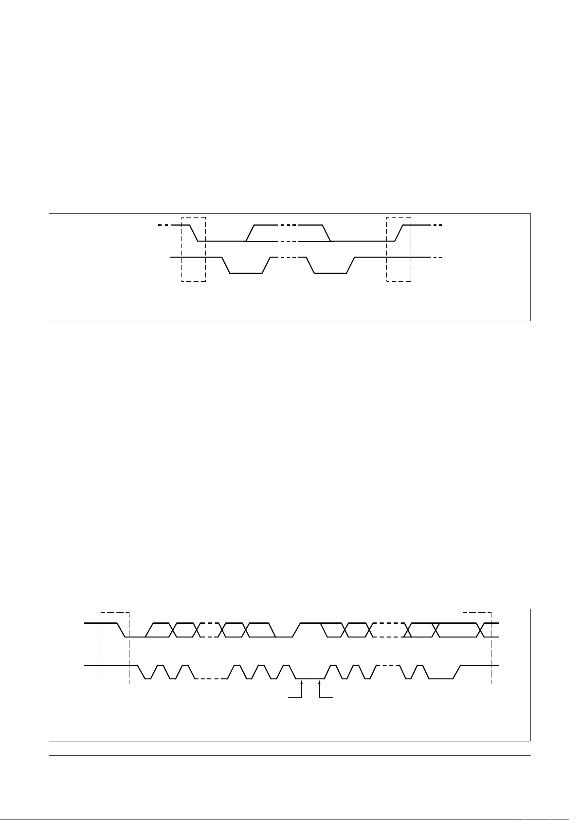
NXP Semiconductors
mba608
SDA
SCL
P
STOP condition
S
START condition
S or Sr Sr or P
SDA
SCL
MSB
1 2 7 8 9 1 2 3 to 8 9
ACK ACK
002aac861
START or
repeated START
condition
STOP or
repeated START
condition
acknowledgement
signal from slave
byte complete,
interrupt within slave
clock line held LOW
while interrupts are serviced
P
Sr
acknowledgement
signal from receiver
2.2.1 START and STOP conditions
All transactions begin with a START (S) condition and end with a STOP (P) condition.
• A HIGH to LOW transition on the SDA line while SCL is HIGH defines a START
condition.
• A LOW to HIGH transition on the SDA line while SCL is HIGH defines a STOP
condition.
Figure 2. START and STOP conditions
The master always generates the START and STOP conditions. The bus is considered to
be busy after the START condition. The bus is considered to be free again a certain time
after the STOP condition.
AN13107
PF series PMIC I2C-bus communication overview
2.2.2 Repeated START condition
A repeated START (Sr) condition is similar to a START condition and is used in place
of a back-to-back STOP then START condition. It looks identical to a START condition,
but differs from a START condition because it happens before a STOP condition (when
the bus is not idle). This operation is useful when the master wishes to start a new
communication, but does not wish to let the bus go idle with the STOP condition,
preventing the master from losing control of the bus to another master (in multi-master
environments).
2.2.3 Byte format
Every byte put on the SDA line must be eight bits long. The number of bytes that can be
transmitted per transfer is unrestricted. An acknowledge bit must follow each byte. Data
is transferred with the most significant bit (MSB) first. If a slave cannot receive or transmit
another complete byte of data until it has performed some other function, for example
servicing an internal interrupt, it can hold the clock line SCL LOW to force the master into
a wait state. Data transfer then continues when the slave is ready for another byte of data
and releases clock line SCL.
Figure 3. Data transfer on the I2C-bus
AN13107 All information provided in this document is subject to legal disclaimers. © NXP B.V. 2021. All rights reserved.
Application note Rev. 1 — 23 February 2021
5 / 20
Page 6

NXP Semiconductors
mba607
data line
stable;
data valid
change
of data
allowed
SDA
SCL
2.2.4 Acknowledge (ACK) and not acknowledge (NACK)
The acknowledge takes place after every byte. The acknowledge bit allows the receiver
to signal the transmitter that the byte was successfully received and another byte may be
sent. The master generates all clock pulses, including the acknowledge ninth clock pulse.
The acknowledge signal is defined as follows: the transmitter releases the SDA line
during the acknowledge clock pulse so the receiver can pull the SDA line LOW and
it remains stable LOW during the HIGH period of this clock pulse. Set-up and hold
times must also be taken into account. Refer to document UM10204 for detailed timing
description.
When SDA remains HIGH during this ninth clock pulse, it is defined as the not
acknowledge signal. The master can then generate either a STOP condition to abort the
transfer, or a repeated START condition to start a new transfer. There are five conditions
that lead to the generation of a NACK:
1. No receiver is present on the bus with the transmitted address so there is no device to
2. The receiver is unable to receive or transmit because it is performing some real-time
3. During the transfer, the receiver gets data or commands that it does not understand.
4. During the transfer, the receiver cannot receive any more data bytes.
5. A master-receiver must signal the end of the transfer to the slave transmitter.
AN13107
PF series PMIC I2C-bus communication overview
respond with an acknowledge.
function and is not ready to start communication with the master.
2.2.5 Data validity
The data on the SDA line must be stable during the HIGH period of the clock. The HIGH
or LOW state of the data line can only change when the clock signal on the SCL line is
LOW. One clock pulse is generated for each data bit transferred.
Figure 4. Bit transfer on the I2C-bus
AN13107 All information provided in this document is subject to legal disclaimers. © NXP B.V. 2021. All rights reserved.
Application note Rev. 1 — 23 February 2021
6 / 20
Page 7

NXP Semiconductors
2.3 Bus speeds
The PF series PMICs are compatible with the following I2C-bus standard speeds:
• Standard mode (100 kbit/s)
• Fast mode (400 kbit/s)
• Fast-mode Plus (1 Mbit/s)
• High-speed mode (3.4 Mbit/s)
2.3.1 Fast mode (400 kbit/s)
Fast mode devices can receive and transmit at up to 400 kbit/s. The minimum
requirement is that they can synchronize with a 400 kbit/s transfer. They can then prolong
the LOW period of the SCL signal to slow down the transfer. The protocol, format, logic
levels and maximum capacitive load for the SDA and SCL lines are the same as the
Standard mode I2C-bus specification.
Fast mode devices are downward compatible and can communicate with Standard mode
devices in a 0 kbit/s to 100 kbit/s I2C-bus system.
AN13107
PF series PMIC I2C-bus communication overview
2.3.2 Fast-mode Plus (1 Mbit/s)
Fast-mode Plus (Fm+) devices offer an increase in I2C-bus transfer speeds and total
bus capacitance. Fm+ devices can transfer information at bit rates of up to 1 Mbit/s. Yet
they remain fully downward compatible with Fast mode or Standard mode devices for
bidirectional communication in a mixed-speed bus system. The same serial bus protocol
and data format are maintained as with the Fast mode or Standard mode system.
2.3.3 High-speed mode (3.4 Mbit/s)
High-speed mode (Hs mode) devices offer a quantum leap in I2C-bus transfer speeds.
Hs mode devices can transfer information at bit rates of up to 3.4 Mbit/s. Yet they
remain fully downward compatible with Fast-mode Plus, Fast mode or Standard mode
(F/S mode) devices for bidirectional communication in a mixed-speed bus system. With
the exception that arbitration and clock synchronization is not performed during the
Hs mode transfer, the same serial bus protocol and data format are maintained as with
the F/S mode system.
The PF series PMICs does not provide dedicated SDAH and SCLH signal, however the
SDA and SCL lines are used to operate at either speed.
2.3.3.1 Entering High-speed mode
By default, the PMIC devices operate in F/S mode (Fast mode, compatible with Standard
mode). They can switch from Fast mode to Hs mode and back controlled by the serial
transfer on the I2C-bus.
Before time t1 in Figure 5, each connected device operates in F/S mode. Between
times t1 and tH (this time interval can be stretched by any device) the master sends
a high-speed request sequence ‘S 00001XXX A’ which must be recognized by every
device in the bus. Between times t1 and tH, the connected master and slave devices
switch its internal circuit from the F/S mode to the High-speed mode setting.
AN13107 All information provided in this document is subject to legal disclaimers. © NXP B.V. 2021. All rights reserved.
Application note Rev. 1 — 23 February 2021
7 / 20
Page 8

NXP Semiconductors
msc618
8-bit master code 0000 1xxx
A
t
H
t
1
S
F/S mode
HS mode
If P then
F/S mode
If Sr (dotted lines)
then HS mode
1 6 7 8 9 6 7 8 91
1 2 to 5
2 to 5
2 to 5
6 7 8 9
SDA high
SCL high
SDA high
SCL high
t
H
t
FS
Sr Sr P
n + (8-bit data + A/A)
7-bit SLA
R/W A
= Master current source pull-up
= Resistor pull-up
AN13107
PF series PMIC I2C-bus communication overview
Figure 5. A complete Hs mode transfer
2.3.3.2 Exiting High-speed mode
At time tFS in Figure 5, each connected device must recognize the STOP condition (P)
and switch its internal circuit from the Hs mode setting back to the Fast mode setting as
present before time t1. This operation must be completed within the minimum bus free
time as specified in the Fast mode specification.
2.4 I2C-bus write operation
To write data to a device through the I2C-bus, the following steps must be followed:
1. The master must send a START condition on the bus along with the 7 bits of the slave
address plus the R/W bit = 0 to announce that the transaction is a write command.
2. After the slave sends the acknowledge bit, the master will then send the register
address of the register it wishes to write to. The slave acknowledges again, letting the
master know it is ready to receive the data.
3. The master starts sending the register data to the slave, until the master has sent
all the data it needs (one or more bytes). At the end of every data byte, the slave
provides an ACK bit to let the master know it is ready to get the next byte.
4. The master terminates the transmission with a STOP condition.
AN13107 All information provided in this document is subject to legal disclaimers. © NXP B.V. 2021. All rights reserved.
Application note Rev. 1 — 23 February 2021
8 / 20
Page 9

NXP Semiconductors
aaa-0 40623
X00000 10
1S2 3 4 5 6 7 8 9 1 2 3 4 5 6 7 8 9 1 2 3 4 5 6 7 8 9
0
SDA
SCL
X X X X X X X X X X X X X X X
ACK8-bit w rite dataACKACKR/W 8-bit regist er address7-bit slave ad dress
P
aaa- 0406 24
8-bit register ad dress7-bit slave address
8-b it CRC8-bit write data ACK
ACKR/W
ACK
ACK
1 2 3 4 5 6 7 8 9 1 2 3 4 6 7 8 9
P
X X X XX X X XX X X XX X X X
5 6 7 81 2 3 4 5 6 7 8 99 1 2 3 4
X X X XX000000
S
0
SCL
SDA
SCL
SDA 1 X X X
5
Figure 6. I2C-bus write command
2.4.1 I2C-bus write with CRC verification
When the I2C-bus cyclic redundancy check (CRC) function is enabled on the PMIC, the
write command must add the calculated CRC byte after the data byte being written.
AN13107
PF series PMIC I2C-bus communication overview
Figure 7. I2C-bus write command with CRC
For detail description on how to calculate the CRC, see Section 3.
2.5 I2C-bus read operation
In order to read from a slave:
1. The master must first instruct the slave, which register it wishes to read from. The
master starting off the transmission by sending the slave address with the R/W bit
equal to logic 0 (signifying a write), followed by the register address it wishes to read
from.
AN13107 All information provided in this document is subject to legal disclaimers. © NXP B.V. 2021. All rights reserved.
Application note Rev. 1 — 23 February 2021
2. Once the slave acknowledges this register address, the master will send a START
condition again, followed by the slave address with the R/W bit set to logic 1
(signifying a read). This time, the slave acknowledges the read request, and the
master releases the SDA bus, but continues supplying the clock to the slave. During
this part of the transaction, the master becomes the master-receiver, and the slave
becomes the slave-transmitter.
3. The master continues sending out the clock pulses, but releases the SDA line, so that
the slave can transmit data. At the end of every data byte, the master sends an ACK
to the slave, letting the slave know that it is ready for more data.
9 / 20
Page 10

NXP Semiconductors
aaa- 0406 25
8-bit register ad dress7-bit slave address
8-b it data from slave7-bit slave address ACK
ACKR/W
R/W NACK
ACK
1 2 3 4 5 6 7 8 9 1 2 3 4 6 7 8 9
P
X X X XX X X X0 0 0 10 0 0 1
5 6 7 81 2 3 4 5 6 7 8 99 1 2 3 4
X X X XX000000
S
Sr
0
SCL
SDA
SCL
SDA 1 X X X
5
aaa-0 40626
X10000 10
1Sr2 3 4 5 6 7 8 9 1 2 3 4 5 6 7 8 9 1 2 3 4 5 6 7 8 9
0
SDA
SCL
X X X X X X X X X X X X X X X
NACK8-bit CRC from slaveACKACKR/W 8-bit d ata from slave7-bit slave ad dress
X00000 10
1S2 3 4 5 6 7 8 9 1 2 3 4 5 6 7 8 9
0
SDA
SCL
X X X X X X X
ACKACKR/W 8 -bit register ad dress7-bit slave addre ss
P
4. Once the master has received the number of bytes it is expecting, it sends a NACK,
5. The master then finishes the communication with a STOP condition.
AN13107
PF series PMIC I2C-bus communication overview
signaling to the slave to halt communications and release the bus.
Figure 8. I2C-bus read command
2.5.1 I2C-bus read with CRC verification
When the CRC function is enabled on the PMIC, there is no need for the master to
calculate or provide a CRC byte to the slave.
Reading a slave device with a simple read command as shown in Figure 8, still extracts
the correct data from the corresponding registers. However, since the CRC function is
enabled, the PMIC expects one more byte to be extracted so that it can provide the CRC
calculated internally.
Therefore, the master must make sure to request two bytes from the slave on the read
transaction.
Figure 9. I2C-bus read command with CRC
Although not mandatory, it is the responsibility of the master device to use the CRC
provided by the slave to confirm that the data provided is valid by calculating the CRC
AN13107 All information provided in this document is subject to legal disclaimers. © NXP B.V. 2021. All rights reserved.
Application note Rev. 1 — 23 February 2021
10 / 20
Page 11

NXP Semiconductors
aaa-04 0627
X00000 10
1S2 3 4 5 6 7 8 9 1 2 3 4 5 6 7 8 9 1 2 3 4 5 6 7 8 9
0
SDA
SCL
X X X X X X X X X X X X X X X
ACK8-bit write da taACKACKR/W 8-b it register START addr ess
X X X X X X X X
ACK8-bit write da ta
7-bit slave ad dress
P
1 2 3 4 5 6 7 8 9
X X X X X X X X
ACK8-bit write da ta
1 2 3 4 5 6 7 8 9
X X X X X X X X
ACK8-bit write da ta
1 2 3 4 5 6 7 8 9
internally using the slave address + register address + data byte and comparing it with
the CRC provided by the slave.
2.6 I2C-bus Burst mode
The PF series PMICs feature a Burst mode intended for fast reading or writing of
consecutive registers in the register map. A burst write uses the initial register address as
the base address. The device increases the register address by one every data byte is
clocked in or out of the corresponding indexed address.
The Burst mode is applicable to I2C-bus transactions with or without CRC enabled using
the following structure.
2.6.1 Burst write
To write several registers in Burst mode, the master must send the first data byte
including the slave address+ R/W + register address + data byte. Instead of sending
a STOP or START bit, the master device must keep sending as many data bytes as it
wants to push into the list of consecutive I2C-bus addresses. At the end of the last data
byte, the master must send a STOP bit to finish the burst write transaction.
AN13107
PF series PMIC I2C-bus communication overview
Figure 10. Standard burst write
Likewise, to write in Burst mode with the CRC enabled, the master must send
consecutive pairs of data + CRC bytes. The digital controller increases the register
address once it receives two bytes.
AN13107 All information provided in this document is subject to legal disclaimers. © NXP B.V. 2021. All rights reserved.
Application note Rev. 1 — 23 February 2021
11 / 20
Page 12

NXP Semiconductors
aaa-0 40628
X00000 10
1S2 3 4 5 6 7 8 9 1 2 3 4 5 6 7 8 9
0SDA
SCL
SDA
SCL
SDA
SCL
SDA
SCL
X X X X X X X
ACKACKR/W 8-bit register START address
X X X X X X X X
ACK8-bit w rite data
7-bit slave address
P
1 2 3 4 5 6 7 8 9
X X X X X X X X
ACK8-bit CRC
1 2 3 4 5 6 7 8 9
X X X X X X X X
ACK8-bit w rite data
1 2 3 4 5 6 7 8 9
X X X X X X X X
ACK8-bit CRC
1 2 3 4 5 6 7 8 9
X X X X X X X X
ACK8-bit w rite data
1 2 3 4 5 6 7 8 9
X X X X X X X X
ACK8-bit CRC
1 2 3 4 5 6 7 8 9
Calculating the CRC in Burst mode is the same as a standard write transaction, making
sure that each CRC calculation uses the corresponding register address to which the
data is written.
For example, to burst write three bytes with CRC the following should be considered:
DEV_ADDR = 08h + R/W = 10h
START_ADDR = 00h
DATA1 = 04h
DATA2 = F4h
DATA3 = A5h
The CRCs are calculated:
CRC1 = CRC_CALC (DEV_ADDR, START_ADD, DATA1)
CRC2 = CRC_CALC (DEV_ADDR, START_ADD + 1, DATA2)
CRC3 = CRC_CALC (DEV_ADDR, START_ADD + 2, DATA3)
Where CRC_CALC is the function to calculate the CRC value using the parameters
inside the parenthesis.
AN13107
PF series PMIC I2C-bus communication overview
Figure 11. Burst write with CRC
AN13107 All information provided in this document is subject to legal disclaimers. © NXP B.V. 2021. All rights reserved.
Application note Rev. 1 — 23 February 2021
12 / 20
Page 13

NXP Semiconductors
2.6.2 Burst read
To read several registers in Burst mode, the master must first send the initial write
command to determine the starting register to read from, followed by the slave address
plus the R/W = 1. Then, the master must clock as many bytes out of the PMIC as
desired.
The master returns an ACK after each byte read. It returns a NACK when it is done
getting data from the PMIC, followed by a STOP bit.
AN13107
PF series PMIC I2C-bus communication overview
AN13107 All information provided in this document is subject to legal disclaimers. © NXP B.V. 2021. All rights reserved.
Application note Rev. 1 — 23 February 2021
13 / 20
Page 14

NXP Semiconductors
aaa- 0406 29
8-bit register START ad dress7-bit slave address
8-b it data from slave7-bit slave address ACK
ACKR/W
R/W
ACK
ACK
1 2 3 4 5 6 7 8 9 1 2 3 4 6 7 8 9
X X X XX X X X0 0 0 10 0 0 1
5 6 7 81 2 3 4 5 6 7 8 99 1 2 3 4
X X X XX000000
S
Sr
P
0
SCL
SDA
SCL
SDA 1 X X X
5
8-b it data from slave ACK
1 2 3 4 6 7 8 9
X X X XX X X X
5
8-b it data from slave ACK
1 2 3 4 6 7 8 9
X X X XX X X X
5
8-b it data from slave NACK
1 2 3 4 6 7 8 9
X X X XX X X X
5
AN13107
PF series PMIC I2C-bus communication overview
Figure 12. Standard burst read
To read several registers in Burst mode with the CRC enabled, the master must first send
the initial write command to determine the starting register to read from, followed by the
slave address plus the R/W = 1. Then, the master must clock two bytes (data + CRC) per
each register read.
The master returns an ACK after each byte read. It returns a NACK when the last CRC
byte is received from the PMIC, followed by a STOP bit.
AN13107 All information provided in this document is subject to legal disclaimers. © NXP B.V. 2021. All rights reserved.
Application note Rev. 1 — 23 February 2021
14 / 20
Page 15

NXP Semiconductors
X00000 10
1S2 3 4 5 6 7 8 9 1 2 3 4 5 6 7 8 9
0
SDA
SCL
SDA
SCL
SDA
SCL
X X X X X X X
ACKACKR/W 8-bit regis ter START address
X X X X X X X X
ACK8-bi t data from slave
7-bit slave ad dress
10000 10
1Sr2 3 4 5 6 7 8 9
0
SDA
SCL
ACKR/W7-bit slave ad dress
1 2 3 4 5 6 7 8 9
X X X X X X X X
ACK8-bit CRC fr om slave
1 2 3 4 5 6 7 8 9
X X X X X X X X
ACK8-bi t data from slave
1 2 3 4 5 6 7 8 9
X X X X X X X X
ACK8-bit CRC
1 2 3 4 5 6 7 8 9
X X X X X X X X
ACK8-bi t data from slave
1 2 3 4 5 6 7 8 9
X X X X X X X X
ACK8-bit CRC
1 2 3 4 5 6 7 8 9
aaa-04 0630
SDA
SCL
P
X X X X X X X X
ACK8-bi t data from slave
1 2 3 4 5 6 7 8 9
X X X X X X X X
NACK8-bit CRC
1 2 3 4 5 6 7 8 9
AN13107
PF series PMIC I2C-bus communication overview
Figure 13. Burst read with CRC
During a burst read, the master is not required to calculate the CRC bytes to execute
the read transaction. However, if the master device implements a CRC verification after
getting each data byte from the PMIC, the CRC must be calculated for each data byte,
considering the slave address as 7-bit address + 1 (read). The register address should
be calculated as the START address + n, where n is the index of the burst data received
from the PMIC.
3 I2C-bus CRC calculation
3.1 CRC verification strategy
The PF series PMICs feature a selectable CRC function to ensure the integrity of the
data transmitted to and from the PMIC. This mechanism is key in providing latent fault
coverage for safety system by protecting the system from misconfiguration due to
possible interference on the I2C-bus.
AN13107 All information provided in this document is subject to legal disclaimers. © NXP B.V. 2021. All rights reserved.
Application note Rev. 1 — 23 February 2021
15 / 20
Page 16

NXP Semiconductors
aaa- 0406 31
MSB
data
7 6 5 4 3 2 1 0
The I2C-bus CRC is enabled by default via the OTP_I2C_CRC_EN bit in the OTP
configuration.
The recommended CRC verification strategy should be as follows:
1. During a write operation, the MCU must calculate the CRC using the slave address,
2. The I2C-bus command must include the CRC byte at the end of the package.
3. If the data suffered an alteration during the transmission, the PMIC finds the
4. During a read operation, the MCU must request two data bytes from the PMIC (data +
5. The MCU should use the data provided by the PMIC to calculate CRC internally and
6. If the data received by the MCU does not match the CRC provided by the PMIC, the
AN13107
PF series PMIC I2C-bus communication overview
register address, and data sent.
discrepancy when it calculates the CRC with the actual data received at the input
buffer. It ignores the write command and it sets the CRC_I flag to notify an error has
occurred.
a. It is up to the system designer to enable the CRC_I flag to assert the INTB pin or
not by clearing or setting the CRC_M mask.
b. If the CRC_I interrupt is masked, the system can still acknowledge and service a
bad CRC interrupt by polling the interrupt registers.
CRC).
compare against the CRC provided by the PMIC.
MCU should disregard the information and request the data again before performing
any action with it.
3.2 I2C-bus CRC implementation
The PF series PMICs implement a standard CRC8 Society of Automotive Engineers
(SAE) as defined in the SAE J1850 specification with the following characteristics:
• Polynomial = 1Dh
• Initial value (seed) = FFh
• Generator polynom: x8 + x4 + x3 + x2 + 1
Figure 14. I2C-bus CRC polynomial
The CRC is calculated by shifting 24-bit data through the polynomial. The 24-bit package
is built as follows:
DEVICE_ADDR[b8] + REGISTER_ADDR[b8] + DATA[b8]
Where the DEVICE_ADDR is the 7-bit slave address plus the corresponding read/write
bit.
AN13107 All information provided in this document is subject to legal disclaimers. © NXP B.V. 2021. All rights reserved.
Application note Rev. 1 — 23 February 2021
16 / 20
Page 17

NXP Semiconductors
For example to write a PMIC with 7-bit address set to 08h, writing the register address
9Fh with data 01h, byte 1 through byte 3 are used as follows:
• Byte 1: (08h ≪ 1) + 0 = 10h
• Byte 2: 9Fh
• Byte 3: 01h
• CRC = D5h
Figure 15. I2C-bus write with CRC byte example
3.2.1 CRC calculation example
There are several ways to calculate the CRC. This document presents a simple C code
to calculate the CRC by shifting the 24-bit data into the CRC using for loops.
AN13107
PF series PMIC I2C-bus communication overview
unsigned char CRC_CALC (char devAD, char reg, char data)
{
unsigned char inbit = 0x00;
unsigned char outbit = 0x00;
unsigned char P = 0x1D;
unsigned char res = 0xFF; /* initialize CRC register with FF */
/* Shift out the MSB of each input byte and put it into the next Byte */
for (int i = 0 ; i < 24; i++)
{
/* Xor the msb from Message and the msb from CRC calculation */
inbit = (devAD & 0x80)>> 7;
outbit = (res & 0x80) >> 7;
if ((inbit ^ outbit) == 1)
{ /* If XOR is 1 then shift the CRC and Apply XOR */
res = res << 1;
res = res ^ P; }
else
{ /* if XOR is 0 then shift the CRC register only */
res = res << 1; }
devAD = devAD << 1;
if((reg & 0x80) == 0x80)
{ devAD = devAD + 1; }
reg = reg << 1;
if((data & 0x80) == 0x80)
{ reg = reg + 1; }
data = data << 1;
}
return (res);
}
AN13107 All information provided in this document is subject to legal disclaimers. © NXP B.V. 2021. All rights reserved.
Application note Rev. 1 — 23 February 2021
17 / 20
Page 18

NXP Semiconductors
4 I2C-bus secure write operation
4.1 Secure write overview
The PF series PMICs feature a secure write mechanism to ensure all safety critical bits
cannot be written by mistake.
Secured registers apply the written value only if the correct secure write protocol is
followed in the right order and within a specific time. Failing to follow the secure write
protocol results in the write command being ignored and the PMIC takes no action.
The secure write sequence is as follows:
• The MCU sends the command to modify the secure register (no action taken by the
PMIC yet).
• The MCU must read the random code from the RANDOM_GEN register and write it
back into the RANDOM_CHK register in the PMIC.
As soon as the PMIC receives data in the RANDOM_CHECK registers, it compares the
RANDOM_CHK against the RANDOM_GEN register:
• If RANDOM_CHK[7:0] = RANDOM_GEN[7:0], the device applies the configuration
on the corresponding secure register, and self-clears both the RANDOM_GEN and
RANDOM_CHK registers.
• If RANDOM_CHK[7:0] is different from RANDOM_GEN[7:0], the device ignores the
configuration command and self-clears both the RANDOM_GEN and RANDOM_CHK
registers.
AN13107
PF series PMIC I2C-bus communication overview
In the event the MCU sends any other command instead of providing a value for the
RANDOM_CHK register, the PMIC cancels the ongoing secure write transaction and
performs the new I2C-bus command.
In the event the MCU does not provide a value for the RANDOM_CHK register, the
I2C-bus transaction will time out 10 ms after the RANDOM_GEN code is generated, and
the device is ready for a new transaction.
4.2 Secure registers
In the PF series PMICs, the secure write protocol is applicable only to bits listed as
secure bits. By definition, the secure bits are typically functional bits which are intended
to enable or disable a safety mechanism, or read safety notification that is important for
the system functional safety strategy. However, the list of secure bits may differ from one
device to another.
To find the detailed list of secure bits for each device, refer to the corresponding product
data sheet.
AN13107 All information provided in this document is subject to legal disclaimers. © NXP B.V. 2021. All rights reserved.
Application note Rev. 1 — 23 February 2021
18 / 20
Page 19

NXP Semiconductors
5 Legal information
5.1 Definitions
Draft — A draft status on a document indicates that the content is still
under internal review and subject to formal approval, which may result
in modifications or additions. NXP Semiconductors does not give any
representations or warranties as to the accuracy or completeness of
information included in a draft version of a document and shall have no
liability for the consequences of use of such information.
5.2 Disclaimers
Limited warranty and liability — Information in this document is believed
to be accurate and reliable. However, NXP Semiconductors does not
give any representations or warranties, expressed or implied, as to the
accuracy or completeness of such information and shall have no liability
for the consequences of use of such information. NXP Semiconductors
takes no responsibility for the content in this document if provided by an
information source outside of NXP Semiconductors. In no event shall NXP
Semiconductors be liable for any indirect, incidental, punitive, special or
consequential damages (including - without limitation - lost profits, lost
savings, business interruption, costs related to the removal or replacement
of any products or rework charges) whether or not such damages are based
on tort (including negligence), warranty, breach of contract or any other
legal theory. Notwithstanding any damages that customer might incur for
any reason whatsoever, NXP Semiconductors’ aggregate and cumulative
liability towards customer for the products described herein shall be limited
in accordance with the Terms and conditions of commercial sale of NXP
Semiconductors.
Right to make changes — NXP Semiconductors reserves the right to
make changes to information published in this document, including without
limitation specifications and product descriptions, at any time and without
notice. This document supersedes and replaces all information supplied prior
to the publication hereof.
Applications — Applications that are described herein for any of these
products are for illustrative purposes only. NXP Semiconductors makes
no representation or warranty that such applications will be suitable
for the specified use without further testing or modification. Customers
are responsible for the design and operation of their applications and
products using NXP Semiconductors products, and NXP Semiconductors
accepts no liability for any assistance with applications or customer product
design. It is customer’s sole responsibility to determine whether the NXP
Semiconductors product is suitable and fit for the customer’s applications
and products planned, as well as for the planned application and use of
customer’s third party customer(s). Customers should provide appropriate
design and operating safeguards to minimize the risks associated with
their applications and products. NXP Semiconductors does not accept any
liability related to any default, damage, costs or problem which is based
AN13107
PF series PMIC I2C-bus communication overview
on any weakness or default in the customer’s applications or products, or
the application or use by customer’s third party customer(s). Customer is
responsible for doing all necessary testing for the customer’s applications
and products using NXP Semiconductors products in order to avoid a
default of the applications and the products or of the application or use by
customer’s third party customer(s). NXP does not accept any liability in this
respect.
Suitability for use in automotive applications — This NXP
Semiconductors product has been qualified for use in automotive
applications. Unless otherwise agreed in writing, the product is not designed,
authorized or warranted to be suitable for use in life support, life-critical or
safety-critical systems or equipment, nor in applications where failure or
malfunction of an NXP Semiconductors product can reasonably be expected
to result in personal injury, death or severe property or environmental
damage. NXP Semiconductors and its suppliers accept no liability for
inclusion and/or use of NXP Semiconductors products in such equipment or
applications and therefore such inclusion and/or use is at the customer's own
risk.
Export control — This document as well as the item(s) described herein
may be subject to export control regulations. Export might require a prior
authorization from competent authorities.
Translations — A non-English (translated) version of a document is for
reference only. The English version shall prevail in case of any discrepancy
between the translated and English versions.
Security — Customer understands that all NXP products may be subject
to unidentified or documented vulnerabilities. Customer is responsible
for the design and operation of its applications and products throughout
their lifecycles to reduce the effect of these vulnerabilities on customer’s
applications and products. Customer’s responsibility also extends to other
open and/or proprietary technologies supported by NXP products for use
in customer’s applications. NXP accepts no liability for any vulnerability.
Customer should regularly check security updates from NXP and follow up
appropriately. Customer shall select products with security features that best
meet rules, regulations, and standards of the intended application and make
the ultimate design decisions regarding its products and is solely responsible
for compliance with all legal, regulatory, and security related requirements
concerning its products, regardless of any information or support that may
be provided by NXP. NXP has a Product Security Incident Response Team
(PSIRT) (reachable at PSIRT@nxp.com) that manages the investigation,
reporting, and solution release to security vulnerabilities of NXP products.
5.3 Trademarks
Notice: All referenced brands, product names, service names and
trademarks are the property of their respective owners.
NXP — wordmark and logo are trademarks of NXP B.V.
AN13107 All information provided in this document is subject to legal disclaimers. © NXP B.V. 2021. All rights reserved.
Application note Rev. 1 — 23 February 2021
19 / 20
Page 20

NXP Semiconductors
Contents
1 Introduction ......................................................... 3
2 I2C-bus overview .................................................3
2.1 I2C-bus hardware considerations ...................... 3
2.2 General I2C-bus operation ................................ 4
2.2.1 START and STOP conditions ............................ 5
2.2.2 Repeated START condition ............................... 5
2.2.3 Byte format ........................................................ 5
2.2.4 Acknowledge (ACK) and not acknowledge
(NACK) ...............................................................6
2.2.5 Data validity ....................................................... 6
2.3 Bus speeds ........................................................7
2.3.1 Fast mode (400 kbit/s) ...................................... 7
2.3.2 Fast-mode Plus (1 Mbit/s) ................................. 7
2.3.3 High-speed mode (3.4 Mbit/s) ........................... 7
2.3.3.1 Entering High-speed mode ................................7
2.3.3.2 Exiting High-speed mode .................................. 8
2.4 I2C-bus write operation ..................................... 8
2.4.1 I2C-bus write with CRC verification ................... 9
2.5 I2C-bus read operation ......................................9
2.5.1 I2C-bus read with CRC verification ..................10
2.6 I2C-bus Burst mode ........................................ 11
2.6.1 Burst write ........................................................11
2.6.2 Burst read ........................................................ 13
3 I2C-bus CRC calculation .................................. 15
3.1 CRC verification strategy ................................. 15
3.2 I2C-bus CRC implementation .......................... 16
3.2.1 CRC calculation example ................................ 17
4 I2C-bus secure write operation ........................18
4.1 Secure write overview ..................................... 18
4.2 Secure registers .............................................. 18
5 Legal information .............................................. 19
AN13107
PF series PMIC I2C-bus communication overview
Please be aware that important notices concerning this document and the product(s)
described herein, have been included in section 'Legal information'.
© NXP B.V. 2021. All rights reserved.
For more information, please visit: http://www.nxp.com
For sales office addresses, please send an email to: salesaddresses@nxp.com
Date of release: 23 February 2021
Document identifier: AN13107
 Loading...