

Page 1

AN10364
Opto-electrical isolation of the I2C-bus (operating the bus
between points with different local ground potential)
Rev. 1 — 12 November 2010 Application note
Document information
Info Content
Keywords P82B96, PCA9600, PCA9601, RS-485, I2C-bus, Fast-mode Plus, CAN
bus, opto-isolation, safety isolation, PoE
2
Abstract This report discusses factors that need consideration when an I
used to communicate between two points that do not share a common
logic ground potential. I
and it is expected that connected devices share that reference.
In practice, when an I2C-bus is extended to link devices that are separated
by distances exceeding about 1 meter there can be many factors that
cause differences in the local ground potential of those devices and that in
turn affects the noise margins of the system and can lead to device ratings
being exceeded.
In other cases where an I2C-bus could provide an attractive data link there
is no possibility for a shared ground reference. Examples include the need
to provide safety isolation between the I
power, telephone lines, or patient monitoring medical equipment. In other
cases, such as Power over Ethernet, standards require isolation of the
grounds.
Solutions are provided to deal with ground differences ranging from less
than 1 V up to kilovolt levels by using Opto or transformer isolators in the
signal path.
Key to all solutions is the availability of I2C buffers with the capability to
split the bidirectional I
logic streams that can be then be handled using conventional methods.
Solutions for links from 3 kHz to 1 MHz speeds are described.
2
C logic signals are referenced to a ground level
2
C control signals and AC mains
2
C signals into pairs of conventional uni-directional
C-bus is
Page 2

NXP Semiconductors
AN10364
Opto-electrical isolation of the I2C-bus
Revision history
Rev Date Description
v.1 20101112 application note; initial release
Contact information
For more information, please visit: http://www.nxp.com
For sales office addresses, please send an email to: salesaddresses@nxp.com
AN10364 All information provided in this document is subject to legal disclaimers. © NXP B.V. 2010. All rights reserved.
Application note Rev. 1 — 12 November 2010 2 of 16
Page 3

NXP Semiconductors
1. Introduction
The I2C-bus provides an attractive maintenance and control communication interface
between parts of a system since it uses only two signal wires yet has powerful addressing
and a reasonably fast, up to 1 MHz, bidirectional data handling capability.
2
I
C-bus logic signals are referenced to a common (ground) potential. Any potential
difference between the grounds of different devices on an I
the logic signal level between the sending and receiving devices that is equivalent to
noise-induced signal level disturbances on the bus wiring. It increases the possibility of
communication errors or exceeding the voltage ratings of the connected devices. Most
2
I
C-bus ICs have I/Os ratings that prohibit applying negative voltages greater than
0.3 V to 0.5 V. When one IC has a ground potential 1 V lower than another, then when
that IC sends a LOW of, say, +0.4 V with respect to its ground the receiving input will be
driven to 0.6 V relative to its ground and exceed its rating. Even when I
share a nominally common ground the possibility that large currents, sharing that ground,
can cause significant differences in local potential should be considered.
AN10364
Opto-electrical isolation of the I2C-bus
2
C-bus introduces a change in
2
C components
Many systems that can benefit from the advan tages of I
2
C-bus control are not allowed to
share any common reference signal (grou nd ) potential. To prevent any chance of
electrocution, AC mains control and medical patient monitoring equipment require a
safety isolation barrier, to kilovolt levels, between the system components. Regulations
require isolation from telephone lines and Standards require isolation from Ethernet
wiring, especially when power is also supplied by the Ethernet wiring (PoE). Techniques
enabling reliable I
2
C communication while addressing these different require m en ts all
require first splitting the normally bidirectional SDA/SCL signals into two uni-directional
components and then applying conventional techniques to provide the necessary
tolerance to difference in local ground potentials, or to provide total galvanic isolation.
The conventional techniques include:
• Increasing the logic signal amplitudes and limiting negative voltages using clamp
diodes.
• Conversion to differential mode signals usin g CAN or RS-485 drivers or dedicated I
2
parts
• Providing true galvanic isolation by including opto or magnetic/transformer signal
couplers
Buffers that split the I
simply re-combined by re-connecting them include P82B96, PCA9600 and PCA9601.
They can all provide the drive signals to directly interface with the isolating ICs/devices
while offering a range of I
Plus (Fm+).
2
C-bus signal into uni-directional components and allow them to be
2
C-bus interfacing speeds and drive levels including Fast-mode
C
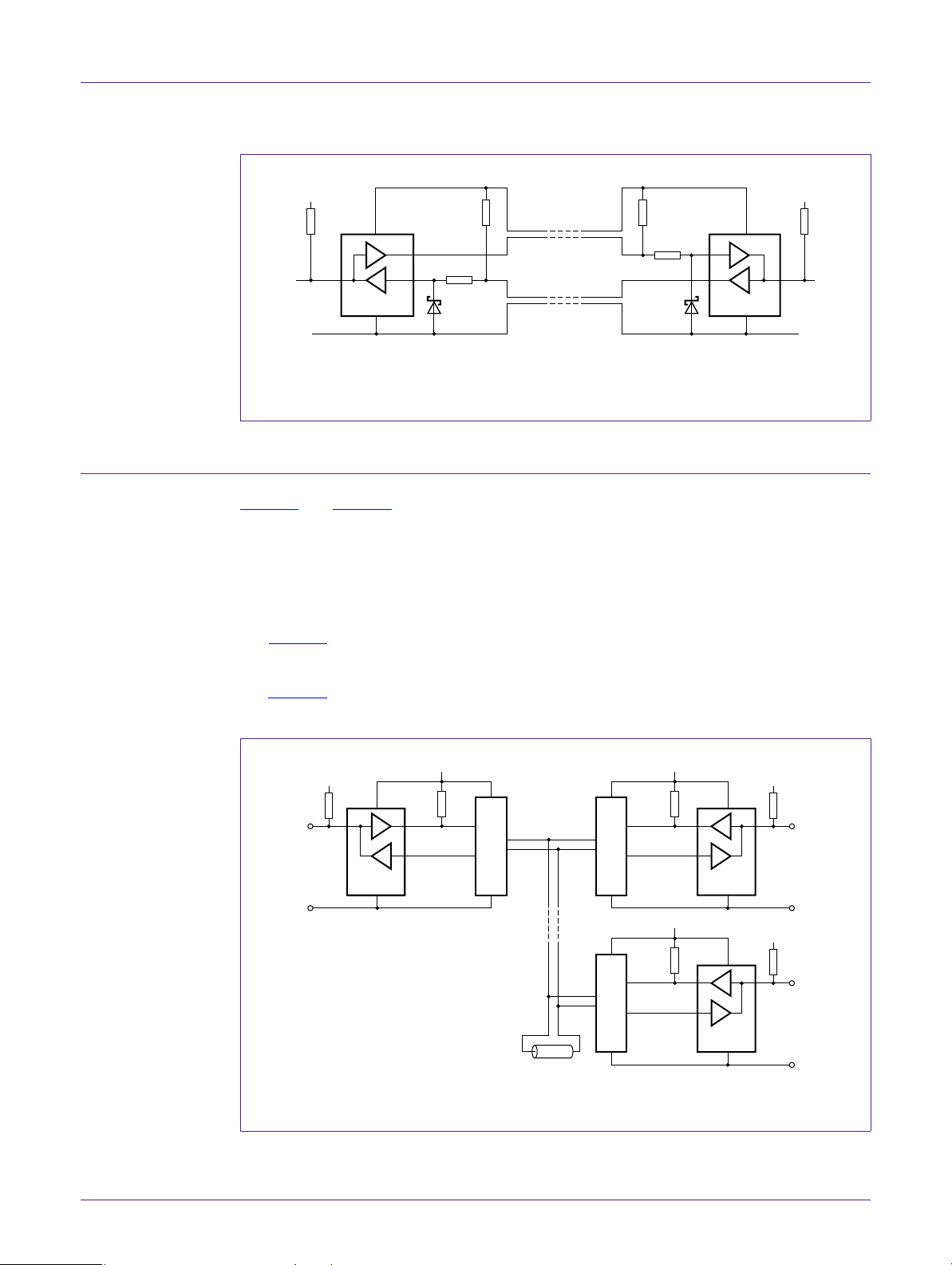
Figure 1
shows the separation of one I2C-bus signal (SDA or SCL) into two separate Send
and Receive components and clamping negative voltages with Schottky diodes as in the
‘4-signal’ arrangement discussed in AN10658 (Ref. 1
). Operating as shown with a 5 V
bus, it can operate between points having a ground potential difference of more than 2 V.
AN10364 All information provided in this document is subject to legal disclaimers. © NXP B.V. 2010. All rights reserved.
Application note Rev. 1 — 12 November 2010 3 of 16
Page 4
NXP Semiconductors
1
/
2
P82B96
SCL
002aaf769
V
CC1
2.7 kΩ
R1
150 Ω
Tx
RxSx
ground 1
V
CC
1
/2 BAT54A
1 kΩ
long wiring
5 V 5 V
R1
150 Ω
1 kΩ
1
/2 BAT54A
1
/
2
P82B96
Rx
Tx
Sx
V
CC
V
CC2
2.7 kΩ
SCL
ground 2
002aaf770
5 V
2 kΩ
1
/
2
P82B96
Tx
(SDA)
Rx
(SDA)
3.3 V
to 5 V
I2C-bus
SDA
PCA82C250
RxD
TxD
ground 3
5 V
2 kΩ
1
/
2
P82B96
Tx
(SDA)
Rx
(SDA)
3.3 V
to 5 V
I2C-bus
SDA
PCA82C250
RxD
TxD
ground 2
line termination
CANH
CANL
PCA82C250
1
/
2
P82B96
RxD
TxD
I2C-bus
SDA
Tx
(SDA)
Rx
(SDA)
2 kΩ
5 V
ground 1
3.3 V
to 5 V
AN10364
Opto-electrical isolation of the I2C-bus
Fig 1. T olerating moderate ground potential differences using separated uni-directional
signals
2. Using a differential signal technique to carry the SDA and SCL signals
Figure 2 and Figure 3 show how I2C-bus signals can be carried as differential signals over
either CAN bus hardware, that supports multi- drop bidirectional signals carried on a single
twisted pair, or RS-485 hardware that uses separate transmit and receive paths and
therefore requires using four twisted pairs to carry the two I
arrangements provide the same common-mode immunity as offered by those systems,
normally around 7V.
2
C signals. Both these
For Figure 2
duplicate this arrangement to distribute the SCL signal. Because CAN
supports the bidirectional SCL/SDA signals only two twisted pairs are required.
For Figure 3
these differential drivers are uni-direction al so fo ur twisted pairs are required
(e.g., Cat5 cable).
AN10364 All information provided in this document is subject to legal disclaimers. © NXP B.V. 2010. All rights reserved.
Application note Rev. 1 — 12 November 2010 4 of 16
Fig 2. Transmitting one I2C signal as a differential signal using CAN bus ha rdware
Page 5
NXP Semiconductors
P82B96
002aaf771
2 kΩ
Ty
Ry
Sx
ground 1
V
CC
5 V
Tx
Rx
Sy
SCL
SDA
I2C
CKT
3.3 V to 5 V
2 kΩ
1
/2 26LS31
1
/2 26LS32
long wiring
e.g., Cat5 cable
1
/2 26LS32
5 V
1
/2 26LS31
74LVC
2G07
3.3 V to 5 V
SCL
SDA
I2C
CKT
ground 2
1
/
2
P82B96
I2C-bus
SDA
002aab987
+5 V
R1
+V
CC
R2
R3
Rx
(SDA)
Tx
(SDA)
R5
R4
+V
CC1
I2C-bus
SDA
Opto-electrical isolation of the I2C-bus
Fig 3. Transmitting the I2C signals as differential signals using RS-485 hardware
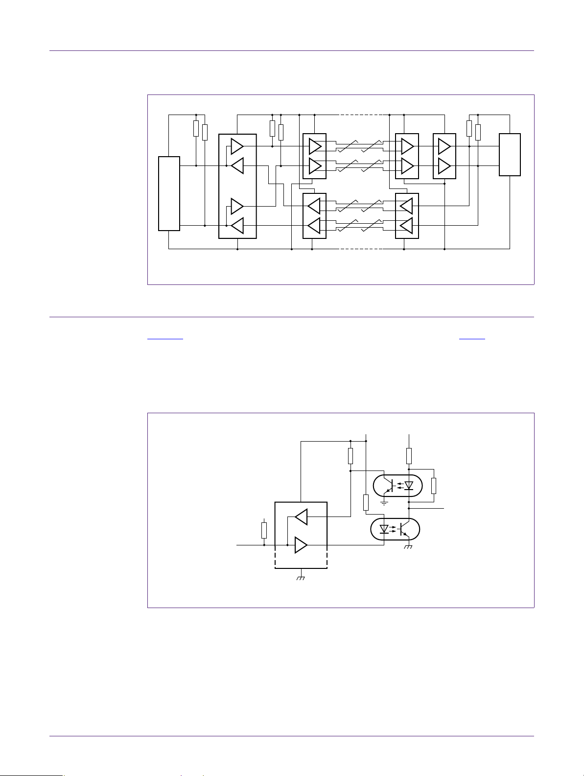
3. Opto-coupling supports very large ground differences
AN10364
Figure 4 shows the simplest arrangement from application note AN460 (Ref. 2) using
P82B96 and using the lowest cost 4N36 opto-couplers to opto-isolate the I
2
C-bus signal.
These couplers allow saturation of the photo-transistor in the opto-coupler, resulting in
very long turn-off delays caused by charge storage effects in their output transistor. For
the component values given in AN460 the total switching delays will be around 50 s and
that will limit the bus speed of this simple circuit to around 5 kHz clock.
Fig 4. Simple 5 kHz opto-electrical isolation circuit
AN10364 All information provided in this document is subject to legal disclaimers. © NXP B.V. 2010. All rights reserved.
Application note Rev. 1 — 12 November 2010 5 of 16
Page 6

NXP Semiconductors
1
/
2
P82B96
I2C-bus
SDA
002aaf778
+5 V
2.2 kΩ
Tx
(SDA)
Rx
(SDA)
usual
I
2
C-bus
pull-up
0.1 μF
560 Ω
0.1 μF
678
5
2
3
6N137 × 2
2N2907
560 Ω
+5 V
usual
I
2
C-bus
pull-up
I2C-bus
SDA
Opto-electrical isolation of the I2C-bus
4. Achieving higher opto-coupled bus speeds: 100 kHz
The clock speed allowed for any I2C class is calculated by adding the delays introduced
by the buffers and the opto-couplers to the minimum SCL ‘LOW’ period. The typical
system performance will be found to be much faster when using component s specified for
a faster class. For example using Fast-mode (Fm) parts for their smaller maximum
response delays in a Standard-m ode system. Faster speeds re quire fa ster op to-couple rs.
Parts such as 6N137 use Schottky-clamped output transistors to reduce their switching
delays to less than 100 ns (each coupler) when operating in the 5 V bus arrangement of
Figure 5
. They will ensure operation of Standard-mode systems to 100 kHz.
AN10364
Fig 5. Use higher speed opto-couple rs f or full 100 kHz oper ation
5. Opto-couplers for 400 kHz
Because the original I2C specifications did not envisage the development of bus buffering
components or the possibilities for signal propagation delays in the system, it is strictly
not allowed to introduce any delays other than those anticipated in the bus rise and fall
times unless the bus is operated at a speed lower than the maximum allowed for each
class. When buffers and opto-couplers introduce delays into the clock and data lines the
SCL LOW period should be increased by an amount equal to the sum of those delays.
Because the buffers support ‘clock stretching’ some of that increase will happen
automatically, without action by the designer. That is why a system p rogrammed for a
nominal 400 kHz will be observed to be running at a slightly slower frequency after buffers
and opto-couplers are introduced.
In practice, typical I
calculated from the bus specifications. For example, the typical response time for ICs
specified for 400 kHz application are mostly under 700 ns while the bus specifications
allow for 1.2 s delays. This means that in practice delays up to 500 ns can be tolerated.
P82B96 introduces delays around 400 ns and fast couplers will have delays less than
100 ns, so in practical systems, when the designer checks the actual bus timings,
400 kHz opto-coupling can be achieved. A fast yet simple circuit, designed for interfacing
2
C parts do not use up all of the allowed response time that can be
AN10364 All information provided in this document is subject to legal disclaimers. © NXP B.V. 2010. All rights reserved.
Application note Rev. 1 — 12 November 2010 6 of 16
Page 7

NXP Semiconductors
1
/
2
P82B96
I2C-bus
SDA
002aaf779
+3.3 V
390 Ω
Tx
(SDA)
Rx
(SDA)
use highest
possible pull-up
that gives
a reasonable
bus rise time
0.1 μF
180 Ω
0.1 μF
678
5
2
3
HCPL-060L × 2
74LVC1G07
180 Ω
+3.3 V
use lowest
pull-up,
e.g., 1 kΩ
I2C-bus
SDA
3.3 V bus components, is shown in Figure 6. The P82B96 data sheet also gives examples
of modifying the duty cycle of the clock when attempting to reach the highest speeds and
those techniques are also applicable to delays introduced by opto isolation.
AN10364
Opto-electrical isolation of the I2C-bus
In Figure 6
lowest output drive voltage (V
the reason to use the weakest pull-up on the P82B96 Sx pin is to provide the
) at Sx and therefore the highest noise margin because
OL
the indicated bus voltage is 3.3 V. Substituting PCA9600 for the P82B96 and using a
0.3 mA pull-up will provide a guaranteed V
Fig 6. Simple circuit for applications up to 400 kHz (duplicate for SCL line)
at 0.65 V and higher speed.
OL
6. Operating up to Fast-mode Plus speeds — 1 MHz
When the highest possible speed is required then all delays must be minimized and mo re
care will be required when setting the master clock timing. There is a selection of
opto-couplers with typical propagation delays in the range 40 ns to 50 ns, and some are
as low as 16 ns. When driven by PCA9600, with its typical propagation delays
40 ns to 80 ns, the total propagation delay through each coupler path can be kept below
100 ns—considerably faster than competing ‘1 MHz’ isolators using magnetic/transformer
coupling.
Figure 7
frequency. ‘Real’ means the actual observed clock frequency, not the nominal frequency
programmed into the master. Because the buffer/opto delays will cause the programmed
clock LOW period to be stretched, even the fastest system in Figure 10
clock LOW by about 130 ns and would slow a master, programmed for a nominal 1 MHz
clock, to around a ‘real’ or observed 770 kHz. Achieving a ‘real’ 1 MHz is possible but the
master must be programmed with new SCL timings that make allowance for the stretching
of the clock LOW period. After allowing for the ‘stretch’ the actual LOW period must be set
to 500 ns (minimum) to comply with the Fm+ specification.
, Figure 9 and Figure 10 show applications all capable of a real 1 MHz clock
will stretch the
AN10364 All information provided in this document is subject to legal disclaimers. © NXP B.V. 2010. All rights reserved.
Application note Rev. 1 — 12 November 2010 7 of 16
Page 8

NXP Semiconductors
PCA9600
002aaf780
Ty
Ry
Sx
V
CC
Tx
Rx
Sy
3.3 V
R1R1
I2C-bus
SCL
SDA
R1 = 1 kΩ;
all other
resistors = 390 Ω
100 nF
shield
5 V 5 V
74LVC07A
NEC / CEL
2 × PS9821-2
100 nF
SCL
SDA
I
2
C-bus
(incl. Fm+)
AN10364
Opto-electrical isolation of the I2C-bus
Fig 7. Circuit capable of Fm+ operation to 1 MHz (typical) using couplers with 50 ns (typical) delays
The example in Figure 7 uses couplers with typical delays of 50 ns and ‘conventional’
switching of the LED current using Tx, or the LVC gate, as a series switch to the ground.
When turning off, the stray capacitance of the driver and LED input must be charged
nearly to the supply before the LED current drops near zero. This increases the rise time
delay in the coupler and accounts for some additional slowing of the clock. Still, by
programming the nominal master SCL LOW to about 250 ns, to allow for 250 ns clock
‘stretching’ by PCA9600 with these 50 ns couplers, Figure 8
acknowledged address transmission at a ‘true’ 1 MHz.
In Figure 8
the top two traces show SCL/SDA at the terminals o f a master connected on
the left side while the lower traces show SCL/SDA at the terminals of an Fm+ slave
connected on the right. The dark blue trace shows SCL at the master. When the master
releases the Sx of PCA9600 the bus does not immediately rise to the V
only to the LOW level output by Sx, about 0.65 V, until the Rx pin, shown by the lower
magenta trace becomes HIGH and that HIGH at Rx propagate s bac k thr ou g h the
PCA9600 to Sx and allows it to rise to 3.3 V. The time at which SCL actually achieves the
HIGH level, starting the HIGH period of the ninth clock pulse, is indicated by the black
arrow. The ‘ste p’ at 0.65 V just prior to that time represents a holding of the master clock
LOW until the master’s input HIGH has time to propagate to the slave and back to the
master. In these traces the slave acknowledge is indicated by the red arrow on the green
slave SDA trace. Above that, and slightly delayed, is the Acknowledge LOW as received
by the master (red arrow on cyan trace). Note that LOW is valid even before the master
SCL starts to rise and, after the step of clock stretch, at least 300 ns before the master
SCL actually goes HIGH (black arrow).
shows a correctly
at 3.3 V. It rises
DD
AN10364 All information provided in this document is subject to legal disclaimers. © NXP B.V. 2010. All rights reserved.
Application note Rev. 1 — 12 November 2010 8 of 16
Page 9

NXP Semiconductors
019aaa718
AN10364
Opto-electrical isolation of the I2C-bus
PCA9621 slave at the right. Top: waveforms at left; SCL dark blue; SDA cyan.
Bottom: waveforms at right; SCL magenta; SDA green.
Remark: Nominal 5 V SMPS used was nearer to 4 V.
Fig 8. 1 MHz traces generated by arrangement as in Figure 7
An alternative LED drive method, suggested by Avago and applied in Figure 9, uses the
Tx or gate output to short-circuit the LED when it is required to be off. The change in
voltage across the LED is smaller, so operation may be faster but another advantage is
that the supply current shows much smaller changes and that simplifies bypass
requirements.
AN10364 All information provided in this document is subject to legal disclaimers. © NXP B.V. 2010. All rights reserved.
Application note Rev. 1 — 12 November 2010 9 of 16
Page 10

NXP Semiconductors
P82B96
PCA9600
002aaf781
Ty
Ry
Sx
V
CC
Tx
Rx
Sy
R1R1
I2C-bus
SCL
SDA
R1 = 2.7 kΩ;
all other
resistors = 390 Ω
shield
5 V 5 V
74LVC06A
AVAGO
ACSL6420
SCL
SDA
I
2
C-bus
(incl. Fm+)
1
/
2
PCA9600
I2C-bus
SDA
002aaf782
+5 V
180 Ω
Tx
Rx
0.1 μF
1
2
LED
4
shield
8
6
5
HCPL0723
1
2
LED
4
shield
8
6
5
HCPL0723
0.1 μF
1
/2
LVC2G07
I2C-bus
SDA
+5 V
AN10364
Opto-electrical isolation of the I2C-bus
The 5 V supply current does not have large changes, it is reasonably constant because it is ‘diverted’ around the LEDs rather
than being simply switched on/off. Used with PCA9600, this circuit will also typically operate to 1 MHz.
Fig 9. Ava go’s alternative LED driv e ar r a ngement for their quad coupler with 50 ns (typ) propagation delays
These Avago couplers have just 22 ns maximum propagation delay (16 ns typical).
This arrangement must be duplicated for the SCL bus signal, total 4 HCPL0723 required.
AN10364 All information provided in this document is subject to legal disclaimers. © NXP B.V. 2010. All rights reserved.
Application note Rev. 1 — 12 November 2010 10 of 16
Fig 10. Fastest arrangement; PCA9600 drives the highest speed opto-couplers
Page 11

NXP Semiconductors
MASTER
μC
002aaf783
SDA
SCL
10 kΩ
isolated
V
CC1
OPTO
MODULE
V
CC2
‘S’ side line side
multidrop
distribution bus
OPTO
MODULE
line side ‘S’ side
10 kΩ
10 kΩ10 kΩ
SLAVE
slave isolated
V
CC3
OPTO
MODULE
line side ‘S’ side
10 kΩ
10 kΩ
SLAVE
slave isolated
V
CC4
multidrop
distribution bus
MASTER
μC
SDA
SCL
10 kΩ
V
CC1
LINE
DRIVER
V
CC2
‘S’ side line side
10 kΩ
alternative, with master not isolated
7. Multi-node opto-electrical isolation
The examples so far have considered only arrangements that connect a single isolated
module to a normal bus. When more than one module must be isolated, or when a lower
impedance or higher voltage distribution bus is required then care must be taken to run
those distribution buses at normal logic signal levels. In particular the signal levels at the
Sx/Sy pins must never be distributed because they have a relatively low noise margin and
therefore lower tolerance to noise. That means the opto-coupler I/O side must always be
connected to the distribution bus.
AN10364
Opto-electrical isolation of the I2C-bus
In all the figures above the I
perfectly standard I
2
C-bus with full noise margins and so can be used as a distribution bu s
2
C-bus connection on the right hand side of the schematic is a
for connection of multiple opto-isolation modules.
In the higher speed examples Figure 7
, Figure 9 and Figure 10, the right hand bus can be
operated at the 20 mA or 30 mA Fm+ bus drive current levels that are generally suitable
for driving quite long wiring or cables. Provided the additional delays are taken into
account, all those Fm+ drive versions should easily drive 20 m cables. At lower speeds
and on very long cables the use of higher bus voltages, e.g., 12 V to 15 V, can provide
increased noise immunity.
AN10364 All information provided in this document is subject to legal disclaimers. © NXP B.V. 2010. All rights reserved.
Application note Rev. 1 — 12 November 2010 11 of 16
Fig 11. Suggested circuit for multipoint applications
Figure 11 shows a general arrangement for a multi-drop system in which isolated and
non-isolated modules can be mixed as required. The coupler shown in the example in
Figure 12
sinking 24 mA. It can be used to directly drive lower impedance higher voltage distribution
is the Darlington type HCPL-2731 with an 18 V rating and VOL guarantees when
bus lines in exactly the same way that P82B96 is used. It can interface with other isolated
modules or with a simple P82B96 line driver module as also shown in Figure 12
isolation is not required. Both isolated and non-isolated modules can be used to connect
the master(s) or any slaves to the distribution bus wiring. When many isolation modules
are used in a system it is convenient to build the opto modules as shown in Figure 12
when
with
a logic buffer (e.g. HEF4050B) driving the LED on the line side. That ensures each
Page 12

NXP Semiconductors
P82B96
002aaf784
V
CCn
2
3
V
CC2
8
Sx
1
6
5
Sy
7
4
‘S’ side line sideopto-isolation module
using HCPL-2731
2
3
8
Sx
1
6
5
Sy
7
4
‘S’ side line driver
module
V
CC2
line side
module imposes no load on the distribution bus and saves making calculations about
loading. When only a small number of modules is used then a buffer is not needed, bu t
just remember to include the LED drive current when calculating the pull-up resistor(s) fo r
the line side distribution bus to remain under 24 mA.
AN10364
Opto-electrical isolation of the I2C-bus
AN10364 All information provided in this document is subject to legal disclaimers. © NXP B.V. 2010. All rights reserved.
Application note Rev. 1 — 12 November 2010 12 of 16
Fig 12. Suggested modules for use in the system of Figure 11
When using the HCPL-2731 the distribution bus pull-up s should be calculated for no mo re
than the 24 mA guaranteed rating of that part. That still allows 510 pull-ups to 12 V that
will drive around 2 nF (or at least 20 meters) of wiring capacitance. For smaller bus
capacitance it is not necessary to waste energy and larger resistance pull-ups can be
used. The cheapest, simplest, opto inte r face as shown in Figure 12
warnings about a few kHz operation, as for Figure 4
, should be taken seriously. It is wise
is very slow and the
to monitor the waveforms around the opto device s and check they are doing what the dat a
sheet implies. Never connect the Sx sides of an opto module to a distribution bus because
that interface has lower noise margins. The Sx interface is intended for connection only to
standard I
2
C parts and not to other buffers. Adapting higher speed buses to higher
voltages, while working with the lower voltage ratings of faster opto-couplers, will require
some level shifting technique, for example an FET such as 2N7002 in common-gate
configuration as the driver, and a resistive voltage divider on the receiver as shown in
Figure 13
. The resistive divider should be made high impedance, compared to the bus
pull-up, to avoid any significant lowering of the bus ‘HIGH’ logic level. This divider
technique obviously has limitations if very many modules are need ed. Then an altern ative
is to replace the 74LVC1G07s by 3-state high voltage logic, e.g., HEF40244B, using the
active LOW enable pins as the inputs.
Page 13

NXP Semiconductors
P82B96
I2C-bus
(SCL)
002aaf785
390 Ω
Ty
Ry
use highest possible
pull-up that achieves
required bus rise time
0.1 μF
(1)
390 Ω
0.1 μF
(1)
678
5
2
3
74LVC
1G07
390 Ω
+12 V
buffered
bus pull-up
(min. 390 Ω)
buffered
I
2
C-bus
(SDA)
Sy
'S' side Line side
390 Ω
10 kΩ
d
s
74LVC
1G07
13 kΩ
I2C-bus
(SDA)
390 Ω
Tx
Rx
0.1 μF
(1)
390 Ω
0.1 μF
(1)
678
5
2
3
74LVC
1G07
390 Ω
+12 V
buffered
I
2
C-bus
(SDA)
Sx
390 Ω
10 kΩ
d
s
74LVC
1G07
13 kΩ
V
CC
+5 V
2N7002
2N7002
BSH103
etc.
+5 V
Picogates are shown as the logic buffers in some schematics because they simplify
layout. A hex device, 74LVC07A, would be lower cost but with gates effectively connected
in series, care should then be taken with stray capacitance coupling between IC pins that
could cause high frequency instability.
AN10364
Opto-electrical isolation of the I2C-bus
Fig 13. Suggested 12 V / 100 kHz distribution bus module with isolation (30 mA driver)
8. Conclusion
AN10364 All information provided in this document is subject to legal disclaimers. © NXP B.V. 2010. All rights reserved.
Application note Rev. 1 — 12 November 2010 13 of 16
(1) 6N137 data suggests 0.1 F mounted between pin 5 and pin 8.
Solutions have been presented, using P82B96 or PCA9600 to split the bidirectional I2C
signals into uni-directional signals enabling them to be transmitted through various
uni-directional logic signal devices including opto-isolators. The solutions range from
simple but slow to the fastest Fm+ speed class and allow isolation of sections of an
2
I
C-bus up to the limits of available couplers, at least several kV.
Details of the timing considerations for I
buffers, cables, or opto-couplers can be found at the NXP web site www.nxp.com/i2c
www.nxp.com/interface
.
2
C buses and designing for the delays cause d by
or at
Page 14

NXP Semiconductors
9. Abbreviations
Table 1. Abbreviations
Acronym Description
CAN Controlle r Area Network
FET Field-Effect Transistor
2
C-bus Inter-integrated Circuit bus
I
I/O Input/Output
IC Integrated Circuit
LED Light-Emitting Diode
LVC Low Voltage CMOS
PoE Power over Ethernet
SMPS Switched Mode Power Supply
10. References
AN10364
Opto-electrical isolation of the I2C-bus
[1] AN10658, “Sending I2C-bus signals via long communication cables” —
www.nxp.com/documents/application_note/AN10658.pdf
[2] AN460, “Using the P82B96 for bus interface” —
www.nxp.com/documents/application_note/AN460.pdf
AN10364 All information provided in this document is subject to legal disclaimers. © NXP B.V. 2010. All rights reserved.
Application note Rev. 1 — 12 November 2010 14 of 16
Page 15

NXP Semiconductors
11. Legal information
AN10364
Opto-electrical isolation of the I2C-bus
11.1 Definitions
Draft — The document is a draft version only. The content is still under
internal review and subject to formal approval, which may result in
modifications or additions. NXP Semiconductors does not give any
representations or warranties as to the accuracy or completeness of
information included herein and shall have no liability for the consequences of
use of such information.
11.2 Disclaimers
Limited warranty and liability — Information in this document is believed to
be accurate and reliable. However, NXP Semiconductors does not give any
representations or warranties, expressed or implied, as to the accuracy or
completeness of such information and shall have no liability for the
consequences of use of such information.
In no event shall NXP Semiconductors be lia ble for any indirect, incidental,
punitive, special or consequential damages (including - without limitation - lost
profits, lost savings, business interruption, costs related to the removal or
replacement of any products or rework charges) whether or not such
damages are based on tort (including negligence), warranty, breach of
contract or any other legal theory.
Notwithstanding any damages that customer might incur for any reason
whatsoever, NXP Semi conductors’ aggregat e and cumulative liabil ity towards
customer for the products described herein shall be limited in accordance
with the Terms and conditions of commercial sale of NXP Semiconductors.
Right to make changes — NXP Semiconductors reserves the right to make
changes to information published in this document, including without
limitation specifications and product descriptions, at any time and without
notice. This document supersedes and replaces all information supplied prior
to the publication hereof.
Suitability for use — NXP Semiconductors products are not designed,
authorized or warranted to be suitable for use in life support, life-critical or
safety-critical systems or equipment, nor in applications where failure or
malfunction of an NXP Semiconductors product can reasonably be expected
to result in personal injury, death or severe property or environmental
damage. NXP Semiconductors accepts no liability for inclusion and/or use of
NXP Semiconductors products in such equipment or applications and
therefore such inclusion and/or use is at the customer’s own risk.
Applications — Applications that are described herein for any of these
products are for illustrative purposes only. NXP Semiconductors makes no
representation or warranty that such applications will be suitable for the
specified use without further testing or modification.
Customers are responsible for the design and operation of their applications
and products using NXP Semiconductors products, and NXP Semiconductors
accepts no liability for any assistance with applications or customer product
design. It is customer’s sole responsibility to determine whether the NXP
Semiconductors product is suitable and fit for the customer’s applications and
products planned, as well as for the planned application and use of
customer’s third party customer(s). Customers should provide appropriate
design and operating safeguards to minimize the risks associated with their
applications and products.
NXP Semiconductors does not accept any liability related to any default ,
damage, costs or problem which is based on any weakness or default in the
customer’s applications or products, or the application or use by customer’s
third party customer(s). Customer is responsible for doing all necessary
testing for the customer’s applications and products using NXP
Semiconductors products in order to avoid a default of the applications and
the products or of the application or use by customer’s third part y
customer(s). NXP does not accept any liability in this respect.
Export control — This document as well as the item(s) described herein
may be subject to export control regulations. Export might require a prior
authorization from national authorities.
11.3 Trademarks
Notice: All referenced brands, prod uct names, service names and trad emarks
are the property of their respective owners.
2
I
C-bus — logo is a trademark of NXP B.V.
AN10364 All information provided in this document is subject to legal disclaimers. © NXP B.V. 2010. All rights reserved.
Application note Rev. 1 — 12 November 2010 15 of 16
Page 16

NXP Semiconductors
12. Contents
1 Introduction . . . . . . . . . . . . . . . . . . . . . . . . . . . . 3
2 Using a differential signal technique to
carry the SDA and SCL signals . . . . . . . . . . . . 4
3 Opto-coupling supports very large ground
differences . . . . . . . . . . . . . . . . . . . . . . . . . . . . . 7
4 Achieving higher opto-coupled bus speeds:
100 kHz . . . . . . . . . . . . . . . . . . . . . . . . . . . . . . . . 8
5 Opto-couplers for 400 kHz . . . . . . . . . . . . . . . . 8
6 Operating up to Fast-mode Plus speeds —
1 MHz . . . . . . . . . . . . . . . . . . . . . . . . . . . . . . . . . 9
7 Multi-node opto-electrical isolation. . . . . . . . 13
8 Conclusion. . . . . . . . . . . . . . . . . . . . . . . . . . . . 15
9 Abbreviations. . . . . . . . . . . . . . . . . . . . . . . . . . 16
10 References . . . . . . . . . . . . . . . . . . . . . . . . . . . . 16
11 Legal information. . . . . . . . . . . . . . . . . . . . . . . 17
11.1 Definitions. . . . . . . . . . . . . . . . . . . . . . . . . . . . 17
11.2 Disclaimers. . . . . . . . . . . . . . . . . . . . . . . . . . . 17
11.3 Trademarks. . . . . . . . . . . . . . . . . . . . . . . . . . . 17
12 Contents . . . . . . . . . . . . . . . . . . . . . . . . . . . . . . 18
AN10364
Opto-electrical isolation of the I2C-bus
Please be aware that important notices concerning this document and the product(s)
described herein, have been included in section ‘Legal information’.
© NXP B.V. 2010. All rights reserved.
For more information, please visit: http://www.nxp.com
For sales office addresses, please send an email to: salesaddresses@nxp.com
Date of release: 12 November 2010
Document identifier: AN10364
 Loading...