

NTE NTE5513, NTE5511, NTE5512 Datasheet

NTE5511 thru NTE5513
Silicon Controlled Rectifier (SCR)
5 Amp
Description:
The NTE5511 thru NTE5513 all–diffused, three junction, silicon controlled rectifiers (SCR’s) are intended for use in power–control and power–switching applications. These devices are available in
a TO66 type package and have a blocking voltage capability of up to 600V and a forward current rating
of 5A (rms value) at a case temperature of +75°C.
Features:
D Designed Especially for High–Volume Systems
D Readily Adaptable for PC Boards and Metal
Heat Sinks
D Low Switching Losses
D High di/dt and dv/dt Capabilities
D Shorted Emitter Gate–Cathode Construction
D Forward and Reverse Gate Dissipation Ratings
D All–Diffused Construction Assures Exceptional
Uniformity and Stability of Characteristics
D Direct–Soldered Internal Construction Assures
Exceptional Resistance to Fatigue
D Symmetrical Gate–Cathode Construction Pro-
vides Uniform Current Density, Rapid Electrical
Conduction, and Efficient Heat Dissipation
D All–Welded Construction and Hermetic Sealing
D Low Leakage Currents, Forward and Reverse
D Low Forward Voltage Drop at High Current
Levels
D Low Thermal Resistance
Absolute Maximum Ratings: (For Operation with Sinusoidal AC Supply Voltage at a Frequency
between 50Hz and 400Hz, and with Resistive or Inductive Load)
Transient Peak Reverse Voltage (Non–Repetitive), VRM (non–rep)
NTE5511 330V. . . . . . . . . . . . . . . . . . . . . . . . . . . . . . . . . . . . . . . . . . . . . . . . . . . . . . . . . . . . . . . . . . .
NTE5512 660V. . . . . . . . . . . . . . . . . . . . . . . . . . . . . . . . . . . . . . . . . . . . . . . . . . . . . . . . . . . . . . . . . . .
NTE5513 700V. . . . . . . . . . . . . . . . . . . . . . . . . . . . . . . . . . . . . . . . . . . . . . . . . . . . . . . . . . . . . . . . . . .
Peak Reverse Voltage (Repetitive), VRM (rep)
NTE5511 200V. . . . . . . . . . . . . . . . . . . . . . . . . . . . . . . . . . . . . . . . . . . . . . . . . . . . . . . . . . . . . . . . . . .
NTE5512 400V. . . . . . . . . . . . . . . . . . . . . . . . . . . . . . . . . . . . . . . . . . . . . . . . . . . . . . . . . . . . . . . . . . .
NTE5513 600V. . . . . . . . . . . . . . . . . . . . . . . . . . . . . . . . . . . . . . . . . . . . . . . . . . . . . . . . . . . . . . . . . . .
Peak Forward Blocking Voltage (Repetitive), V
FBOM
(rep)
NTE5511 600V. . . . . . . . . . . . . . . . . . . . . . . . . . . . . . . . . . . . . . . . . . . . . . . . . . . . . . . . . . . . . . . . . . .
NTE5512 600V. . . . . . . . . . . . . . . . . . . . . . . . . . . . . . . . . . . . . . . . . . . . . . . . . . . . . . . . . . . . . . . . . . .
NTE5513 700V. . . . . . . . . . . . . . . . . . . . . . . . . . . . . . . . . . . . . . . . . . . . . . . . . . . . . . . . . . . . . . . . . . .
Average DC Forward Current, I
F(av)
(TC = +75°C mounted on heat sink, conduction angle or 180°) 3.2A. . . . . . . . . . . . . . . . . . . .
RMS Forward Current (TC = +75°C mounted on heat sink), I
FRMS
5A. . . . . . . . . . . . . . . . . . . . . . . . .
Peak Surge Current (For one cycle of applied voltage), i
FM(surge)
60A. . . . . . . . . . . . . . . . . . . . . . . . .
Sub–Cycle Surge (Non–Repetitive, for a period of 1ms to 8.3ms), I2t 15A2sec. . . . . . . . . . . . . . . . . .
Rate of Change of Forward Current (Note 1), di/dt 200A/µs. . . . . . . . . . . . . . . . . . . . . . . . . . . . . . . . . .
Gate Power (Peak, Forward, or Reverse, for 10µs duration, Note 2), P
GM
13W. . . . . . . . . . . . . . . .
Average Gate Power (Note 2), P
GAV
500mW. . . . . . . . . . . . . . . . . . . . . . . . . . . . . . . . . . . . . . . . . . . . . . .
Operating Case Temperature Range, T
C
–40° to +100°C. . . . . . . . . . . . . . . . . . . . . . . . . . . . . . . . . . . .
Storage Temperature Range, T
stg
–40° to +125°C. . . . . . . . . . . . . . . . . . . . . . . . . . . . . . . . . . . . . . . . . .
Note 1. VFB = v
BOO
(min value), IGT = 200mA, 0.5µs rise time
Note 2. Any values of peak gate current or peak gate voltage to give the maximum gate power is
permissible.
Electrical Characteristics: (At Maximum Ratings, TC = +25°C unless otherwise specified)
Parameter Symbol Test Conditions Min Typ Max Unit
Forward Breakover Voltage
NTE5511
v
BOO
TC = +100°C
200 – – V
NTE5512 400 – – V
NTE5513 600 – – V
Peak Blocking Forward Current
NTE5511
I
FBOM
V
FBO
= 200V TC = +100°C
– 0.10 1.5 mA
NTE5512 V
FBO
= 400V – 0.20 3.0 mA
NTE5513 V
FBO
= 600V – 0.40 4.0 mA
Peak Blocking Reverse Current
NTE5511
I
RBOM
V
RBO
= 200V TC = +100°C
– 0.05 0.75 mA
NTE5512 V
RBO
= 400V – 0.10 1.5 mA
NTE5513 V
RBO
= 600V – 0.20 2.0 mA
Forward Voltage Drop v
F
IF = 30A – 2.15 2.80 V
DC Gate–Trigger Current I
GT
– 8 15 mA
DC Gate–Trigger Voltage V
GT
– 1.2 2.0 V
Holding Current I
Hold
– 10 20 mA
Critical Rate of Applied Forward Voltage dv/dt VFB = v
BOO
(min), exponential rise,
TC = +1 00°C
10 200 – V/µs
Turn–On Time
(Delay Time + Rise Time)
t
on
VFB = v
BOO
(min), iF = 4.5A,
IGT = 200mA, 0.1µs rise time
0.75 1.5 – µs
Turn–Off Time
(Reverse Recovery Time + Gate
Recovery Time)
t
off
iF = 2A, 50µs pulse width,
dvFB/dt = 20V/µs, dir/dt = 30A/µs,
IGT = 200mA, TC = +75°C
– 15 50 µs
Thermal Resistance, Junction–to–Case R
Θ
JC
– – 4 °C/W
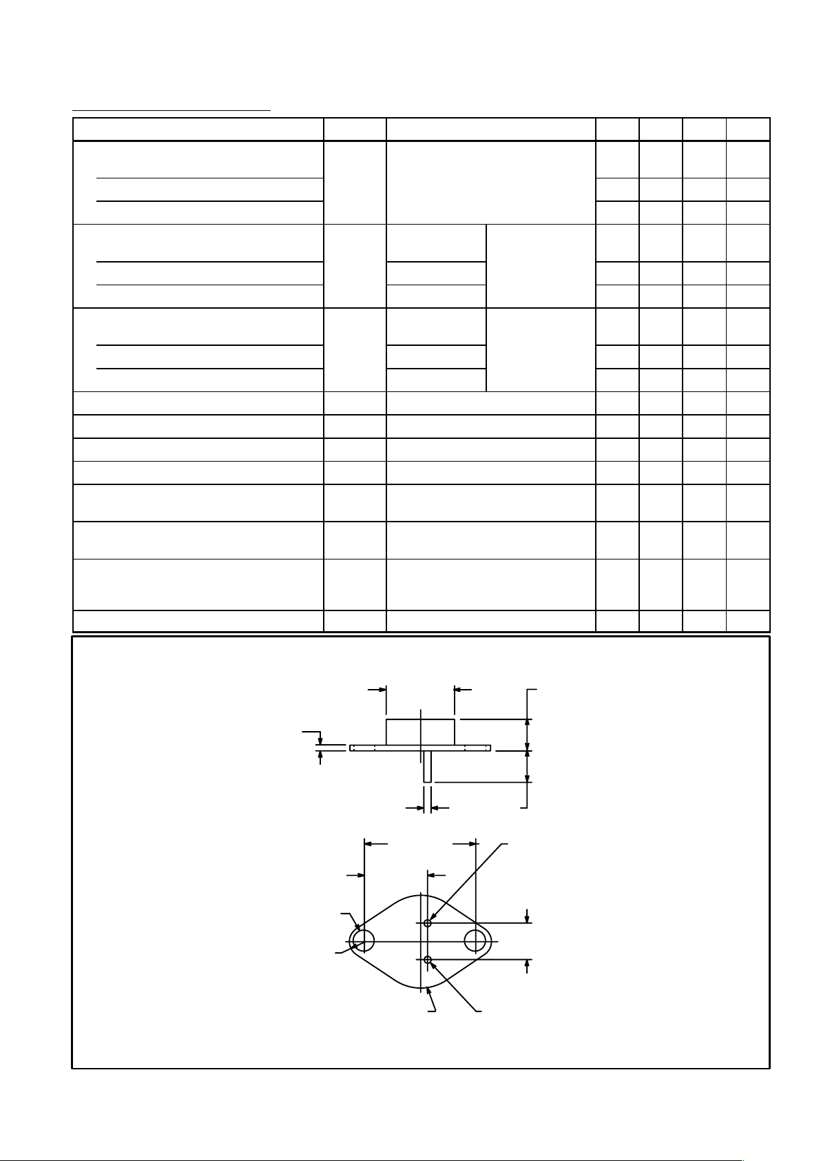
.485 (12.3)
Dia
.062 (1.57)
.295 (7.5)
.360 (9.14)
Min
.031 (0.78) Dia
.960 (24.3) Gate
.580 (14.7)
.200
(5.08)
CathodeAnode/Case
.145 (3.7) R Max
.147 (3.75) Dia
(2 Places)
 Loading...