

NTE NTE5448, NTE5446, NTE5444, NTE5442 Datasheet

NTE5442 thru NTE5448
Silicon Controlled Rectifier (SCR)
8 Amp
Description:
The NTE5442 thru NTE5448 are silicon controlled rectifiers (SCR’s) in a TO127 type package designed for high–volume consumer phase–control applications such as motor speed, temperature,
and light controls, and for fast switching applications in ignition and starting systems, voltage regulators, vending machines, and lamp drivers.
Features:
D Small, Rugged Construction
D Practical Level Triggering and Holding Characteristics @ +25°C:
IGT = 7mA Typ
I
= 6mA Typ
Hold
D Low “ON” Voltage: VTM = 1V Typ @ 5A @ +25°C
D High Surge Current Rating: I
Absolute Maximum Ratings: (Note 1, TJ = +100°C unless otherwise specified)
Peak Repetitive Forward and Reverse Blocking Voltage (Note 2), V
NTE5442 50V. . . . . . . . . . . . . . . . . . . . . . . . . . . . . . . . . . . . . . . . . . . . . . . . . . . . . . . . . . . . . . . . . . . .
NTE5444 200V. . . . . . . . . . . . . . . . . . . . . . . . . . . . . . . . . . . . . . . . . . . . . . . . . . . . . . . . . . . . . . . . . . .
NTE5446 400V. . . . . . . . . . . . . . . . . . . . . . . . . . . . . . . . . . . . . . . . . . . . . . . . . . . . . . . . . . . . . . . . . . .
NTE5448 600V. . . . . . . . . . . . . . . . . . . . . . . . . . . . . . . . . . . . . . . . . . . . . . . . . . . . . . . . . . . . . . . . . . .
Non–Repetitive Peak Reverse Blocking Voltage (t = 5ms (max) duration), V
NTE5442 75V. . . . . . . . . . . . . . . . . . . . . . . . . . . . . . . . . . . . . . . . . . . . . . . . . . . . . . . . . . . . . . . . . . . .
NTE5444 300V. . . . . . . . . . . . . . . . . . . . . . . . . . . . . . . . . . . . . . . . . . . . . . . . . . . . . . . . . . . . . . . . . . .
NTE5446 500V. . . . . . . . . . . . . . . . . . . . . . . . . . . . . . . . . . . . . . . . . . . . . . . . . . . . . . . . . . . . . . . . . . .
NTE5448 700V. . . . . . . . . . . . . . . . . . . . . . . . . . . . . . . . . . . . . . . . . . . . . . . . . . . . . . . . . . . . . . . . . . .
RMS On–State Current (All Conduction Angles), I
Average On–State Current (TC = +73°C), I
Peak Non–Repetitive Surge Current, I
(1/2 cycle, 60Hz preceeded and followed by rated current and voltage) 80A. . . . . . . . . . . . .
Circuit Fusing (TJ = –40° to +100°C, t = 1ms to 8.3ms), I2t 25A2sec. . . . . . . . . . . . . . . . . . . . . . . . . . .
Peak Gate Power, P
Average Gate Power, P
Peak Forward Gate Current, I
GM
G(AV)
GM
Peak Reverse Gate Voltage, V
Operating Junction Temperature Range, T
Storage Temperature Range, T
Maximum Thermal Resistance, Junction–to–Case, R
Typical Thermal Resistance, Junction–to–Ambient, R
Note 1. NTE5444 and NTE5446 are discontinued devices and are replaced by NTE5448.
Note 2. Ratings apply for zero or negative gate voltage but positive gate voltage shall not be applied
concurrently with a negative potential on the anode. When checking forward or reverse
blocking capability, thyristor devices should not be tested with a constant current source in
a manner that the voltage applied exceeds the rated blocking voltage.
TSM
RGM
stg
= 80A
TSM
T(AV)
J
T(RMS)
thJC
thJA
DRM
or V
RRM
RSM
8A. . . . . . . . . . . . . . . . . . . . . . . . . . . . . . . . . .
5.1A. . . . . . . . . . . . . . . . . . . . . . . . . . . . . . . . . . . . . . .
5W. . . . . . . . . . . . . . . . . . . . . . . . . . . . . . . . . . . . . . . . . . . . . . . . . . . . . . . . . . . . .
500mW. . . . . . . . . . . . . . . . . . . . . . . . . . . . . . . . . . . . . . . . . . . . . . . . . . . . . .
2A. . . . . . . . . . . . . . . . . . . . . . . . . . . . . . . . . . . . . . . . . . . . . . . . . . . . . .
10V. . . . . . . . . . . . . . . . . . . . . . . . . . . . . . . . . . . . . . . . . . . . . . . . . . .
–40° to +100°C. . . . . . . . . . . . . . . . . . . . . . . . . . . . . . . . . .
–40° to +150°C. . . . . . . . . . . . . . . . . . . . . . . . . . . . . . . . . . . . . . . . . .
2.5°C/W. . . . . . . . . . . . . . . . . . . . . . . . . . . .
40°C/W. . . . . . . . . . . . . . . . . . . . . . . . . . . . .
Electrical Characteristics: (TC = +25°C unless otherwise specified)
Parameter Symbol Test Conditions Min Typ Max Unit
Peak Forward or Rever se I
Blocking Current
I
Gate Trigger Current
(Continuous DC)
Gate Trigger Voltage
(Continuous DC)
Peak On–State Voltage V
Holding Current I
Gate Controlled Turn–On Time t
Circuit Commutated Turn–Off
Time
Critical Rate–of–Rise of
dv/dt VD = Rate d V
Off–State Voltage
, Rated V
DRM
RRM
I
GT
V
GT
TM
Hold
gt
t
q
or V
DRM
RRM
Gate Open
VD = 7V, RL = 100Ω
,
TJ = +2 5°C – – 10 µA
TJ= +100°C – – 2 mA
TC = +2 5°C – 7 30 mA
TC = –40°C – – 60 mA
VD = 7V, RL = 100Ω TC = +2 5°C – 0.75 1.5 V
TC = –40°C – – 2.5 V
VD = Rate d V
Pulse Width = 1ms to 2 ms,
Duty Cycle ≤ 2%
, RL = 100Ω, TJ = +1 00°C 0.2 – – V
DRM
ITM = 5A
peak
ITM = 15.7A
peak
– 1.0 1.5 V
– – 2.0 V
VD = 7V, Gate Open TC = +2 5°C – 6 40 mA
TC = –40°C – – 70 mA
ITM = 5A, IGT = 20mA, VD = Rate d V
DRM
– 1 – µs
ITM = 5A, IR = 5A – 15 – µs
TJ= +100°C – 20 – µs
, Exponential Waveform,
DRM
– 50 – V/µs
TJ = +1 00°C, Gate Open
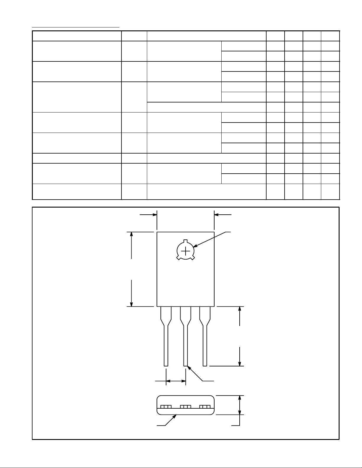
.530 (13.4) Max
.668
(17.0)
Max
.166 (4.23)
.143 (3.65) Dia Thru
KG
.655
(16.6)
Max
A (Heat Sink Area)
Area (Bottom)
.150 (3.82) MaxHeat Sink Contact
 Loading...