


NTE5424
Silicon Controlled Rectifier (SCR)
for TV Power Supply Switching
Description:
The NTE5424 is a silicon controlled rectifier (SCR) in a TO220 type package designed for high–speed
switching applications such as power inverters, switching regulators, and high–current pulse applications. This device features fast turn–off, high dv/dt, and high di/dt characteristics and may be used
at frequencies up to 25kHz.
Features:
D Fast Turn–Off Time
D High di/dt and dv/dt Capabilities
D Shorted–Emitter Gate–Cathode Construction
D Low Thermal Resistance
D Center–Gate Construction
Absolute Maximum Ratings:
Repetitive Peak Off–State Voltage (Gate Open, Note 1), V
Repetitive Peak Reverse Voltage (Gate Open, Note 1), V
RMS On–State Current (TC = +60°C, t1/t2 = 0.5), I
T(RMS)
Average On–State Current (TC = +60°C, t1/t2 = 0.5), I
Peak Surge (Non–Repetitive) On–State Current (One Cycle), I
DRM
RRM
T(AV)
TSM
60Hz Sinusoidal 80A. . . . . . . . . . . . . . . . . . . . . . . . . . . . . . . . . . . . . . . . . . . . . . . . . . . . . . . . . . . . . .
50Hz Sinusoidal 75A. . . . . . . . . . . . . . . . . . . . . . . . . . . . . . . . . . . . . . . . . . . . . . . . . . . . . . . . . . . . . .
Peak Forward Gate Power Dissipation (10µs max, Note 2), P
Peak Reverse Gate Power Dissipation (10µs max, Note 2), P
Average Gate Power Dissipation (10ms max, Note 2), P
GM
RGM
G(AV)
Rate of Change of On–State Current VDM = 400V, IGT = 500mA, tr = 0.5µs), di/dt 200A/µs. . . . . . .
Fusing Current (TC = +60°C, 8.3ms), I2t 26A2s. . . . . . . . . . . . . . . . . . . . . . . . . . . . . . . . . . . . . . . . . . . . .
Operating Case Temperature Range, T
Storage Temperature Range, T
stg
C
Lead Temperature (During Soldering, 10sec max), T
Thermal Resistance, Junction–to–Case, R
thJC
L
–40° to +100°C. . . . . . . . . . . . . . . . . . . . . . . . . . . . . . . . . . . .
–40° to +150°C. . . . . . . . . . . . . . . . . . . . . . . . . . . . . . . . . . . . . . . . . .
400V. . . . . . . . . . . . . . . . . . . . . . . . . .
400V. . . . . . . . . . . . . . . . . . . . . . . . . . .
5.0A. . . . . . . . . . . . . . . . . . . . . . . . . . . . . . .
3.2A. . . . . . . . . . . . . . . . . . . . . . . . . . . . . .
13W. . . . . . . . . . . . . . . . . . . . . . . .
13W. . . . . . . . . . . . . . . . . . . . . . .
500mW. . . . . . . . . . . . . . . . . . . . . . . . .
+225°C. . . . . . . . . . . . . . . . . . . . . . . . . . . . . . . .
2.2°C/W. . . . . . . . . . . . . . . . . . . . . . . . . . . . . . . . . . . . .
Note 1. These values do not apply if there is a positive gate signal. Gate must be open or negatively
biased.
Note 2. Any product of gate current and gate voltage which results in a gate power less than the max-
imum is permitted.
Electrical Characteristics: (TC = +25°C, “Maximum Ratings” unless otherwise specified)
Parameter Symbol Test Conditions Min Typ Max Unit
Peak Forward Blocking Current I
Peak Reverse Blocking Current I
Forward ON Voltage V
Gate Trigger Current, Continuous DC I
Gate Trigger Voltage, Continuous DC V
DC Holding Current I
Rate of Rise of Off–State Voltage dv/dt VD = 400V, TC = +80°C 100 250 – V/µs
Turn–On Time t
Circuit Commutated Turn–Off Time t
DRM
RRM
TM
GT
GT
gt
VD = 400V, TC = +100°C – 0.5 3.0 mA
VR = 400V, TC = +100°C – 0.3 1.5 mA
ITM = 30A – 2.34 4.0 V
Anode Voltage = 12V, RL = 30Ω – – 50 mA
Anode Voltage = 12V, RL = 30Ω – 1.2 2.5 V
H
VD = 400V, IT = 8A (Peak),
IGT = 300mA, tr = 0.1µs
VD = 400V, Pulse Duration = 50µs,
q
dv/dt = 100V/µs, –di/dt = –10A/µs,
IGT = 100mA at turn–on, IT = 4A,
VGK = 0V at turn–off, TC = +75°C
– 20 50 mA
– 0.7 – µs
– 4.4 – µs
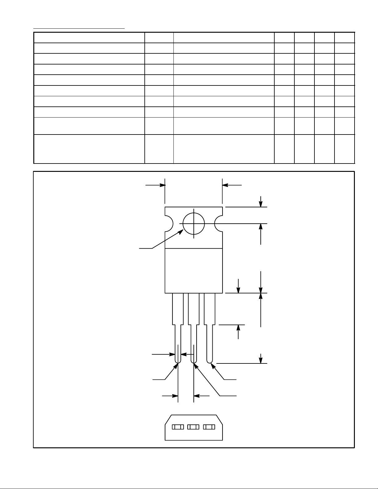
.420 (10.67)
Max
.110 (2.79)
.147 (3.75)
Dia Max
.070 (1.78) Max
Cathode
.100 (2.54) Anode/Tab
.500
(12.7)
Max
.250 (6.35)
Max
.500
(12.7)
Min
Gate
 Loading...