

NTE NTE5409, NTE5408, NTE5410 Datasheet
NTE5408 thru NTE5410
Silicon Controlled Rectifier (SCR)
3 Amp Sensitive Gate
Description:
The NTE5408 through NTE5410 sensitive gate SCRs are designed to be driven directly with IC and
MOS devices. These SCRs feature proprietary, void–free glass–passivated chips and are hermetically sealed in TO5 type packages. These 4A devices are available in voltages up to 600V and with
a gate current of 200µA.
These NTE SCRs are reverse–blocking triode thyristors and may be switched from off–state to conduction by a current pulse applied to the gate terminal. The NTE5408 through NTE5410 are designed
for control applications in lighting, heating, cooling, and static switching relays.
Absolute Maximum Ratings:
Repetitive Peak Reverse Voltage (TC = +100°C), V
RRM
NTE5408 200V. . . . . . . . . . . . . . . . . . . . . . . . . . . . . . . . . . . . . . . . . . . . . . . . . . . . . . . . . . . . . . . . . . .
NTE5409 400V. . . . . . . . . . . . . . . . . . . . . . . . . . . . . . . . . . . . . . . . . . . . . . . . . . . . . . . . . . . . . . . . . . .
NTE5410 600V. . . . . . . . . . . . . . . . . . . . . . . . . . . . . . . . . . . . . . . . . . . . . . . . . . . . . . . . . . . . . . . . . . .
Repetitive Peak Off–State Voltage (T
C
= +100°C), V
DRXM
NTE5408 200V. . . . . . . . . . . . . . . . . . . . . . . . . . . . . . . . . . . . . . . . . . . . . . . . . . . . . . . . . . . . . . . . . . .
NTE5409 400V. . . . . . . . . . . . . . . . . . . . . . . . . . . . . . . . . . . . . . . . . . . . . . . . . . . . . . . . . . . . . . . . . . .
NTE5410 600V. . . . . . . . . . . . . . . . . . . . . . . . . . . . . . . . . . . . . . . . . . . . . . . . . . . . . . . . . . . . . . . . . . .
RMS On–State Current (T
C
= +75°C, Conduction Angle of 180°), I
T(RMS)
4A. . . . . . . . . . . . . . . . . . .
Peak Surge (Non–Repetitive) On–State Current (One Cycle at 50 or 60Hz), I
TSM
40A. . . . . . . . . . .
Peak Gate–Trigger Current (3µs Max), I
GTM
1A. . . . . . . . . . . . . . . . . . . . . . . . . . . . . . . . . . . . . . . . . . . .
Peak Gate–Power Dissipation (I
GT
≤ I
GTM
for 3µs Max), P
GM
20W. . . . . . . . . . . . . . . . . . . . . . . . . . .
Average Gate Power Dissipation, P
G(AV)
200mW. . . . . . . . . . . . . . . . . . . . . . . . . . . . . . . . . . . . . . . . . .
Operating Temperature Range, T
opr
–40° to +100°C. . . . . . . . . . . . . . . . . . . . . . . . . . . . . . . . . . . . . . . .
Storage Temperature Range, T
stg
–40° to +150°C. . . . . . . . . . . . . . . . . . . . . . . . . . . . . . . . . . . . . . . . . .
Typical Thermal Resistance, Junction–to–Case, R
thJC
+5°C/W. . . . . . . . . . . . . . . . . . . . . . . . . . . . . .
Electrical Characteristics: (TC = +25°C unless otherwise specified)
Parameter Symbol Test Conditions Min Typ Max Unit
Peak Off–State Current
I
RRM
V
RRM
= Max, V
DRXM
= Max,
– – 0.75 mA
I
DRXM
TC = +100°C, RGK = 1kΩ
– – 0.75 mA
Maximum On–State Voltage V
TM
IT = 10A (Peak) – – 2.2 V
DC Holding Current I
HOLD
RGK = 1000Ω – – 5 mA
DC Gate–Trigger Current I
GT
VD = 6VDC, RL = 100Ω – – 200 µA
DC Gate–Trigger Voltage V
GT
VD = 6VDC, RL = 100Ω – – 0.8 V
Gate Controlled Turn–On Time t
gt
IG x 3
GT
– 1.2 – µs
I2t for Fusing Reference I2t For SCR Protection – – 2.6 A2sec
Critical Rate of Applied
Forward Voltage
dv/dt
(critical)
RGK = 1kΩ, TC = +100°C – 5 – V/µs
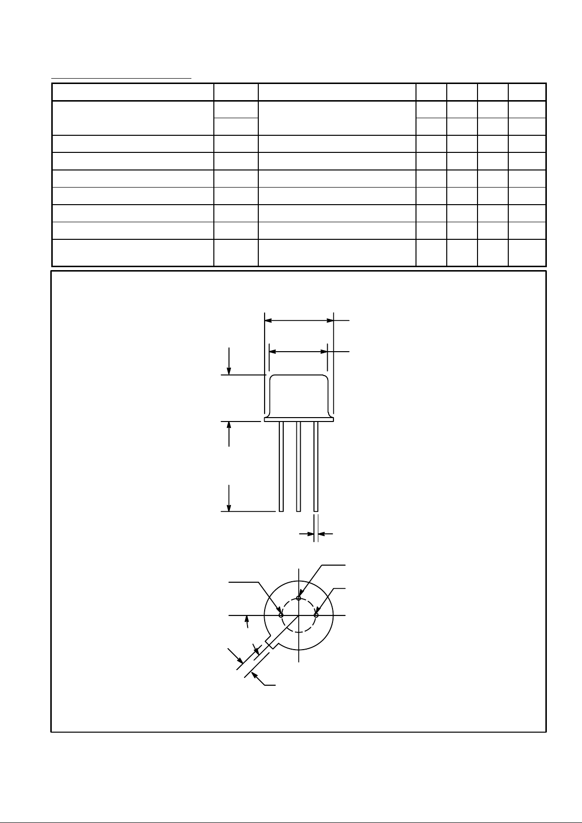
.250
(6.35)
Max
.500
(12.7)
Min
.352 (8.95) Dia Max
.325 (8.13) Dia Max
45°
.031 (.793)
Cathode
Gate
Anode
.019 (0.5)
 Loading...