

TL/F/12147
PCM16C010 Configurable PC Card Interface Chip
August 1996
PCM16C010
Configurable PC Card Interface Chip
General Description
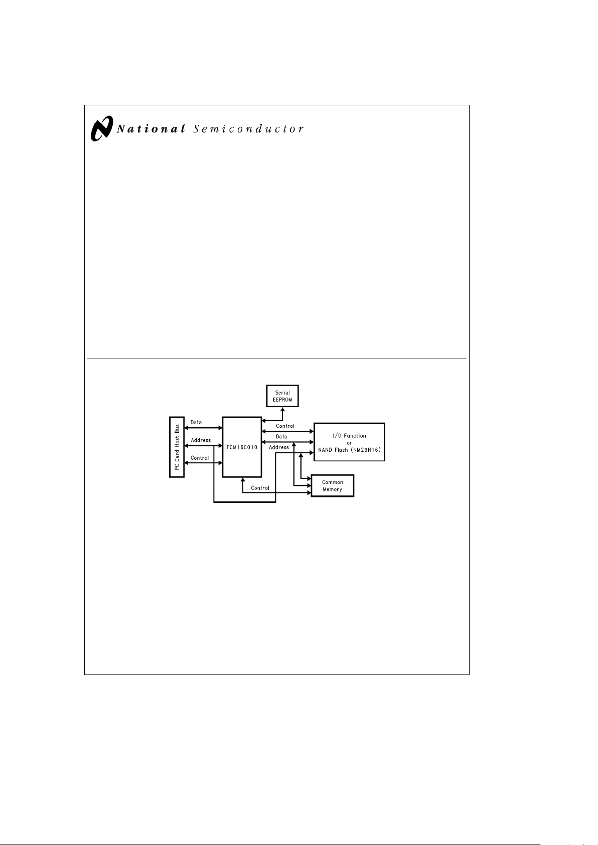
National’s PCM16C010 acts as a standard interface between the PC Card Host bus and local card busses found on
I/O and memory PC Cards. This device allows the card designer to focus on the design of the I/O functions while
providing a one-chip solution for I/O memory window control, EEPROM interfacing, and power management.
The PCM16C010 provides a PC Card interface for any ISA
like function which allows it to be placed on a PC Card.
In addition, the PCM16C010 provides the capability to configure the function as a NAND Flash (NM29N16) interface;
supporting all of the necessary control signals required to
handshake with NAND Flash (NM29N16) memory devices.
The PCM16C010 is fully compliant with the PC Card Standard. This IC allows the system software to setup an I/O
decode window and provides the Attribute memory decode
control that allow attribute read and write data transfers.
Note, PC Card refers to technology developed to the PC
Card Standards determined by the PCMCIA Standards
Committee.
Features
Y
PC Card bus interface
Y
PC Card Standard configuration registers
Y
100 pin TQFP package
Y
Configurable as NAND Flash (NM29N16) interface
Y
Serial EEPROM Interface compatible with
MICROWIRE
TM
EEPROM protocol
Y
1-kbyte on chip RAM for attribute memory which shadows the CIS and is used for loading static registers
Y
Address decoding and control for I/O functions
Y
Power management and clock control
Y
Common memory logic for common memory devices including NOR Flash devices
Y
Operating voltage rangeeVCC(opr)e3VE5.0V
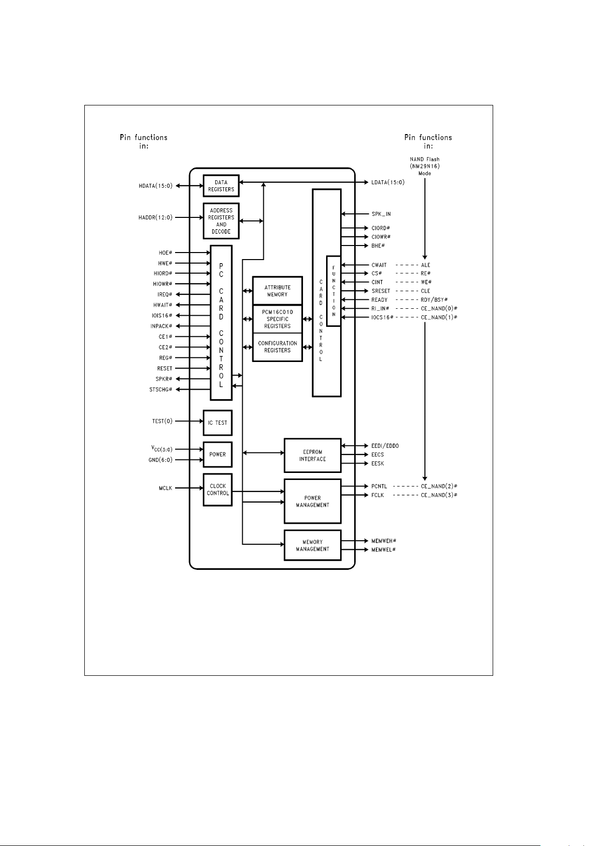
1.0 System Diagram
TL/F/12147– 1
FIGURE 1-1
TRI-STATEÉis a registered trademark of National Semiconductor Corporation.
MICROWIRE
TM
is a trademark of National Semiconductor Corporation.
C
1996 National Semiconductor Corporation RRD-B30M17/Printed in U. S. A.
http://www.national.com

Table of Contents
GENERAL DESCRIPTION AND PRODUCT FEATURES АААААААААААААААААААААААААААААААААААААААААААААААААААААААААААА 1
1.0 SYSTEM DIAGRAM АААААААААААААААААААААААААААААААААААААААААААААААААААААААААААААААААААААААААААААААААААААААА 1
2.0 CONNECTION DIAGRAM ААААААААААААААААААААААААААААААААААААААААААААААААААААААААААААААААААААААААААААААААААА 3
3.0 PINOUT DESCRIPTION AND DETAILED TABLES ААААААААААААААААААААААААААААААААААААААААААААААААААААААААААААА 4
4.0 BLOCK DIAGRAM ААААААААААААААААААААААААААААААААААААААААААААААААААААААААААААААААААААААААААААААААААААААААА 7
5.0 FUNCTIONAL DESCRIPTION ААААААААААААААААААААААААААААААААААААААААААААААААААААААААААААААААААААААААААААААА 8
5.1 Address Maps АААААААААААААААААААААААААААААААААААААААААААААААААААААААААААААААААААААААААААААААААААААААААААА 8
5.1.1 Attribute Memory Addressing ААААААААААААААААААААААААААААААААААААААААААААААААААААААААААААААААААААААААА 8
5.1.2 I/O Memory Addressing АААААААААААААААААААААААААААААААААААААААААААААААААААААААААААААААААААААААААААААА 9
5.1.3 Common Memory Addressing ААААААААААААААААААААААААААААААААААААААААААААААААААААААААААААААААААААААААА 9
5.2 CIS (Card Information Structure) АААААААААААААААААААААААААААААААААААААААААААААААААААААААААААААААААААААААААААА 9
5.3 Registers АААААААААААААААААААААААААААААААААААААААААААААААААААААААААААААААААААААААААААААААААААААААААААААААА 9
5.3.1 PCM16C010 Specific Registers ААААААААААААААААААААААААААААААААААААААААААААААААААААААААААААААААААААААА 9
5.3.2 PC Card Register АААААААААААААААААААААААААААААААААААААААААААААААААААААААААААААААААААААААААААААААААААА11
5.4 Logic Descriptions АААААААААААААААААААААААААААААААААААААААААААААААААААААААААААААААААААААААААААААААААААААААА14
5.4.1 I/O Card Interface Logic for PC Card Host I/O Access ААААААААААААААААААААААААААААААААААААААААААААААААААА14
5.4.2 EEPROM Interface АААААААААААААААААААААААААААААААААААААААААААААААААААААААААААААААААААААААААААААААААА14
5.4.3 Power Management ААААААААААААААААААААААААААААААААААААААААААААААААААААААААААААААААААААААААААААААААА15
5.4.4 NAND Flash (NM29N16) Interface ААААААААААААААААААААААААААААААААААААААААААААААААААААААААААААААААААААА15
NAND Flash (NM29N16) Mode Register Set (Table 5-2) АААААААААААААААААААААААААААААААААААААААААААААААААА16
NAND Flash (NM29N16) Interface Block Diagram
(Figure 5-2)
ААААААААААААААААААААААААААААААААААААААААААААА17
Typical PCM16C010 to NAND Flash (NM29N16) Read to I/O Space Sequence (
Figures 5-3, 5-4
and Table 5-3) À18
6.0 OPERATIONAL MODES АААААААААААААААААААААААААААААААААААААААААААААААААААААААААААААААААААААААААААААААААААА20
6.1 Initial Setup (Reset) and Configuration ААААААААААААААААААААААААААААААААААААААААААААААААААААААААААААААААААААААА20
6.2 Reset Conditions ААААААААААААААААААААААААААААААААААААААААААААААААААААААААААААААААААААААААААААААААААААААААА20
6.3 16-Bit/8-Bit Operation ААААААААААААААААААААААААААААААААААААААААААААААААААААААААААААААААААААААААААААААААААААА20
6.4 Special Testability Modes АААААААААААААААААААААААААААААААААААААААААААААААААААААААААААААААААААААААААААААААААА20
SOFTWARE ААААААААААААААААААААААААААААААААААААААААААААААААААААААААААААААААААААААААААААААААААААААААААААААААААА20
ABSOLUTE MAXIMUM RATINGSАААААААААААААААААААААААААААААААААААААААААААААААААААААААААААААААААААААААААААААААА21
RECOMMENDED OPERATING CONDITIONS ААААААААААААААААААААААААААААААААААААААААААААААААААААААААААААААААААААА21
RELIABILITY REQUIREMENTS ААААААААААААААААААААААААААААААААААААААААААААААААААААААААААААААААААААААААААААААААА21
DC ELECTRICAL CHARACTERISTICS ААААААААААААААААААААААААААААААААААААААААААААААААААААААААААААААААААААААААААА21
TIMING SPECIFICATIONS AND DIAGRAMS АААААААААААААААААААААААААААААААААААААААААААААААААААААААААААААААААААААА23
CAPACITANCE АААААААААААААААААААААААААААААААААААААААААААААААААААААААААААААААААААААААААААААААААААААААААААААААА37
TYPICAL APPLICATIONS АААААААААААААААААААААААААААААААААААААААААААААААААААААААААААААААААААААААААААААААААААААА37
REFERENCES ААААААААААААААААААААААААААААААААААААААААААААААААААААААААААААААААААААААААААААААААААААААААААААААААА37
PHYSICAL DIMENSIONS ААААААААААААААААААААААААААААААААААААААААААААААААААААААААААААААААААААААААААААААААААААААА38
http://www.national.com 2
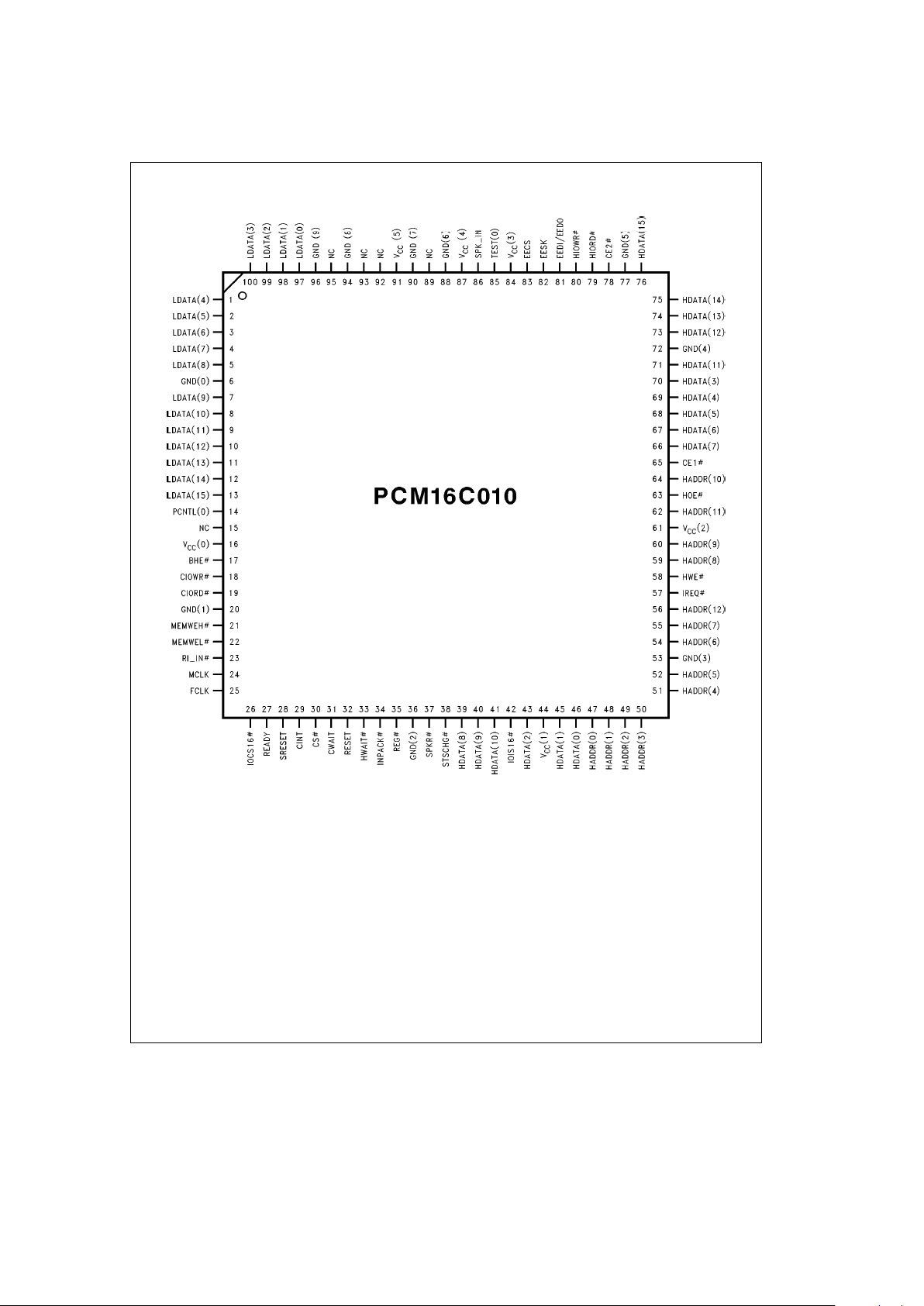
2.0 Connection Diagram
TL/F/12147– 2
NCeNo Connect
Order Number PCM16C010VJG
See NSC Package Number VJG100A
http://www.national.com3

3.0 Pinout Description
TABLE 3-1. PC Card Host-Side Pins
Pin Pin Pin Level Internal
Description
Name Type No. Compatibility Resistor
HDATA(15:0) I/O 39–41, 43, 45, TTL 6 mA
l
100k to GND PC Card Host Data Bus.
46, 66–71, 73 –76
HADDR(12:0) I 47 –52, 54 – 56, TTL
l
100k to GND PC Card Host Address Bus.
59, 60, 62, 64
HOE
Ý
I 63 TTL
l
100k to V
CC
PC Card Host uses this pin to read
common or attribute memory space.
HWE
Ý
I 58 TTL
l
100k to V
CC
PC Card Host uses this pin to write
common or attribute memory space.
HIORD
Ý
I 79 TTL
l
100k to V
CC
PC Card Host uses this pin to read I/O
memory space.
HIOWR
Ý
I 80 TTL
l
100k to V
CC
PC Card Host uses this pin to write I/O
memory space.
IREQ
Ý
O 57 CMOS 6 mA Interrupt Request signal to PC Card Host.
HWAIT
Ý
O 33 CMOS 6 mA This pin allows the PCM16C02 to insert
wait states in a PC Card transaction.
IOIS16
Ý
O 42 CMOS 6 mA Low indicates this I/O access to the card
is capable of 16-bit access. The Function
may use IOCS16Ýto control this signal
and inform the host if a 16-bit access to
the target is feasible.
INPACK
Ý
O 34 CMOS 6 mA Signals a valid I/O read.
CE1
Ý
I 65 TTL
l
100k to V
CC
Indicates even address byte. Odd
addresses are not released. CE1
Ý
and
CE2
Ý
assertion encodings are specified
by the PC Card Standard.
CE2
Ý
I 78 TTL
l
100k to V
CC
Indicates odd addressing only. CE1Ýand
CE2
Ý
assertion encodings are specified
by the PC Card Standard.
REG
Ý
I 35 TTL
l
100k to V
CC
Indicates access to attribute memory
space or I/O address space. REG
Ý
must
be high to access common memory
space.
RESET I 32 TTL Schmitt
l
100k to V
CC
Asynchronously resets the PCM16C02.
SPKR
Ý
O 37 CMOS 6 mA If Audio bits are set in the Card
Configuration Status Register and in the
Function Configuration Status Register
then SPKR
Ý
is invert of SPKÐIN pin,
else SPKR
Ý
is high.
STSCHG
Ý
O 38 CMOS 6 mA STSCHGÝis asserted when the
Changed bit and SigChg bit are set in the
Card Configuration Status Register.
http://www.national.com 4
3.0 Pinout Description (Continued)
TABLE 3-2. Serial EEPROM Interface Pins
Pin Pin Pin Level Internal
Description
Name Type No. Compatibility Resistor
EEDI/EEDO I/O 81 TTL 6 mA Serial Data in to/from EEPROM.
EECS O 83 CMOS 6 mA EEPROM Chip Select.
EESK O 82 CMOS 6 mA EEPROM Clock. FreqeMCLK(0)/32.
Note: The Enable EEPROM function is performed in software by writing to the EEPROM Control Register. The Enable EEPROM bit will default to low (disabled)
upon power on.
TABLE 3-3. Card-Side Interface Pins
Pin Pin Pin Level Internal
Description
Name Type No. Compatibility Resistor
LDATA(15:0) I/O 1– 5, 7 –13, TTL 6 mA Hold Circuit Card-side Data Bus.
97–100 (Note 1)
SPKÐIN I 86 TTL Schmitt Input Audio Signal.
RIÐIN
Ý
I (Note 2) 23 TTL Schmitt Ring Indicator for function 0.
CIORD
Ý
O 19 CMOS 6 mA I/O read signals are passed through from HIORD
Ý
according to the expression shown below when a
valid address is decoded.
CIORD
Ý
e
HIORD
Ý
a
REG
Ý
a
(CE1Ý* CE2Ý)
CIOWR
Ý
O 18 CMOS 6 mA I/O write signals are passed through from HIOWR
Ý
according to the expression shown below when a
valid address is decoded.
CIOWR
Ý
e
HIOWR
Ý
a
REG
Ý
a
(CE1Ý* CE2Ý)
CWAIT I (Note 2) 31 TTL Card-side transaction wait state input.
CS
Ý
O 30 CMOS 6 mA Chip select for function.
BHE
Ý
O 17 CMOS 6 mA Byte high enable. When de-asserted and CS( )
Ý
asserted, an 8-bit access on LDATA(7:0) is in
progress. This holds for both odd and even
addresses. When asserted and CS( )
Ý
asserted, a
16-bit access on LDATA(15:0) is in progress.
READY I 27 TTL
l
100k to VCCIndicates that the function is either READY or
E
READY (i.e. - Busy). This signal is used to assert
the Rdy/Bsy
Ý
bit in Pin Replacement Registers.
CINT I (Note 2) 29 TTL Schmitt Card-side interrupt input signal.
SRESET O 28 CMOS 6 mA Signals reset to Card-side function.
IOCS16
Ý
I (Note 2) 26 TTL This pin is asserted during an access to a function if
that function is capable of a 16-bit access.
PCNTL O 14 CMOS 6 mA Power management control signals or general
output.
MCLK I 24 TTL Schmitt Input clock for function.
FCLK O 25 CMOS 6 mA Output clock signal for function. This may be gated
on/off or be a divided value of MCLK.
MEMWEH
Ý
O Tri 21 CMOS 6 mA
l
10k to V
CC
Common Memory write output for upper byte of data
word.
MEMWEL
Ý
O Tri 22 CMOS 6 mA
l
10k to V
CC
Common Memory write output for lower byte of data
word.
Note 1: The Hold Circuit will hold the signal to the logic value it was last set to when the line is TRI-STATEÉ. This will insure that inputs do not float during a
TRI-STATE condition.
Note 2: The CWAIT, CINT, RIÐIN and IOCS16
Ý
pins are outputs (O) when the function is configured for the NAND Flash (NM29N16) Mode.
http://www.national.com5
3.0 Pinout Description (Continued)
TABLE 3-4. Miscellaneous Pins
Pin Pin Pin Level Internal
Description
Name Type No. Compatibility Resistor
TEST(0) I 85 TTL
l
100k to GND Test pin. This pin should be left disconnected for
normal operation.
VCC(5:0) Power 84, 61, 44, Power Voltage.
16, 87, 91
GND(9:0) Power 88, 77, 72, Return Voltage.
53, 36, 20, 6,
90, 94, 96
TABLE 3-5. NAND Flash (NM29N16) Mode Pins
Pin Pin Pin Level Internal
Description
Name Type No. Compatibility Resistor
ALE O 31 CMOS 6 mA Address Latch Enable
(Note 1)
CLE O 28 CMOS 6 mA Command Latch Enable
WE
Ý
O 29 CMOS 6 mA Write Enable
(Note 1)
RE
Ý
O 30 CMOS 6 mA Read Enable
RDY/BSY
Ý
I 27 TTL
l
100k to VCCReady/Busy Input
CEÐNAND (3:0)
Ý
O 23, 26, CMOS 6 mA Chip Enables for NAND Flash (NM29N16) Devices
(Note 1) 14, 25
Note 1: The ALE, WEÝ,CEÐNAND(0)Ý, and CEÐNAND(1)Ýpins are inputs (I) when function 0 is NOT configured for the NAND Flash (NM29N16) Mode.
Pin Total:
Host-Side Interface Pins 44
EEPROM Interface Pins 4
Card-Side Interface Pins 30
Miscellaneous Pins 22
Total Pins 100
http://www.national.com 6
4.0 Block Diagram
TL/F/12147– 3
FIGURE 4-1
http://www.national.com7

5.0 Functional Description
The PCM16C02 provides an integrated solution to interfacing dual function I/O cards with the PC Card Bus. The part
has a contiguous 1-kbyte RAM block to store attribute memory. The IC also provides an EEPROM interface to serial
EEPROMs that use the MICROWIRE protocol. At a minimum, a 16-kbit serial EEPROM is required. The part allows
I/O address windows to be programmed independently for
each function.
5.1 ADDRESS MAPS
5.1.1 Attribute Memory Addressing
The Attribute Memory space contains both the Card Information Structure (CIS), PC Card Registers for both I/O functions, and PCM16C02 implementation specific registers.
Note that PC Card Standard specifies that Attribute memory
may only be accessed on even address byte boundaries.
The Attribute Memory space fragmentation is shown in Table 5-1.
TABLE 5-1. Attribute Memory Map
Register Description Register Type Address (Hex) EEPROM
Card Information Structure PC Card CIS 0x000–0x03E2 Yes
Pin Polarity Register PCM16C02 Specific 0x03E4 Yes
PMGR and Clock Register PCM16C02 Specific 0x03E6 Yes
CTERM Register PCM16C02 Specific 0x03E8 Yes
Unused PCM16C02 Specific 0x03EA Yes
Reserved for Future Use Registers PCM16C02 Specific 0x03EC –0x03EE Yes
Miscellaneous Register PCM16C02 Specific 0x03F0 Yes
Reserved for Future Use Registers PCM16C02 Specific 0x03F2 –0x03F4 Yes
Wait State Timer Registers PCM16C02 Specific 0x03F6 Yes
NAND Flash (NM29N16) Config Register PCM16C02 Specific 0x03F8 Yes
Reserved for Future Use Register PCM16C02 Specific 0x03FA Yes
Watchdog Timer Register PCM16C02 Specific 0x03FC Yes
Reserved for Future Use Registers PCM16C02 Specific 0x03FE Yes
Card Information Structure PC Card CIS 0x0400– 0x07FE Optional
ID Register PCM16C02 Specific 0x1000 No
EEPROM Control Register PCM16C02 Specific 0x1002 No
EEPROM Security Register PCM16C02 Specific 0x1004 No
Reserved for Future Use Registers PCM16C02 Specific 0x1006 –0x101E No
Function Configuration Option Register PC Card 0x1020 No
Function Configuration Status Register PC Card 0x1022 No
Function Pin Replacement Register PC Card 0x1024 No
Unused PC Card 0x1026 No
Function I/O Event Register PC Card 0x1028 No
Function Base A Register PC Card Extension 0x102A No
Function Base B Register PC Card Extension 0x102C No
Unused PC Card Extension 0x102E –0x1030 No
Function Limit Register PC Card Extension 0x1032 No
Reserved for Future Use Registers PC Card Extension 0x1034 –0x103E No
Reserved for Future Use Registers PC Card Extension 0x1040 –0x105E No
http://www.national.com 8
5.0 Functional Description (Continued)
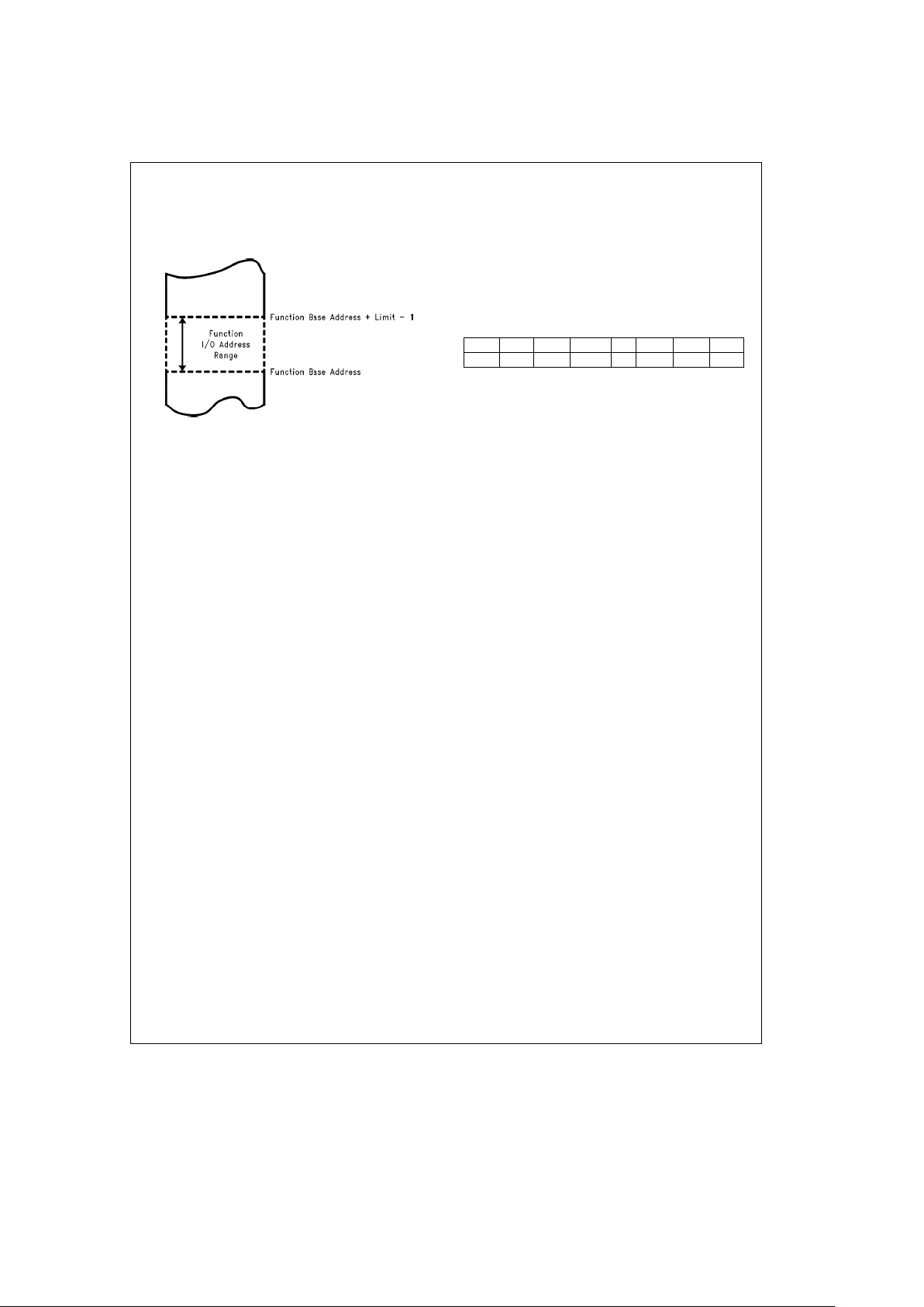
5.1.2 I/O Memory Addressing
National’s PCM16C010 uses address base and limit registers to steer I/O transactions from the PC Card Host to the
card function.
TL/F/12147– 4
I/O Address Space
FIGURE 5-1. I/O Address Decoding for
Two Functions on a PC Card
5.1.3 Common Memory Addressing
The NSC PCM16C010 does not specifically decode common memory address accesses initiated by the host. Rather, it will pass a host access of HDATA(15:0) through to
LDATA(15:0) while passing the address lines around the
PCM16C010. In addition, PCM16C010 will pass the host
HWE
Ý
signal assertion to the MEMWEHÝ/
MEMWEL
Ý
signals appropriately based upon the proper
assertion of CE1
Ý
, CE2Ý, and REGÝ. The assertion of
MEMWEH
Ý
, MEMWELÝ, or both is determined by an 8-bit
or 16-bit access as specified in the PC Card Standard.
If a function is mapped to common memory, and requires
further address lines, it may use the HADDR(25:13) lines
from the PC Card socket as additional address lines around
the PCM16C010. The card design is free to use external
decoding logic for common memory.
5.2 CIS (CARD INFORMATION STRUCTURE)
[
0x000–0x03E2
]
When the PCM16C010 powers on, the contents of the lower
1-kbyte of the EEPROM are loaded into the device’s shadow RAM. This not only allows attribute memory accesses to
the CIS, but, it also provides defaults for 9 PCM16C010 specific registers to be loaded. This allows default loading of
parameters that are transparent to system or device software. The best use is for the card manufacturer to determine what values these should be and program them into
the EEPROM when the CIS is programmed. Either system
software such as Card Services/Socket Services or device
software may read and parse the CIS by accessing attribute
memory on the PC Card. If desired, this software agent may
write to the CIS or default EEPROM registers and, if desired,
have these new values saved to the EEPROM. The actual
contents of the CIS and the static registers is PC Card design dependent.
5.3 REGISTERS
5.3.1 PCM16C010 Specific Registers
These registers are defined specifically for National’s
PCM16C010 IC, allowing the PCM16C010 to perform its
base functionality. These registers are not part of the PC
Card Standard.
Pin Polarity Register
[
0x03E4
]
This register sets the polarity of the card side interface signals.
D7 D6 D5 D4 D3 D2 D1 D0
CIOWR CIORD Unused SRESET BHE Memls8 Unused CWAIT
CIOWR, CIORDÐSets the polarity of the CIOWRÝand
CIORD
Ý
pins respectively. A high indicates active high. The
default polarity is active-low.
SRESETÐSets the polarity of the SRESET pin. When this
bit is set to a zero (0), the output signal is asserted in the
high (1) state. When this bit is set to a one (1), the output
signal is asserted in the low (0) state. The bit default is zero
(0), i.e. the SRESET signal is active high.
BHEÐSets the polarity of the BHE
Ý
pin. A high indicates
active-high. The default polarity is active-low.
Memls8ÐThis bit is set to one (1) if common memory is
organized for 8-bit access. This bit is set to zero (0) if common memory is organized for 16-bit access. The default value is zero (0). This information allows the PCM16C010 to
properly access memory using the MEMWEH
Ý
, and
MEMWEL
Ý
, signals.
CWAITÐWhen this bit is set to one (1), the PCM16C010
interprets this input signal active when it is low (0). When
this bit is set to zero (0), the PCM16C010 interprets this
input signal as active when it is high (1). The default bit
value is zero (0), i.e. the CWAIT input signal is asserted high
(1).
UnusedÐThese bits are not used for operation of the
PCM16C010. These bits must be set to zero (0) in the CIS
for initialization and must not be changed from zero (0) to
ensure proper operation of the card.
PMGR and Clock Register
[
0x03E6
]
The Power Manager (PMGR) and Clock Register is used for
controlling the PCNTL and FCLK pins for power management purposes.
Hardware power management is enabled using the Function Configuration Option Register’s PMGMTÐEN(D3) bit.
Its use is intended for functions that can be sequenced on/
off or into idle or sleep states with a quick (
k
10 ms) response time when powered on again. That is, the function
may use its CWAIT signal to extend a transaction that
caused the PCM16C010 to turn it on. Use of the READY
signal in a dynamic hardware power managed environment
to set the RRdy/Bsy bits in order to achieve
l
10 ms response times for power on is not guaranteed to work since
system software may not inspect the RRdy/Bsy bit in all
such instances.
http://www.national.com9
5.0 Functional Description (Continued)
D7 D6 D5 D4 D3 D2 D1 D0
Unused Unused Unused Unused FCLKEN DIV PPOL PCNTL
FCLKENÐIf set, these enable the FCLK pin to receive a
clock out. If clear, FCLK will be forced low. These are set
and cleared by software if desired or statically loaded upon
card power up from the EEPROM.
DIVÐIf set, the respective clock output from FCLK will be
divided by 32 from the input clocks MCLK. If clear, the clock
output FCLK will equal the respective clock input MCLK.
These are set and cleared by software if desired or statically
loaded upon card power up from the EEPROM.
PPOLÐSets the active polarity of the PCNTL signal such
that the function is asserted. If PPOL is set to zero (0),
PCNTL is asserted when in the high state. If set to one (1),
PCNTL is asserted when in the low state. The default is set
to zero (0), i.e. PCNTL defaults to active high.
PCNTLÐThis bit controls the PCNTL Pin. If hardware power management is not selected in the Function Configuration Option Register’s Function Configuration Index, then
this bit may be used as an output signal by software for
general purposes. If the hardware power management configuration is selected, this bit is de-asserted (defined by
PPOL) when the PCM16C010’s CTERM counter expires.
This bit will be asserted if a transaction occurs to the function through an I/O window or the function requests service
by issuing a RIÐIN( ). In either strategy, software may always write and read back these bits. This bit defaults to zero
(0) during power-on until the PMGR and Clock Register can
be loaded from the EEPROM.
UnusedÐThese bits are not used for operation of the
PCM16C010. These bits must be set to zero (0) in the CIS
for initialization and must not be changed from zero (0) to
insure proper operation of the card.
CTERM Register
[
0x03E8
]
This register is used to define the value of the function’s
power time-out counter. If the function’s power time-out
counter expires, the PCNTL bit for the function in the PMGR
and Clock Register is de-asserted. This will occur if a function is in-active long enough for it’s power time-out counter
to expire. Active is defined as having either an I/O access
from the host or receiving a RIÐIN( )
Ý
. Devices that may
operate for long periods of time without a host I/O access
should follow a software controlled power management
strategy that uses the PwrDn bits in the Function Configuration Status Register.
D7–D0
NeTime-Out Counter Terminal Count Value
The function’s terminal counter is 8 bits wide and counts at
a rate of MCLK(0)/(2
17
). For example, if the MCLK frequency is 30 MHz the device can be programmed to time-out
between 0.0s to 1.114s. The general formula is:
Time
e
(1/mclk) * 217* N,
where NeÀ0, 1, 2, . . . , 255
Ó
For a 5 MHz MCLK frequency, the equation is:
TimeeN (26.2144 ms) where NeÀ0,1,2, . . . ,255
Ó
Note: A value of zero implies the function is powered down.
Miscellaneous Register
[
0x03F0
]
D7 D6 D5 D4 –D0
FastEE RFU RFU EEPROMStartAddr
FastEEÐIf this bit is set to one (1), then the clock used to
access the EEPROM shall be MCLK/2. If this bit is set to
zero (0), the clock used to access the EEPROM shall be
MCLK/32.
EEPROMStartAddrÐThis field contains a starting address
for EEPROM read or write access. This is ordinarily set to
zero and is used for debug/test purposes.
Wait State Timer Register
[
0x03F6
]
This register allows the insertion of default wait states from
the PCM16C010 using HWAIT
Ý
. It is intended to be used in
situations where either the function is too slow to respond
with a CWAIT or the unique wait timing constraints between
the system and PC Card design necessitate a default wait
state.
D7–D4 D3–D2 D1–D0
Reserved Unused Func0Wait
Func0WaitÐThis value is the number (0, 1, 2, or 3) of
MCLK time periods that the PCM16C010 will assert
HWAIT
Ý
during a valid access to a particular function. For
Zero wait states, program this value to 00b.
NAND Flash (NM29N16) Configuration Register[0x03F8
]
D7–D4 D3 D2 D1 D0
Reserved memÐioÐspace NANDÐIOCS16 BC NANDÐEN
memÐioÐspaceÐMemÐioÐspace selects whether
NAND Read/Write strobes are generated by accesses to
common memory space or I/O space. When Function 0 is
configured for NAND Flash (NM29N16) Mode, if memÐio
Ð
space is set to 0, NAND (NM29N16) Read/Write strobes
are generated by an I/O access to the function 0 base address
a
4. If memÐioÐspace is set to 1, Read/Write
strobes are generated by any read/write access to common
memory.
NANDÐIOCS16ÐWhen the Function is configured for
NAND Flash (NM29N16) Mode, D2 replaces the external
pin IOCS16
Ý
to allow the host to know if the NAND
(NM29N16) is organized for 8- or 16-bit accesses. If the
Function is NOT configured for NAND Flash (NM29N16)
Mode, the bit performs no function. This register gets downloaded during EEPROM reads.
BCÐIf set to zero (0), PCM16C010 will assert only one of
the four external CE
Ý
pins at a time, (based on the value of
bits D0 and D1 in the Device Select Register), allowing up to
four unique enable control lines. If set to one (1),
PCM16C010 will place on the external CE
Ý
lines the exact
binary number placed in bits D0 – D3 of the Device Select
Register. This will allow external decoding to produce up to
15 unique CE
Ý
control lines which can control up to 30
pairs of NAND Flash (NM29N16) devices. (Reference table
in Section 5.4.4 for details.)
http://www.national.com 10
5.0 Functional Description (Continued)
NANDÐENÐThis bit, if set to one (1), configures the func-
tion as a NAND Flash (NM29N16) interface (see Section
5.4.4 for specific function details). If set to zero (0), the function assumes normal I/O interface functionality.
Watchdog Time-Out Register
[
0x03FC
]
D7 D6 D5– D0
RFU WaitÐTout Enable RFU
WaitÐTout EnableÐWhen this bit is set to a one (1), the
HWAIT
Ý
time-out watchdog timer is enabled. In addition,
the ability to set
Intr
in the Function Configuration Option
Register,
Intr
in the Card Configuration Register, and
IREQ
Ý
is enabled once the watchdog timer expires. The
watchdog timer may expire if HWAIT
Ý
is asserted for more
than approximately 11.2 ms when MCLK is set to 20 MHz.
This prevents the system from hanging due to prolonged
HWAIT
Ý
assertions. If this bit is reset to zero (0), Wait
Ð
Tout and its associated interrupt capability is disabled during
HWAIT assertions.
ID Register
[
0x1000
]
This read only register provides the software with IC revision
information.
D7–D3 D2–D0
PCM16C010 Codee00010b Revision Codee001b
NSC PCM16C010 CodeÐThis code may be used to identify the NSC PCM16C010 IC. The value of bits D7 –D3 of this
register is 00010, which when appended to the three bits of
the revision code produce: 00010 xxx; which is 1x hex.
Revision CodeÐThis will uniquely identify the silicon version of the PCM16C010 IC as 001b.
EEPROM Access
In order to avoid accidental EEPROM overwrite, the
PCM16C010 utilizes two registers that must be written with
the proper byte sequence in order to enable EEPROM
writes. In order to initiate an EEPROM write, the following
register write sequence must be executed:
Register Attribute Register Address Hex Data
EE Control Reg 1002 2E
EE Security Reg 1004 B7
EE Control Reg 1002 91
Failure to initiate the exact sequence will disable writes
regardless of the value placed in the WriteEEPROM or
EEPROMWriteEn bits of the EEPROM Control Register.
EEPROM Control Register
[
0x1002
]
This register (in conjunction with the EEPROM Security
Register for writes) controls reading and writing the
EEPROM as well as the EEPROM enable.
D7 D6 D5 –D1 D0
WriteEEPROM ReadEEPROM Reserved EEPROMWriteEn
WriteEEPROMÐWhen set, this tells the EEPROM controller to copy the contents of the PCM16C010 Shadow RAM to
the EEPROM, provided the proper write security sequence
listed above has been executed. Once the EEPROM write
has completed, the EEPROM controller clears this bit.
ReadEEPROMÐWhen set, this tells the EEPROM controller to copy the contents of the EEPROM to the shadow
RAM. Once done, the EEPROM controller clears this bit.
Any data modified in the Shadow RAM that has not first
been written back to the EEPROM will be lost. The
EEPROM may be read independent of the value in the
EEPROMWriteEnable bit.
EEPROMWriteEnÐThis must be set to allow EEPROM
writes. If clear, the EEPROM may not be written. The default
value at reset is low. The EEPROM may be read independent of the value of this bit.
Note 1: Upon power-up, the PCM16C010 EEPROM controller copies the
entire contents of the lower 1 kbytes of the EEPROM into the Shadow RAM independent of writing to the EEPROM Control Register.
Note 2: The PCM16C010 EEPROM controller stores data in a 16-bit orga-
nized EEPROM in low/high format. Although Attribute Memory is
on even byte boundaries only, the entire EEPROM’s address space
is used. This eliminates waste of EEPROM memory. Therefore the
Attribute space used by the Shadow RAM is double the actual size
of the EEPROM. For example, if a 16-bit EEPROM is pre-programmed, the low byte at word 0 in the EEPROM will be shadowed
at Attribute location 0x0000 and the high byte will be shadowed at
Attribute location 0x0002. The low byte at EEPROM word 1 will be
shadowed to Attribute location 0x0004, etc.
EEPROM Security Register
[
0x1004
]
This register in conjunction with the EEPROM Control Register is used to prevent accidental EEPROM overwriting.
When written in the proper sequence as outlined above with
hex data B7, it allows EEPROM write access.
5.3.2 PC Card Register
Function Configuration Option Register
[
0x1020
]
D7 D6 D5– D0
SRESET LevIREQ Function Configuration Index
http://www.national.com11

5.0 Functional Description (Continued)
SRESETÐIf the host sets this field to one (1), the
PCM16C010 shall place the given function in the reset
state. When the host returns this field to zero (0), the function shall enter the same unconfigured, reset state as it
does following a power-up and hardware reset. Note that
SRESET does not reset the PCM16C010 thus the Attribute
memory is not reloaded.
LevIREQÐWhen the PCM16C010 is being used as a PC
Card I/O interface and this field is set to one (1), the
PCM16C010 shall generate Level Mode interrupts for the
function using the IREQ
Ý
signal. If the PCM16C010 is being
used as a PC Card I/O interface and this field is set to zero
(0), the PCM16C010 shall generate Pulse Mode interrupts
for the function. Use of Level Mode interrupts is strongly
recommended. The PCM16C010 will also only allow a write
to the LevIREQ bit value to change the interfaces Interrupt
level mode if the given function is configured using
ConfFunc and interrupts are enabled using EnbIREQ.
In addition, the PCM16C010 provides an enhanced interrupt
protocol scheme described by the IntrReset bit in the Function Configuration Status Register. Function configurations
may use Level Mode or Pulse Mode interrupt schemes.
Pulsed Mode interrupt width is given by:
TwidthIREQ
e
16/(FreqMCLK(0))
Using MCLK from 5 MHz – 30 MHz will insure pulse widths
from 0.53 ms –3.2 ms which exceed the 0.5 ms minimum
requirement for the PC Card Standard.
Function Configuration IndexÐWhen the host system
sets this field to the value of the Configuration Entry Number
field of a Configuration Table Entry Tuple, the function shall
enter the configuration described by that tuple. This field
shall be reset to zero (0) by the PCM16C010 when the host
sets the SRESET field to one (1) or the host asserts
RESET. If this field is set to zero (0) explicitly by the host or
implicitly by SRESET or RESET, the function shall use the
Memory Only interface and I/O cycles from the host shall
be ignored by the function.
The following configurations are supported by the Function
Configuration Index.
ConfFunc (D0)ÐIf this is set to one (1), then the PC Card is
configured for that function.
EnbBaseÐLimit (D1)ÐIf this is set to a one (1), the base
and limit register pair for the function is enabled. That is, the
PCM16C010 will only pass I/O transactions whose address
falls within the I/O window specified by the base and limit
pair. If this is set to a zero (0), the PCM16C010 will not test
transactions’ addresses against the base and limit pair for
that function and will, therefore, pass all I/O transactions to
the function. For function operation, the EnbBaseÐLimit
would be enabled for operation with host controllers that
support overlapping windowing and the INPACK
Ý
signal.
For host controllers that do not support INPACK
Ý
but are
capable of windowing granularity required for the function,
EnbBaseÐLimit may be set to zero (0) so that all I/O transactions are passed to the function.
EnbIREQ (D2)ÐWhen the PCM16C010 is being used as a
PC Card I/O interface and this field is set to one (1), the
PCM16C010 shall enable this function to interrupt the host
using the IREQ
Ý
signal. Normally this bit would be set to
one (1). In environments where the function’s software driver will use a polling technique for status information, this bit
could be set to zero (0) to disable interrupts from that function.
PMGMTÐEN (D3)ÐThis bit, if set to a one (1), enables the
hardware power management controller to control the
PCNTL pin for that function. See the PMGR and Clock Register description.
TESTÐMODE(D4)ÐThe TESTÐMODE bit
MUST
be set to
zero (0) for the function to operate in the normal I/O mode
(default state). TESTÐMODE is for NSC factory use only.
Normal card functionallity is not guaranteed in TEST
Ð
MODE.
(D5) is reserved.
Function Configuration Status Register
[
0x1022
]
These PC Card registers are used for function control/
status information.
D7 D6 D5 D4 D3 D2 D1 D0
Changed SigChg IOis8 Reserved Audio PwrDn Intr IntrReset
ChangedÐIf one or more of the state change signals in the
Function Pin Replacement Register are set to one (1), the
PCM16C010 shall set this field to a one (1). If the
PCM16C010 is being operated as a I/O interface, (PC Card
using I/O Interface), and both the Changed and SigChg
fields are set to one (1), the PCM16C010 shall assert the
STSCHG
Ý
signal. If the PC Card, and hence PCM16C010,
is not using the I/O interface, this field is undefined and
ignored.
SigChgÐThis field serves as a gate for asserting the
STSCHG signal. If the PCM16C010 is operated as an I/O
interface, and both the Changed and SigChg fields are set
to one (1), the PCM16C010 shall assert the PC Card
STSCHG
Ý
signal. If the PCM16C010 is operated as an I/O
interface and this field is reset to a zero (0), the
http://www.national.com 12

5.0 Functional Description (Continued)
PCM16C010 shall not assert the STSCHG
Ý
signal. If the
PCM16C010 is not operated as an I/O interface, this field is
undefined and should be ignored.
IOis8ÐWhen the host can only provide I/O cycles with an
8-bit D0–D7 path, the host shall set this bit to a one (1). The
card is guaranteed that accesses to 16-bit registers will occur as two byte accesses rather than a single 16-bit access.
This information is useful when 16-bit and 8-bit registers
overlap.
AudioÐSampling of the signal SPKÐIN and control of
SPKR
Ý
is accomplished using the Audio bit. SPKRÝwill
equate to SPKÐIN
anytime either of the Audio bits is set to
one (1) and the function is configured.
PwrDnÐWhen the host sets this field to one (1), the
PCM16C010 shall set the given function to a power-down
state by de-asserting the PCNTL signal for that function.
While this field is a one (1), the host shall not access the
function on the PC Card. The host shall return this field to
zero (0) before attempting to access the function. The system shall not place the card into a power-down state while
the card’s RDY/BSY
Ý
line is in the low (Busy) state. All
input/output signals particular to the function are
TRI-STATE.
IntrÐIf the function is requesting interrupt servicing (CINT
asserted), the PCM16C010 shall set this field to one (1).
The PCM16C010 shall reset this field to zero (0) when the
interrupt request has been serviced (CINT de-asserted).
IntrResetÐIf IntrReset is set to zero (0), Intr shall be set to
one (1) when an interrupt condition occurs and shall be reset to zero (0) when the interrupt condition has been serviced. A write to the Intr bit will do nothing. If IntrReset is set
to one (1), Intr shall be set to one (1) when an interrupt
condition occurs (CINT pin) and be cleared to a zero (0)
when the interrupt (CINT pin) is serviced, however, a write
of value zero (0) to the FCSR’s Intr bit where IntrReset is set
to one (1) shall cause the PCM16C010 to evaluate the CINT
signal and generate another interrupt to the system if an
interrupt is pending. Note that the write of zero (0) to
FCSR’s Intr bit where IntrReset is set to one (1) is an indication to the PCM16C010 that it must evaluate CINT and generate a specified pulse to the system on the IREQ line. This
protocol will work in either pulse or level mode (state of
aliased LevIREQ controlling IREQ
Ý
PC Card signal mode).
Functions operate by asserting their CINT signal when an
interrupt condition occurs. If interrupts are enabled for a given function, then that function’s CINT pin, when asserted,
may generate an interrupt within the PCM16C010.
If other interrupts are pending, the internal line remains asserted (and hence IREQ
Ý
). Since the standard PC compati-
ble interrupt controller requires a positive edge to trigger an
interrupt, system software based on using the IntrReset protocol for the PCM16C010 may write a zero (0) to the Intr bit
where IntrReset is set to one (1) after EOI processing is
done. This will cause the PCM16C010 to generate a pulse
on the IREQ
Ý
line if CINT is still asserted. In other words, if
the internal line is still asserted at this point. If in pulse
mode, this is a single pulse that goes high-low-high with at
least 0.5 ms low time. If in level mode, this pulse is a lowhigh-low pulse to trigger the interrupt controller and then
remain low (IREQ
Ý
asserted) and be maintained low by the
level mode interrupt. This protocol solves both the need for
two positive edges during level mode interrupts when an
interrupt occurs during an interrupt in-service and solves the
need for separate-distinct pulse interrupts that do not overlap during two interrupt events close in time.
Function Pin Replacement Register
[
0x1024
]
This PC Card register replaces the signals missing from a
PC Card Memory Card interface due to using the PC Card
I/O interface.
D7 D6 D5 D4 D3 D2 D1 D0
CBVD1 CBVD2 CRdy/Bsy CWProt RBVD1 RBVD2 RRdy/Bsy RWProt
CBVD1,CBVD2ÐThese bits are not implemented.
CRdy/BsyÐThis bit is set to one (1) when RRdy/Bsy bit
changes state. The value of 02h must be written to the Pin
Replacement Registers in order to clear the CRdy/Bsy bit.
CWProtÐThis bit is not implemented.
RBVD1,RBVD2,RRdy/Bsy,RWProtÐOnly RRdy/Bsy is
implemented. This bit reflects the state of the function’s
READY input pin on the PCM16C010.
Function I/O Event Register
[
0x1028
]
D7–D5 D4 D3–D1 D0
Reserved RIEvt Reserved RIENAB
RIEvtÐPCM16C010 latches a one (1) to the Card I/O
Event Register’s RIEvt bit when RIÐIN
Ý
pin is asserted
provided the RIEnab bit is set. The value of 10h must be
written to the I/O Event Register in order to clear the RIEvt
bit (D4).
RIEnabÐWhen this bit is set to a one (1), a latched value of
one (1) on the RIEvt bit shall cause the Changed bit in the
Function’s Configuration Status Register to be set to a one
(1).
Function Base Address Register
[
0x102A-0x102C
]
The base address for the function is comprised of 4 bytes
(13 bits implemented) that specify the base I/O address
from which to begin decoding for chip selection of a particular function.
Base A Register
D7–D0
Byte 0 (Base Address bits 7 –0) of 13-bit Address
This register comprises the low 8 bits of the base address
for the Function I/O decode selection.
http://www.national.com13

5.0 Functional Description (Continued)
Base B Register
D7–D0
Byte 1 (Base Address bits 12 –8) of 13-bit Address
This register comprises the next 5 bits of the base address
for the Function I/O decode selection. Note that
PCM16C010 has a maximum I/O address decode space of
8k (13 address lines decoded).
Base C Register
D7–D0
Byte 2
This register is unused in the PCM16C010.
Base D Register
D7–D0
Byte 3
This register is unused in the PCM16C010.
Using Base A and Base B Registers for each function supported by the PCM16C010 allows a 13-bit base address to
be specified for I/O decoding.
Function Limit Address Register
[
0x1032
]
The value placed in this register is a bit mask used to indicate which address bits the PCM16C010 will not decode. A
value of one (1), indicates that the PCM16C010 will not decode the corresponding address line. A value of zero (0)
indicates the PCM16C010 shall decode the corresponding
address line. For proper operation, only contiguous sequences of ones (1) starting at bit 0 and moving leftward are
allowed. For example, 00001001 is illegal whereas
00000111 is legal. This implies that the window size must be
equal to a value of 2 raised to a integer power.
D7–D0
Limit Address Size
The following Limit Address Size values are legal and correspond to a particular I/O address decoding window size.
Limit Address
Window Size
Size Value
0000 0000 NULL. Do not pass any I/O transactions to function
unless base and limit checking is disabled in the
function’s COR.
0000 0001 2 bytes
0000 0011 4 bytes
0000 0111 8 bytes
0000 1111 16 bytes
0001 1111 32 bytes
0011 1111 64 bytes
0111 1111 128 bytes
1111 1111 256 bytes
Note: The window created using the Base Register in conjuction with the
Limit Register is naturally aligned to the size of the window (as specified by
the Limit Register) and not to the value programmed in the Base Register.
For example:
Base Register Limit Register Window Range Aligned to Base
0374h 07h 0370h –0377h No
03F8h 07h 03F8h –03FFh Yes
5.4 LOGIC DESCRIPTIONS
5.4.1 I/O Card Interface Logic for
PC Card Host I/O Accesses
This block of logic generates card-side bus control and the
appropriate chip-select signal based on the inputs from the
PC Card host bus. The block’s main function is I/O address
decoding and operates with the PC Card Standard. The
Function’s Base Register and Function Limit Register determine the location and size of the I/O window. Once set up,
only PC Card accesses to the given function’s I/O window
will be passed to the device. All control signals are generated for the device for both read and write transactions.
When a function is not selected, CIORD
Ý
and CIOWR
Ý
are forced to the de-asserted state. The chip select CSÝis
held de-asserted for that port as well. Once a valid PC Card
access (read or write) occurs, the control and chip select
signals become active.
The condition for an I/O read when a valid address is decoded is:
CIORD
Ý
e
HIORD
Ý
a
REG
Ý
a
(CE1Ý* CE2Ý)
The condition for an I/O write when a valid address is decoded is:
CIOWR
Ý
e
HIOWR
Ý
a
REG
Ý
a
(CE1Ý* CE2Ý)
5.4.2 EEPROM INTERFACE
The PCM16C010 Attribute memory is stored in an external
serial CMOS EEPROM that uses the MICROWIRE protocol.
Connection to the EEPROM is accomplished using standard
serial EEPROM interface. The PCM16C010 is compatible
with 16-bit EEPROM data organizations. Data transfer is
synchronized using the EESK signal whose frequency is
equal to MCLK/32. (This allows f
EESK
e
937.5 kHz using
f
MCLK
of 30 MHz. Most industry standard EEPROMs specify
a maximum clock frequency of 1 MHz.) Data on EEDI/
EEDO is latched on the rising edge of EESK. EESK is only
generated when the EEPROM is accessed, otherwise it is
low. Muxing EEDI with EEDO on the PCM16C010 allows the
DI and DO pins on the National NM93C86 EEPROM to be
tied together, however, it is recommended that a resistor be
placed between pins DI and DO on the serial EEPROM to
reduce noise (refer to NSC Memory Databook Apps. Note
AN-758,
Figure 6
).
Read access to the EEPROM is accomplished after a reset
or power-up sequence. The PCM16C010 will not allow any
accesses to the attribute memory (by asserting IREQ
Ý
to
act as a PC Card busy signal) until the EEPROM has been
read and placed in the shadow RAM attribute space on the
PCM16C010 IC. Once the read sequences are completed,
IREQ
Ý
will be de-asserted and the host will be allowed to
access the attribute memory space.
Note: Until the PCM16C010 is configured, which requires the EEPROM be
read, it is in a memory only interface. During this time, IREQ
Ý
is
defined as RDY/BSY
Ý
.
http://www.national.com 14
5.0 Functional Description (Continued)
In order to avoid accidental EEPROM overwrite, the
PCM16C010 utilizes two registers that must be written with
the proper byte sequence in order to enable EEPROM
writes. In order to initiate an EEPROM write, the following
register write sequence must be executed:
Register Attribute Register Address Hex Data
EE Control Reg 1002 2E
EE Security Reg 1004 B7
EE Control Reg 1002 91
The PCM16C010 will then write the contents of the Shadow
RAM into the EEPROM. Older data in the EEPROM is lost.
During the write back, no accesses to attribute memory are
allowed. The EEPROM write back cycle consists of three
sequential operations: write enable, write, write disable. The
PCM16C010 will not initiate write back from the Shadow
RAM to the EEPROM during a power down condition. Any
modification to the CIS to be saved requires the system to
initiate a write back.
All EEPROM read/write operations follow a similar sequence: a start bit, some op code, address and data bits.
Prior to any operation, EECS is set high. If the RESET signal
is pulsed, EEPROM writes are immediately disabled.
EEPROM reads can be initiated by simply setting the
ReadEEPROM bit (D6), regardless of the state of any other
bits in the EEPROM Control Register (0x1002). In order to
initiate EEPROM writes, however, the Write Enable sequence listed above must be executed. Simply setting the
WriteEEPROM and EEWriteEnable bits in EEPROM Control
Register won’t initiate a write.
5.4.3 Power Management
The PCM16C010 supports a hardware power management
strategy. This allows the device to switch power on and off
based on the activity of the function. The function has a
time-out counter set using the CTERM Register. If there has
been no PC Card Host activity to the functions I/O window
and no ring indicate occurs, the function will be powered
down. This is done by de-asserting the PCNTL bit (based on
its programmed polarity) in the PMGR and Clock Register.
Any activity from the function will cause the PCM16C010 to
assert these bits to provide full power to the function and
start the clocks. If this activity was a host transaction, the
PCM16C010 will assert HWAIT
Ý
for the target function until
the PCM16C010 asserts the PCNTL signal to power on the
function and for 8 FCLK’s. This gives the function 8 FCLKs
to either power on and respond or at least begin asserting
its CWAIT line. Wake-up activity could be defined as a PC
Card transaction to the device, a RIÐIN
Ý
if enabled, or a
CINT if enabled.
The PCM16C010 can operate in a V
CC
range of 5.0V to
3.0V which allows the overall power consumption of the
PCM16C010 to be reduced by operating the PCM16C010 in
a 3.0V environment.
5.4.4 NAND Flash (NM29N16) Interface
The PCM16C010 supports NAND Flash (NM29N16) memory devices by allowing function 0 to be configured as a
NAND Flash (NM29N16) interface. The Function can be
configured as a NAND Flash (NM29N16) interface by setting bit D0 in the NAND Flash (NM29N16) Configuration
Register to a one (1). Accesses to NAND Flash (NM29N16)
devices are controlled through two (2) I/O addresses (base
address and base address
a
2) for the Command and Select registers. Read/Write strobes are accessed through either common memory space or I/O space based on the
value placed in the NAND Flash (NM29N16) Configuration
Reg bit D3 (memÐioÐspace). In order to support the I/O
addresses, a minimum I/O window space of 8 bytes must
be opened. Regardless of which address is chosen for the
base address for function 0, the base address, base address
a
2, and base addressa4 (if enabled) are dedicated for NAND Flash (NM29N16) control interface support.
The detailed function of the I/O address ports and the common memory read/write port is listed below.
The following NAND (NM29N16) registers are active only
when the Function is configured for NAND Flash
(NM29N16) mode (bit D0 of the NAND Flash (NM29N16)
Config. Register is set to one (1) ).
NAND (NM29N16) Command Register
[
I/O window base address
]
D7 D6 D5–D3 D2 D1 D0
Rdy/BsyÝCRdy/Bsy
Ý
RFU CLE ALE CE
Rdy/BsyÝÐThis bit reflects the real-time state of the function’s Rdy/Bsy
Ý
pin when in NAND Flash (NM29N16)
mode.
CRdy/BsyÐThis bit is latched to a one (1) when Rdy/
Bsy
Ý
changes state. It can be cleared by writing the value
of 02h to the Pin Replacement Register (address 0x1024).
CLEÐThis bit directly drives the state of the external CLE
pin in NAND (NM29N16) Mode. When bit D2 is asserted (1),
the CLE pin is driven high. Likewise when bit D2 is de-asserted, the CLE pin is driven low.
ALEÐThis bit directly drives the state of the external ALE
pin in NAND (NM29N16) Mode. When bit D1 is asserted (1),
the ALE pin is driven high. Likewise when bit D1 is de-asserted, the ALE pin is driven low.
CEÐWhen the CE bit (D0) is high, chip enable assertions
are passed to the four CE
Ý
pins according to the state of
the BC bit in the NAND Flash (NM29N16) Config. Register
and the values of bits D0 – D4 in the Device Select Register
(reference Table 5-2).
When the CE bit is low, all four CEÐNAND( )
Ý
pins are
forced high regardless of the state of BC or the values
placed in Device Select Register. Because of this, it is illegal
to decode the pin condition CEÐNAND(3:0)
Ý
e
1111 as a
valid enable.
http://www.national.com15
5.0 Functional Description (Continued)
Device Select Register[I/O window base address
a
2
]
Bits D0–D3 of the Device Select Register are used to assert
specific CE
Ý
pins per the function table listed below.
D7–D4D3D2D1D0
RFU n3 n2 n1 n0
NAND (NM29N16) Read/Write Enable STROBE
[
I/O window base address
a
4
*OR
Any Common Memory Access
]
The RE/WE Enable Strobe allows RE
Ý
and WEÝassertions to be generated whenever the following conditions are
present:
*MEMORY SPACE ACCESS
If NAND Flash (NM29N16) Configuration. Register (03F8)
bit D0 (NANDÐEN) is set High and bit D3 (memÐio
Ð
space) is set High:
RE
Ý
e
(HOE
Ý
e
L) and (REG
Ý
e
H)
WE
Ý
e
(HWE
Ý
e
L) and (REG
Ý
e
H)
*I/O SPACE ACCESS
If NAND Flash (NM29N16) Configuration. Register (03F8)
bit D0 (NANDÐEN) is set High and bit D3 (memÐio
Ð
space) is set Low:
RE
Ý
e
(Func. 0 base addr.a4) and (REG
Ý
e
L)
and (HIORD
Ý
e
L)
WE
Ý
e
(Func. 0 base addr.a4) and (REG
Ý
e
L)
and (HIOWR
Ý
e
L)
TL/F/12147– 6
TABLE 5-2. Functional Description of NAND Flash (NM29N16) Mode Register Set
Note: If BCe0, only one CE
Ð
NAND( )
Ý
is enabled at a
time. If BC
e
1, CE
Ð
NAND( )
Ý
’s reflect the binary
representation of the selected
NAND (NM29N16) (up to 15),
that may be externally decoded. (See example below)
TL/F/12147– 5
http://www.national.com 16

5.0 Functional Description (Continued)
TL/F/12147– 7
FIGURE 5-2. NAND Flash (NM29N16) InterfaceÐBlock Diagram
http://www.national.com17
5.0 Functional Description (Continued)
TL/F/12147– 8
TL/F/12147– 9
Note: Based on two National NAND Flash NM29N16, connected to form a 16-bit word. Refer to National NAND Flash NM29N16 Datasheet.
FIGURE 5-3. Typical PCM16C010 to NAND Flash (NM29N16) Read to I/O Space Sequence; Timing Not Implied
http://www.national.com 18

5.0 Functional Description (Continued)
TABLE 5-3. Typical NAND Flash (NM29N16) Timing to I/O Space
(See Figure 5-3)
Timing HDATA HADDR Read Destination
Register Operation
Period (HEX) (HEX) Write or Source
A 0001 03F8 Write Attribute Memory NAND Config. Set NANDÐEN, Function 0 NAND Flash
Interface Enabled
B 0007 1020 Write Attribute Memory Function Config Option Enable Function
C 0000 102A Write Attribute Memory Function Base Address A Set Address bits 7 – 0 to 0x00
D 0001 102C Write Attribute Memory Function Base Address B Set Address bits 12 –8 to 0x01 (i.e., I/O
Base Address
e
0x0100)
E 0007 1032 Write Attribute Memory Function Limit Register Set Window Size to 8 Bytes
F 0000 0100 Write I/O Space NAND Command Register Clear NAND Command Register
G 0001 0100 Write I/O Space NAND Command Register Set CE, CE(0)
Ý
Ð
NAND goes low
H 0005 0100 Write I/O Space NAND Command Register Drive CLE High (Begin Command
Sequence)
I 0000 0104 Write I/O Space NAND Read/Write Strobe Generate WE and Write Command
0x0000 to NAND Flash (Read
Command)
J 0001 0100 Write I/O Space NAND Command Register Drive CLE Low (End Command
Sequence)
K 0003 0100 Write I/O Space NAND Command Register Drive ALE High (Begin Address
Sequence)
L 0A0A 0104 Write I/O Space NAND Read/Write Strobe Generate WE and Write Byte Address
0x0A0A to NAND Flash
M 0F0F 0104 Write I/O Space NAND Read/Write Strobe Generate WE and Write Page Address
0x0F0F to NAND Flash
N 0101 0104 Write I/O Space NAND Read/Write Strobe Generate WE and Write Block Address
0x0101 to NAND Flash
O 0001 0100 Write I/O Space NAND Command Register Drive ALE Low (End Address Sequence)
P 0000 0100 na na na Bus Inactive
Q 0081 0100 Read I/O Space NAND Command Register Read NAND Command Register, Verify
that NAND Flash has not yet gone
‘‘busy’’, i.e., Rdy/Bsy
Ý
High, CRdy/Bsy
Low
R 0000 0100 na na na Bus Inactive
S 0041 0100 Read I/O Space NAND Command Register Read NAND Command Register, Verify
that NAND Flash is in ‘‘busy’’ state, i.e.,
Rdy/BsyÝLow, CRdy/Bsy High
T 0000 0100 na na na Bus inactive
U 00C1 0100 Read I/O Space NAND Command Register Read NAND Command Register, Verify
that NAND Flash is no longer ‘‘busy’’ but
that busy event has occurred, i.e., Rdy/
Bsy
Ý
High, CRdy/Bsy High
V 0000 na na na na Bus Inactive
W A5A5 0104 Read I/O Space NAND Read/Write Strobe Generate RE and Read Data 0xA5A5
from NAND Flash to Host.
X BC65 0104 Read I/O Space NAND Read/Write Strobe Generate RE and Read Data 0xBC65
from NAND Flash to Host.
Y 0000 0100 Write I/O Space NAND Command Register Clear CE, CE(0)
Ý
Ð
NAND goes High.
Note: NAND and NAND Flash refer to NAND Flash (NM29N16).
http://www.national.com19

6.0 Operational Modes
6.1 INITIAL SETUP (RESET) AND CONFIGURATION
In order to set up the I/O windows, the Function Base Register and the Function Limit Register must be loaded. These
registers are loaded with base address information gained
from reading the TPCEÐIO field within the
Card Configuration Table Entry Tuple (CISTPLÐCFTABLEÐENTRY, 1Bh) in the CIS (Card Information Structure).
This will allow the system software to configure the window
and set the I/O address for the function. The software locates the Configuration Option Register based on address
offset values stored in the TPCCÐRADR field within the
Configuration Tuple (CISTPLÐCONFIG, 1Ah) in the CIS.
Upon a subsequent read/write operation from the PC Card
host to the current I/O window address, the PCM16C010
decodes for a match and then passes the appropriate data,
address, and control signals to the appropriate function
port. Note, the Attribute memory CIS is initially loaded from
the EEPROM upon reset.
6.2 RESET CONDITIONS
When the device is reset using the reset pin, the following
actions take place: First, the attribute memory CIS is reloaded from the EEPROM; The Function Configuration Option Register is reset to a value of 00 Hex; All other registers
are set to their default values.
6.3 16-BIT/8-BIT OPERATION
During normal operation, the PCM16C010 will function as a
16-bit device. If 8-bit operation is desired (PC Card Host
accesses are 8-bit), the PCM16C010 will pass the 8-bit
transaction to the Function. With the common memory device, the PCM16C010 will check the Memls8 bit in the Pin
Polarity Register. If Memls8 is clear (16-bit memory), the
PCM16C010 will strobe MEMWEL
Ý
for 8-bit accesses on
even address boundaries and MEMWEH
Ý
for 8-bit accesses on odd address boundaries. A 16-bit access causes both
MEMWEL
Ý
and MEMWEHÝto be strobed. If Memls8 is
set (8-bit memory), the PCM16C010 will strobe MEMWEL
Ý
for 8-bit PC Card accesses on odd or even address boundaries. For 16-bit access, the PCM16C010 will only obtain one
byte of data by strobing MEMWEL
Ý
.
6.4 SPECIAL TESTABILITY MODES
National Proprietary. TEST(0) pin should be left disconnected.
Software
System or device software can interact with the
PCM16C010 IC directly using either the PCM16C010’s PC
Card registers, PC Card Extended registers, or PCM16C010
specific registers.
CIS (CARD INFORMATION STRUCTURE)
When the PCM16C010 powers on, the contents of the
EEPROM are loaded into the device’s shadow RAM. This
not only allows attribute memory accesses to the CIS, but, it
also provides defaults for 9 PCM16C010 specific registers
to be loaded. This allows default loading of parameters that
are transparent to system or device software. The best use
is for the card manufacturer to determine what values these
should be and program them into the EEPROM when the
CIS is programmed. Either system software such as Card
Services/Socket Services or device software may read and
parse the CIS by accessing attribute memory on the PC
Card. If desired, this software agent may write to the CIS or
default EEPROM registers and, if desired, have these new
values saved to the EEPROM. The actual contents of the
CIS and the static registers is PC Card design dependent.
PC CARD REGISTERS
There is a set of standard PC Card Registers which includes
the optional I/O Event Register. For a detailed description,
see the register specifications in this document.
PC CARD EXTENDED REGISTERS
The function has a set of base and limit registers. The value
placed in these registers by system software controls the
I/O Addressing window for the function.
PCM16C010 SPECIFIC REGISTERS
There are two categories of PCM16C010 specific registers.
The first set of registers are those specific registers that are
automatically loaded from the EEPROM and should be
transparent to system software. Even though software
could be written to modify these registers, the most likely
scenario would be the case where software performed macro time scale power management using the PMGR and
Clock Register for software power management. The second set are those registers not stored in the EEPROM (such
as the ID Register and EEPROM Control Register). These
may be accessed by system software as desired using the
attribute memory space.
INTERRUPT PROTOCOL
The interrupt protocol is defined in the Function Configuration Status Register descriptions. The selection of either
mode is done using the IntrReset bit in the Function Configuration Status Register. Of course, either pulse or level
mode interrupts may be selected. Once an interrupt occurs,
the first system software to be called is the interrupt handler.
System software is responsible for writing a zero (0) to the
PCM16C010’s Intr bit in the FCSR once interrupt processing
is done if the PCM16C010 is using enhanced interrupts
(IntrReset is set to one (1)). This informs the PCM16C010
that it may generate another interrupt, if one is pending, that
will be recognized by the PC-compatible interrupt controller
in either pulse or level mode.
http://www.national.com 20

Absolute Maximum Ratings (Note 1)
If Military/Aerospace specified devices are required,
please contact the National Semiconductor Sales
Office/Distributors for availability and specifications.
Supply Voltage (V
CC
)
b
0.5V to 7.0V
DC Input Current (IIK)
V
I
eb
0.5V
b
20 mA
V
I
e
V
CC
a
0.5V
a
20 mA
DC Input Voltage (VI)
b
0.5V to V
CC
a
0.5V
DC Output Current (IOK)
V
I
eb
0.5V
b
20 mA
V
I
e
V
CC
a
0.5V
a
20 mA
DC Output Voltage (VO)
V
I
eb
0.5V
b
0.5V to V
CC
a
0.5V
V
I
e
V
CC
a
0.5V
DC Output Source
or Sink Current (I
O
)
g
12 mA
DC VCCor GND Current
/output pin (I
CC
or I
GND
)
g
6mA
Storage Temperature (T
STG
)
b
65§Ctoa150§C
Junction Temperature (TJ) 140§C
Note 1: Absolute maximum ratings are values beyond which the device may
be damaged or have its useful life impaired. The databook specifications
should be met, without exception, to ensure that the system design is reliable over its power supply, temperature, and output/input loading variables.
National does not recommend operation outside these specifications.
Recommended Operating
Conditions
Supply Voltage (5.0V VCC) 4.75V to 5.25V
Supply Voltage (3.3V VCC) 3.00V to 3.60V
DC Input Voltage (V
I
) 0.0V to V
CC
DC Output Voltage (VO) 0.0V to V
CC
Operating Temperature (TA)0
§
Ctoa70§C
Minimum Input Edge Rate (dv/dt) 125 mV/ns
Reliability Requirements
Parameter Conditions Specification
Electro-Static Discharge MIL-STD 883 2000V minimum
Latch-Up MIL-STD 883
l
g
500 mA
DC Electrical Characteristics
Symbol Parameter V
CC
T
A
e
0§Ctoa70§C
Units Conditions
Min Max
V
IH
Minimum High Input 5.25V 2.4
V
Voltage 3.6V 2.0
V
IL
Maximum Low Input 4.75V 0.8
V
Voltage 3.0V 0.8
V
OH
Minimum High 4.75V 0.9 V
CC
V
I
OH
eb
150 mA
Output Voltage 3.0V V
CC
b
0.2
4.75V 2.8
V
I
OH
eb
6mA
3.0V 2.4 (6 mA Outputs)
V
OL
Maximum Low 4.75V 0.1 V
CC
V
I
OL
e
700 mA
Output Voltage 3.0V 0.2
4.75V 0.4
V
I
OL
e
6mA
3.0V 0.5 (6 mA Outputs)
I
IN
Maximum Input
Leakage Current
Std. Input
I
IH
5.25V
a
1.0 mAV
I
e
VCC, GND
I
IL
b
1.0
Input w/100k pullup
I
IH
5.25V
a
1.0 mAV
I
e
VCC, GND
I
IL
b
50
Input w/100k pulldown
I
IH
5.25V
a
50 m AV
I
e
VCC, GND
I
IL
b
1.0
http://www.national.com21

DC Electrical Characteristics (Continued)
Symbol Parameter V
CC
T
A
e
0§Ctoa70§C
Units Conditions
Min Max
I
OZ
Maximum Output
Leakage Current
TRI-STATE output w/10k
pull-up
I
OZH
5.25V
a
5.0 mAV
O
e
VCC, GND
I
OZL
b
500
I
OZT
Maximum I/O
Leakage Current
Std. I/O
I
OZHT
5.25V
a
6.0 mAV
IO
e
VCC, GND
I
OZLT
b
6.0
I/O w/100k pulldown
I
OZHT
5.25V
a
50 mAV
IO
e
VCC, GND
I
OZLT
b
6.0
I
HOLD
Minimum Hold Current 4.75V 75
mA
V
I
e
0.8V
(Only Outputs and I/O’s
b
75 V
I
e
2.4V
with Bus Latch) 3.0V 32 V
I
e
0.8V
b
32 V
I
e
2.0V
I
SWITCH
Maximum Hold Current 5.25V
g
650
mA
Required for Bus Latch
to switch 3.6V
g
400
I
OLD
Minimum Dynamic 5.25V 20
mA
V
OLD
e
30% V
CC
Output Current 3.6V 10
I
OHD
Minimum Dynamic 5.25V
b
20
mA
V
OHD
e
70% V
CC
Output Current 3.6V
b
10
I
CC
Maximum Quiescent 5.25V 2.0
mA
V
I
e
VCC, GND
Supply Current 3.6V 1.25
Symbol Parameter V
CC
T
A
e
25§C
Units Conditions
Typ
I
CCT
ICCper InputÐStd. Input 5.25V 1.0
mA
V
I
e
V
CC
b
2.1V
3.6V 0.5 V
I
e
V
CC
b
0.6V
ICCper Input w/Bus Latch 5.25V 1.0
mA
V
I
e
V
CC
b
2.1V
3.6V 0.5 V
I
e
V
CC
b
0.6V
I
CCD
Dynamic Power Supply Current 5.25V 6.5
mA
(Note 1)
3.6V 4.0
Note 1: The I
CCD
(Typ) test conditions are to clock MCLK at 30 MHz and continuously exercise HADDR(12:0) with a sequential address pattern (0000 to 1FFF) at
4.0 MHz. These conditions represent the typical ISA/PC Card activity across the PC Card socket and simulate the most frequent operation of the card in a system.
Note, the MCLK and the HADDR(12:0) inputs are driven at a 50% duty cycle with V
I
at VCCand 0.0V. All outputs are unloaded.
http://www.national.com 22

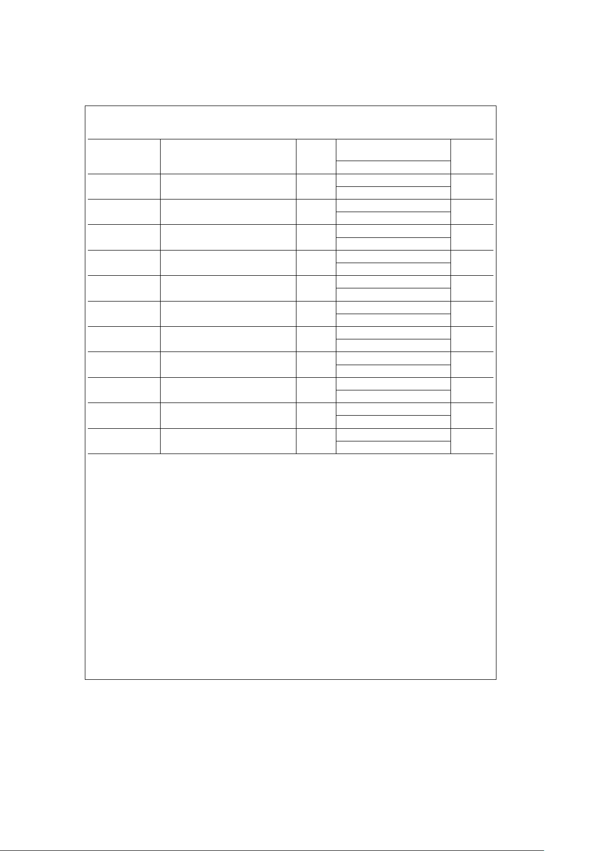
Timing Specifications and Diagrams
TL/F/12147– 10
FIGURE 1. Attribute Memory Read Timing
http://www.national.com23

Timing Specifications and Diagrams (Continued)
Attribute Memory Read Timing Specifications (See
Figure 1
)
Symbol Path
V
CC
(V)
Commercial
Units
T
A
e
0§Ctoa70§C
Min Max
tcR** Read Cycle Time 4.75 300
ns
3.0 300
ta(A)** Address Access Time 4.75 300
ns
3.0 300
ta(CE)** CE1 Access Time 4.75 300
ns
3.0 300
ta(OE) Output Enable Access Time 4.75 150
ns
3.0 150
tdis(OE) Output Disable Time from HOE 4.75 100
ns
3.0 100
tdis(CE) Output Disable Time from CE1 4.75 100
ns
3.0 100
ten(OE)** Output Enable Time from HOE 4.75 5
ns
3.0 5
ten(CE)** Output Enable Time from CE1 4.75 5
ns
3.0 5
tsu(A) Address Setup Time to HOE Falling 4.75 30
ns
3.0 30
th(A)** Address Hold Time from HOE Rising 4.75 20
ns
3.0 20
tsu(CE)** CE1 Setup Time to HOE Falling 4.75 0
ns
3.0 0
th(CE)** CE1 Hold Time from HOE Rising 4.75 20
ns
3.0 20
tv(WT-OE) HWAIT Valid from HOE Falling 4.75 35
ns
3.0 35
tw(WT)** HWAIT Pulse Width 4.75 12000
ns
3.0 12000
tw(OE) HOE Pulse Width 4.75 60
ns
3.0 70
**Parameter guaranteed by design.
http://www.national.com 24

Timing Specifications and Diagrams (Continued)
TL/F/12147– 11
FIGURE 2. Attribute Memory Write Cycle
Attribute Memory Write Cycle Specifications (See
Figure 2
)
Symbol Path
V
CC
(V)
Commercial
Units
T
A
e
0§Ctoa70§C
Min Max
tcW** Write Cycle Time 4.75 250
ns
3.0 250
tw(WE) Write Enable Pulse Width 4.75 60
ns
3.0 60
tsu(A) HADDR Setup Time to HWE Falling 4.75 30
ns
3.0 30
tsu(D-WEH) HDATA Setup Time to HWE Rising 4.75 10
ns
3.0 10
th(D) HDATA Hold Time from HWE Rising 4.75 15
ns
3.0 15
th(A)** HADDR Hold Time from HWE Rising 4.75 20
ns
3.0 20
tsu(OE-WE)** Output Enable Setup to HWE Falling 4.75 10
ns
3.0 10
th(OE-WE)** Output Enable Hold from HWE Rising 4.75 10
ns
3.0 10
tsu(CE)** CE1 Setup Time to HWE Falling 4.75 0
ns
3.0 0
th(CE)** CE1 Hold Time from HWE Rising 4.75 20
ns
3.0 20
**Parameter guaranteed by design.
http://www.national.com25
Timing Specifications and Diagrams (Continued)
TL/F/12147– 12
FIGURE 3. Common Memory Read Timing
http://www.national.com 26
Timing Specifications and Diagrams (Continued)
Common Memory Read Timing Specifications (See
Figure 3
)
Symbol Path
V
CC
(V)
Commercial
Units
T
A
e
0§Ctoa70§C
Min Max
tcR** Read Cycle Time (Note 1) 4.75 120
ns
3.0 125
ten(CE)** Output Enable from CE Falling 4.75 5
ns
3.0 5
ten(OE)** Output Enable from HOE Falling 4.75 5
ns
3.0 5
tsu(A)** HADDR Setup Time to HOE Falling 4.75 10
ns
3.0 10
th(A)** HADDR Hold Time from HOE Rising 4.75 15
ns
3.0 15
tsu(CE)** CE Setup Time from HOE Falling 4.75 0
ns
3.0 0
th(CE)** CE Hold Time from HOE Rising 4.75 15
ns
3.0 15
tdis(CE) HDATA Disable from CE Rising 4.75 50
ns
3.0 50
tdis(OE) HDATA Disable from HOE Rising 4.75 50
ns
3.0 50
td(LD-HD) HDATA Delay from LDATA 4.75 20
ns
3.0 25
tsu(REG-OE)** REG Setup to HOE Falling 4.75 5
ns
3.0 5
**Parameter guaranteed by design.
Note 1: The above Common Memory Read Timing Specifications apply only to 100 ns common memory devices. The Read Cycle Time (tcR) consist of 100 ns
common memory device access time plus the td(LD-HD) delay through the PCM16C010VJG.
http://www.national.com27

Timing Specifications and Diagrams (Continued)
TL/F/12147– 13
FIGURE 4. Common Memory Write Timing
http://www.national.com 28

Timing Specifications and Diagrams (Continued)
Common Memory Write Timing Specifications (See
Figure 4
)
Symbol Path
V
CC
(V)
Commercial
Units
T
A
e
0§Ctoa70§C
Min Max
tcW** Write Cycle Time (Note 1) 4.75 115
ns
3.0 115
tw(WE)** HWE Pulse Width 4.75 60
ns
3.0 60
tsu(A)** HADDR Setup Time from HWE Falling 4.75 10
ns
3.0 10
tsu(D-WEH)** HDATA Setup Time from HWE Rising 4.75 40
ns
3.0 40
th(D)** HDATA Hold Time from HWE Rising 4.75 15
ns
3.0 15
trec(WE)** Write Recovery Time 4.75 15
ns
3.0 15
tsu(OE-WE)** HOE Setup from HWE Falling 4.75 10
ns
3.0 10
th(OE-WE)** HOE Hold from HWE Rising 4.75 10
ns
3.0 10
tsu(CE)** CE Setup Time from HWE Falling 4.75 0
ns
3.0 0
th(CE)** CE Hold Time from HWE Rising 4.75 15
ns
3.0 15
td(MWE) MEMWEH, MEMWEL Delay from HWE 4.75 20
ns
3.0 20
td(LD-HD) LDATA Delay from HDATA 4.75 15
ns
3.0 15
**Parameter guaranteed by design.
Note 1: The above Common Memory Write Timing Specifications apply only to 100 ns SRAM common memory devices. Common memory devices such as
OTPROM, EPROM and Flash do not have standard programming specifications. The Write Cycle Time (tcW) consist of 100 ns SRAM common memory device
access time plus the td(LD-HD) delay through the PCM16C010VJG.
http://www.national.com29

Timing Specifications and Diagrams (Continued)
TL/F/12147– 14
FIGURE 5. I/O Read Timing Specification
http://www.national.com 30

Timing Specifications and Diagrams (Continued)
I/O Read Timing Specifications (See
Figure 5
)
Symbol Path
V
CC
(V)
Commercial
Units
T
A
e
0§Ctoa70§C
Min Max
tsu REG(IORD)** REG Setup to HIORD Falling 4.75 5
ns
3.0 5
tsu CE(IORD)** CE Setup to HIORD Falling 4.75 5
ns
3.0 5
tsu A(IORD)** HADDR Setup to HIORD Falling 4.75 70
ns
3.0 70
tw (IORD) HIORD Pulse Width 4.75 165
ns
3.0 165
tdf INPACK(IORD) INPACK Delay from HIORD Falling 4.75 45
ns
3.0 45
tw(WT)** HWAIT Pulse Width 4.75 12000
ns
3.0 12000
th A(IORD)** HADDR Hold from HIORD Rising 4.75 20
ns
3.0 20
th REG(IORD)** REG Hold from HIORD Rising 4.75 0
ns
3.0 0
th CE(IORD)** CE Hold from HIORD Rising 4.75 20
ns
3.0 20
tdr INPACK(IORD) INPACK Delay from HIORD Rising 4.75 45
ns
3.0 45
th(IORD)** LDATA Hold from HIORD Rising 4.75 0
ns
3.0 0
td(CS) CS Delay from CE Falling 4.75 20
ns
3.0 30
td(CIORD) CIORD Delay from HIORD 4.75 25
ns
3.0 35
td(HDATA) HDATA Delay from LDATA 4.75 20
ns
3.0 25
td BHE(ADR) BHE Delay from HADDR 4.75 20
ns
3.0 25
td(IOIS16) IOIS16 Delay from IOCS16 Falling 4.75 12
ns
3.0 18
td(HWAIT) HWAIT Delay from CWAIT 4.75 25
ns
3.0 30
**Parameter guaranteed by design.
http://www.national.com31
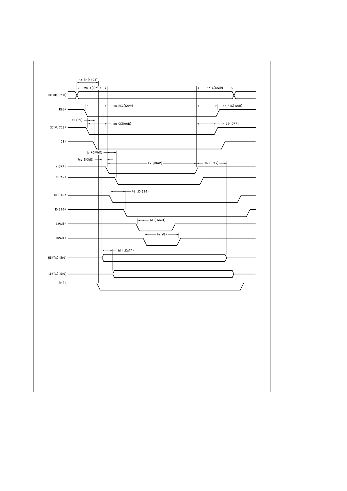
Timing Specifications and Diagrams (Continued)
TL/F/12147– 15
FIGURE 6. I/O Write Timing Specification
http://www.national.com 32

Timing Specifications and Diagrams (Continued)
I/O Write Timing Specifications (See
Figure 6
)
Symbol Path
V
CC
(V)
Commercial
Units
T
A
e
0§Ctoa70§C
Min Max
tsu REG(IOWR) REG Setup to HIOWR Falling 4.75 5
ns
3.0 5
tsu CE(IOWR)** CE Setup to HIOWR Falling 4.75 5
ns
3.0 5
tsu A(IOWR) HADDR Setup to HIOWR Falling 4.75 70
ns
3.0 70
tsu(IOWR) HDATA Setup to HIOWR Falling 4.75 60
ns
3.0 60
tw(IOWR) HIOWR Pulse Width 4.75 165
ns
3.0 165
tw(WT)** HWAIT Pulse Width 4.75 12000
ns
3.0 12000
th A(IOWR)** HADDR Hold from HIOWR Rising 4.75 20
ns
3.0 20
th REG(IOWR)** REG Hold from HIOWR Rising 4.75 0
ns
3.0 0
th CE(IOWR)** CE Hold from HIOWR Rising 4.75 20
ns
3.0 20
th(IOWR)** HDATA Hold from HIOWR Rising 4.75 30
ns
3.0 30
td(CS) CS Delay from CE Falling 4.75 20
ns
3.0 25
td(CIOWR) CIOWR Delay from HIOWR Falling 4.75 25
ns
3.0 30
td(LDATA) LDATA Delay from HDATA 4.75 15
ns
3.0 15
td BHE(ADR) BHE Delay from HADDR 4.75 20
ns
3.0 25
td(IOIS16) IOIS16 Delay from IOCS16 Falling 4.75 13
ns
3.0 13
td(HWAIT) HWAIT Delay from CWAIT 4.75 25
ns
3.0 30
**Parameter guaranteed by design.
http://www.national.com33

Timing Specifications and Diagrams (Continued)
TL/F/12147– 16
Note 1: For HADDR(12:0), REGÝ, CE1Ýand CE2Ýtiming specifications to HOEÝor HIORDÝrefer to the Common Memory Read or I/O Read Timing
Specifications.
*Note 2: The NAND Flash Read Timing Specifications are based upon National’s NM29N16, 16 MBit (2M x 8-Bit) CMOS NAND Flash EEPROM. The NAND Flash
Read Timing Specifications are dependent on the NAND Flash Device.
FIGURE 7. NAND Flash (NM29N16) Read Timing Specification
NAND Flash (NM29N16) Read Timing Specification (See
Figure 7
)
Symbol Path
V
CC
(V)
Commercial
Units
T
A
e
0§Ctoa70§C
Min Max
tw(IORD) HIORD Pulse Width 4.75 165
ns
3.0 165
taHIORD(HDATA) HDATA Access from HIORD Falling 4.75 100*
ns
3.0 100*
th(IORD)** LDATA Hold from HIORD Rising 4.75 0
ns
3.0 0
td(HDATA) HDATA Delay from LDATA 4.75 20
ns
3.0 25
ta(OE)** HDATA Access from HOE Falling 4.75 100*
ns
3.0 100*
td RE(IORD) RE Delay from HIORD 4.75 18
ns
3.0 25
td RE(HOE) RE Delay from HOE 4.75 12
ns
3.0 16
td LDATA(RE) LDATA Delay from RE 4.75 45*
ns
3.0
*Based on Read Access Time of National’s NM29N16.
**Parameter guaranteed by design.
http://www.national.com 34

Timing Specifications and Diagrams (Continued)
TL/F/12147– 17
Note 1: For HADDR(12:0), REGÝ, CE1Ýand CE2Ýtiming specifications to HWEÝor HIOWRÝrefer to the Common Memory Write or I/O Write Timing
Specifications.
Note 2: The NAND Flash Write Timing Specifications are based upon National’s NM29N16, 16 MBit (2M x 8-Bit) CMOS NAND Flash EEPROM. The NAND Flash
Write Timing Specifications are dependent on the NAND Flash Device.
FIGURE 8. NAND Flash (NM29N16) Write Timing Specification
http://www.national.com35

Timing Specifications and Diagrams (Continued)
NAND Flash (NM29N16) Write Timing Specification (See
Figure 8
)
Symbol Path
V
CC
(V)
Commercial
Units
T
A
e
0§Ctoa70§C
Min Max
tsu HDATA(IOWR) HDATA Setup Time to HIOWR Falling 4.75 60
ns
3.0 60
tsu HDATA(HWE)** HDATA Setup Time to HWE Rising 4.75 40
ns
3.0 40
th(IOWR)** HDATA Hold from HIOWR Rising 4.75 30
ns
3.0 30
th HDATA(HWE)** HDATA Hold Time from HWE Rising 4.75 30
ns
3.0 30
td WE(IOWR) WE Delay from HIOWR 4.75 18
ns
3.0 25
td WE(HWE) WE Delay from HWE 4.75 12
ns
3.0 16
td CEÐNAND(3:0)
Ý
CEÐNAND(3:0)ÝDelay from HIOWR 4.75 27
ns
(IOWR)
3.0 32
td ALE/CLE(IOWR) ALE/CLE Delay from HIOWR 4.75 22
ns
3.0 27
tw (IOWR) HIOWR Pulse Width 4.75 165
ns
3.0 165
tw (HWE)** HWE Pulse Width 4.75 60
ns
3.0 60
td(LDATA) LDATA Delay from HDATA 4.75 15
ns
3.0 15
**Parameter guaranteed by design
http://www.national.com 36

Timing Specifications and Diagrams (Continued)
PCM16C010 IC Specific Timing Specifications
Symbol Path
V
CC
(V)
Commercial
Units
T
A
e
0§Ctoa70§C
Min Max
td(CS) CS from Valid Address 4.75 30
ns
3.0 40
td(IREQ) IREQ Delay from CINT 4.75 20
ns
3.0 25
td(SPKR) SPKR Delay from SPKÐIN 4.75 17
ns
3.0 20
td(SRESET) SRESET Delay from RESET 4.75 30
ns
3.0 35
td(PCNTL) PCNTL Delay from HWE 4.75 35
ns
3.0 40
td(FCLK) FCLK Delay from MCLK 4.75 25
ns
3.0 30
Frequency MCLK 4.75 5 30
MHz
3.0 5 30
**Parameter guaranteed by design.
Capacitance
Symbol Parameter Typical Units Conditions
C
IN
Input Pin Capacitance 3 pF V
CC
e
OPEN
C
OUT
Output Pin Capacitance 5 pF V
CC
e
5.0V
C
I/O
Input/Output Capacitance 5 pF V
CC
e
5.0V
C
PD
Power Dissipation Capacitance 42 pF V
CC
e
5.0V
Typical Applications
Dual Function Card with NAND (NM29N16) Flash and Modem.
References
1. PC Card Standard
2. National Semiconductor 1992 Memory Databook. Application Note AN758.
3. National NM29N16, 16-MBit (2M x 8-bit) CMOS NAND
Flash E
2
PROM Datasheet.
4. PCM16C00 Datasheet.
http://www.national.com37

PCM16C010 Configurable PC Card Interface Chip
Physical Dimensions millimeters
100-Pin TQFP
100-Lead (14 mm x 14 mm) Molded Thin Plastic Quad Flatpak (JEDEC)
NS Package Number VJG100A
LIFE SUPPORT POLICY
NATIONAL’S PRODUCTS ARE NOT AUTHORIZED FOR USE AS CRITICAL COMPONENTS IN LIFE SUPPORT
DEVICES OR SYSTEMS WITHOUT THE EXPRESS WRITTEN APPROVAL OF THE PRESIDENT OF NATIONAL
SEMICONDUCTOR CORPORATION. As used herein:
1. Life support devices or systems are devices or 2. A critical component is any component of a life
systems which, (a) are intended for surgical implant support device or system whose failure to perform can
into the body, or (b) support or sustain life, and whose be reasonably expected to cause the failure of the life
failure to perform, when properly used in accordance support device or system, or to affect its safety or
with instructions for use provided in the labeling, can effectiveness.
be reasonably expected to result in a significant injury
to the user.
National Semiconductor National Semiconductor National Semiconductor National Semiconductor
Corporation Europe Southeast Asia Japan Ltd.
Fax:
a
49 (0) 180-530 85 86 Fax: (852) 2376 3901 Tel: 81-3-5620-7561
Americas
Email: europe.support
@
nsc.com Email: sea.support@nsc.com Fax: 81-3-5620-6179
Tel: 1(800) 272-9959
Deutsch Tel:
a
49 (0) 180-530 85 85
Fax: 1(800) 737-7018
English Tel:
a
49 (0) 180-532 78 32
Email: support
@
nsc.com
Fran3ais Tel:
a
49 (0) 180-532 93 58
Italiano Tel:
a
49 (0) 180-534 16 80
http://www.national.com
National does not assume any responsibility for use of any circuitry described, no circuit patent licenses are implied and National reserves the right at any time without notice to change said circuitry and specifications.
 Loading...