NSC PC87332VLJ Datasheet
PC87332VLJ (3.3V/5V) and PC87332VLJ-5 (5V)
(SuperI/O
TM
III Premium Green)
Floppy Disk Controller, Dual UARTs, IEEE1284
Parallel Port, and IDE Interface
PRELIMINARY
May 1995
PC87332VLJ (3.3V/5V) and PC87332VLJ-5 (5V) (SuperI/O
Floppy Disk Controller, Dual UARTs, IEEE1284 Parallel Port, and IDE Interface
General Description
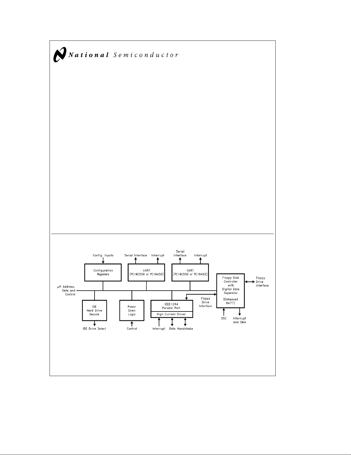
The PC87332VLJ and PC87332VLJ-5 are single chip solutions for most commonly used I/O peripherals in ISA, EISA
and MicroChannel
Floppy Disk Controller (FDC), two full featured UARTs, an
IEEE 1284 compatible parallel port and all the necessary
control logic for an IDE interface. Standard PC-AT
decoding for all the peripherals and a set of configuration
registers are also implemented in this highly integrated
member of the SuperI/O family. Advanced power management features and mixed voltage operation in the VLJ version make the PC87332 chips an ideal for low-power and/or
portable personal computer applications.
The PC87332 FDC uses a high performance digital data
separator eliminating the need for any external filter components. It is fully compatible with the PC8477 and incorporates a superset of DP8473, NEC mPD765 and N82077 floppy disk controller functions. All popular 5.25
py drives, including the 2.88 MB 3.5
ported. In addition, automatic media sense and 2 Mbps tape
drive support are provided by the FDC.
The two UARTs are fully NS16450 and NS16550 compatible. Both ports support MIDI baud rates. (Continued)
based computers. It incorporates a
É
É
and 3.5×flop-
×
floppy drive, are sup-
×
address
Block Diagram
Features
Y
Floppy Disk Controller:
Ð Software compatible with the DP8473, the 765A and
the N82077
Ð 16-byte FIFO (disabled by default)
Ð Burst and Non-Burst modes
Ð Perpendicular Recording drive support
Ð New high-performance internal digital data separator
(no external filter components required)
Ð Low-power CMOS with enhanced power-down mode
Ð Automatic media-sense support
Ð Supports fast 2 Mbps and standard 1 Mbps/
500 kbps/250 kbps tape drives
Y
Bidirectional Parallel Port:
Ð Enhanced Parallel Port (EPP) compatible
Ð Extended Capabilities Port (ECP) compatible, includ-
ing level 2 support
Ð Bidirectional under either software or hardware
control
Ð Ability to multiplex FDC signals on parallel port pins
allows use of an external Floppy Disk Drive (FDD)
Ð Includes protection circuit to prevent damage to the
parallel port when a connected printer is powered up
or is operated at a higher voltage (Continued)
TM
III Premium Green)
TL/C/11930– 1
TRI-STATEÉis a registered trademark of National Semiconductor Corporation.
TM
SuperI/O
is a trademark of National Semiconductor Corporation.
IBM
, MicroChannelÉ, PC-ATÉand PS/2Éare registered trademarks of International Business Machines Corporation.
É
C
1995 National Semiconductor Corporation RRD-B30M65/Printed in U. S. A.
TL/C/11930

General Description (Continued)
The parallel port is fully IEEE 1284 level 2 compatible. The
SPP (Standard Parallel Port) is fully compatible with ISA,
EISA and MicroChannel parallel ports. In addition to the
SPP, EPP (Enhanced Parallel Port) and ECP (Extended Capabilities Port) modes are supported by the parallel port.
All IDE control signals are provided by the PC87332. Only
external signal buffers are required to implement a complete
IDE interface.
A set of eight configuration registers are provided to control
various functions of the PC87332. These registers are accessed using two 8-bit wide index and data registers. The
ISA I/O address of the register pair can be relocated using a
power-up strapping option.
When idle, advanced power management features allows
the PC87332 to enter extremely low power modes under
hardware or software control. The PC87332VLJ can operate from a 5V or a 3.3V power supply. An unique I/O cell
structure allows the PC87332VLJ to interface directly with
5V external components while operating from a 3.3V power
supply.
Features (Continued)
Y
UARTs:
Ð Software compatible with the PC16550A and
PC16450
Ð MIDI baud rate support
Y
IDE Control Logic:
Ð All IDE control signals. Only external signal buffers
required to implement full IDE interface
Y
Address Decoder:
Ð Provides selection of all primary and secondary ISA
addresses including COM1– 4 and LPTA –C
Y
Enhanced Power Management:
Ð Special configuration registers for power-down
Ð Enhanced programmable power-down FDC
command
Ð Auto power-down and wake-up modes
Ð 3 special pins for power management
Ð Typical current consumption during power-down is
less than 10 mA
Ð Reduced pin leakage current
Y
Mixed Voltage Support:
Ð Supports standard 5V operation
Ð Supports 3.3V operation
Ð Supports mixed internal 3.3V operation with 3.3V/5V
external configuration
Y
General:
Ð 100% compatible with ISA, EISA, and MicroChannel
architectures
Ð 100-Pin PQFP package is pin compatible with the
PC87312 and PC87322VF
2

1.0 PIN DESCRIPTION
2.0 CONFIGURATION REGISTERS
2.1 Overview
2.2 Software Configuration
2.3 Hardware Configuration
2.4 Index and Data Registers
2.5 Base Configuration Registers
2.5.1 Function Enable Register (FER)
2.5.2 Function Address Register (FAR)
2.5.3 Power and Test Register (PTR)
2.5.4 Function Control Register (FCR)
2.5.5 Printer Control Register (PCR)
2.5.6 Power Management Control Register (PMC)
2.5.7 Tape, UARTs and Parallel Port
Configuration Register (TUP)
2.5.8 SIO Identification Register (SID)
2.6 Power-Down Options
2.6.1 Recommended Power-Down
MethodsÐGroup 1
2.6.2 Recommended Power-Down
MethodsÐGroup 2
2.7 Power-Up Procedure and Considerations
2.7.1 Crystal Stabilization
2.7.2 UART Power-Up
2.7.3 FDC Power-Up
3.0 FDC REGISTER DESCRIPTION
3.1 FDC Control Registers
3.1.1 Status Registger A (SRA) Read Only
3.1.2 Status Register B (SRB) Read Only
3.1.3 Digital Output Register (DOR) Read/Write
3.1.4 Tape Drive Register (TDR) Read/Write
3.1.5 Main Status Register (MSR) Read Only
3.1.6 Data Rate Select Register (DSR) Write Only
3.1.7 Data Register (FIFO) Read/Write
3.1.8 Digital Input Register (DIR) Read Only
3.1.9 Configuration Control Register (CCR) Write Only
3.2 Result Phase Status Registers
3.2.1 Status Register 0 (ST0)
3.2.2 Status Register 1 (ST1)
3.2.3 Status Register 2 (ST2)
3.2.4 Status Register 3 (ST3)
Table of Contents
4.0 FDC COMMAND SET DESCRIPTION
4.1 Command Description
4.1.1 Configure Command
4.1.2 Dumpreg Command
4.1.3 Format Track Command
4.1.4 Invalid Command
4.1.5 Lock Command
4.1.6 Mode Command
4.1.7 NSC Command
4.1.8 Perpendicular Mode Command
4.1.9 Read Data Command
4.1.10 Read Deleted Data Command
4.1.11 Read ID Command
4.1.12 Read A Track Command
4.1.13 Recalibrate Command
4.1.14 Relative Seek Command
4.1.15 Scan Commands
4.1.16 Seek Command
4.1.17 Sense Drive Status Command
4.1.18 Sense Interrupt Command
4.1.19 Set Track Command
4.1.20 Specify Command
4.1.21 Verify Command
4.1.22 Version Command
4.1.23 Write Data Command
4.1.24 Write Deleted Data
4.2 Command Set Summary
4.3 Mnemonic Definitons for FDC Commands
5.0 FDC FUNCTIONAL DESCRIPTION
5.1 Microprocessor Interface
5.2 Modes of Operation
5.3 Controller Phases
5.3.1 Command Phase
5.3.2 Execution Phase
5.3.2.1 DMA ModeÐFIFO Disabled
5.3.2.2 DMA ModeÐFIFO Enabled
5.3.2.3 Interrupt ModeÐFIFO Disabled
5.3.2.4 Interrupt ModeÐFIFO Enabled
5.3.2.5 Software Polling
5.3.3 Result Phase
5.3.4 Idle Phase
5.3.5 Drive Polling Phase
5.4 Data Separator
5.5 Crystal Oscillator
5.6 Perpendicular Recording Mode
5.7 Data Rate Selection
5.8 Write Precompensation
5.9 FDC Low Power Mode Logic
5.10 Reset Operation
3

Table of Contents (Continued)
6.0 SERIAL PORTS
6.1 Serial Port Registers
6.2 Line Control Register (LCR)
6.3 Programmable Baud Rate Generator
6.4 Line Status Register (LSR)
6.5 FIFO Control Register
6.6 Interrupt Identification Register (IIR)
6.7 Interrupt Enable Register (IER)
6.8 MODEM Control Register (MCR)
6.9 MODEM Status Register (MSR)
6.10 Scratchpad Register (SCR)
7.0 PARALLEL PORT
7.1 Introduction
7.2 Data Register (DTR)
7.3 Status Register (STR)
7.4 Control Register (CTR)
7.5 Enhanced Parallel Port Operation
7.6 Extended Capabilities Parallel Port (ECP)
7.6.1 Introduction
7.6.2 Software Operation
7.7 Register Definitions
7.8 Software Controlled Data Transfer
7.9 Automatic Data Transfer (Modes 010 and 011)
7.10 FIFO Test Access (Mode 110)
7.11 Configuration Registers Access (Mode 111)
7.12 Interrupt Generation
(Modes 000 and 001)
7.9.1 Forward Direction (Bit 5 of DCR
7.9.2 ECP (Forward) Write Cycle
7.9.3 Backward Direction (bit 5 of DCR is 1)
7.9.4 ECP (Backward) Read Cycle
e
8.0 INTEGRATED DEVICE ELECTRONICS
INTERFACE (IDE)
8.1 Introduction
8.2 IDE Signals
9.0 ELECTRICAL CHARACTERISTICS
9.1 DC Electrical Characteristics
9.2 DC Electrical Characteristics
9.3 AC Electrical Characteristics
9.3.1 AC Test Conditions
9.3.2 Clock Timing
9.3.3 Microprocessor Interface Timing
9.3.4 Baud Out Timing
9.3.5 Transmitter Timing
9.3.6 Receiver Timing
9.3.7 MODEM Control Timing
9.3.8 DMA Timing
9.3.9 Reset Timing
9.3.10 Write Data Timing
9.3.11 Drive Control Timing
9.3.12 Read Data Timing
9.3.13 IDE Timing
9.3.14 Parallel Port Timing
9.3.15 Enhanced Parallel Port Timing
9.3.16 Extended Capabilities Port Timing
0)
4

List of Figures
FIGURE 2-1 PC87332VLJ/PC87332VLJ-5 Configuration Registers
FIGURE 2-2 PC87332 Four Floppy Drive Circuit Example
FIGURE 3-1 FDC Functional Block Diagram
FIGURE 4-1 FDC Command Structure
FIGURE 4-2 IBM, Perpendicular, and ISO Formats Supported by the Format Command
FIGURE 5-1 PC87332 Dynamic Window Margin Performance
FIGURE 5-2 Read Data AlgorithmÐState Diagram
FIGURE 5-3 Perpendicular Recording Drive R/W Head and Pre-Erase Head
FIGURE 6-1 PC87332 Composite Serial Data
FIGURE 6-2 Reciever FIFO Trigger Level
FIGURE 7-1 EPP 1.7 Address Write
FIGURE 7-2 EPP 1.7 Address Read
FIGURE 7-3 EPP Write with ZWS
FIGURE 7-4 EPP 1.9 Address Write
FIGURE 7-5 EPP 1.9 Address Read
FIGURE 7-6 ECP (Forward) Write Cycle
FIGURE 7-7 ECP (Backward) Read Cycle
FIGURE 8-1 IDE Interface Signal Equations (Non-DMA)
FIGURE 9-1 Clock Timing
FIGURE 9-2 Microprocessor Read Timing
FIGURE 9-3 Microprocessor Write Timing
FIGURE 9-4 Baud Out Timing
FIGURE 9-5 Transmitter Timing
FIGURE 9-6a Sample Clock Timing
FIGURE 9-6b Receiver Timing
FIGURE 9-6c Mode Receiver Timing
FIGURE 9-6d Timeout Receiver Timing
FIGURE 9-7 MODEM Control Timing
FIGURE 9-8 DMA Timing
FIGURE 9-9 Reset Timing
FIGURE 9-10 Write Data Timing
FIGURE 9-11 Drive Control Timing
FIGURE 9-12 Read Data Timing
FIGURE 9-13 IDE Timing
FIGURE 9-14 Compatible Mode Parallel Port Interrupt Timing
FIGURE 9-15 Extended Mode Parallel Port Interrupt Timing
FIGURE 9-16 Typical Parallel Port Data Exchange
FIGURE 9-17 Enhanced Parallel Port Timing
FIGURE 9-18 ECP Parallel Port Forward Timing Diagram
FIGURE 9-19 ECP Parallel Port Backward Timing Diagram
5

List of Tables
TABLE 1-1 Pin Descriptions (Alphabetical)
TABLE 2-1 Default Configurations Controlled by Hardware
TABLE 2-2 Index and Data Register Optional Locations
TABLE 2-3 Encoded Drive and Motor Pin Information
TABLE 2-4 Primary and Secondary Drive Address Selection
TABLE 2-5 Parallel Port Addresses
TABLE 2-6 COM Port Selection for UART1
TABLE 2-7 COM Port Selection for UART2
TABLE 2-8 Address Selection for COM3 and COM4
TABLE 2-9 Logical Drive Exchange
TABLE 2-10 Parallel Port Mode
TABLE 2-11 Methods to Achieve Group 1 Power-Down Modes
TABLE 3-1 Register Description and Addresses
TABLE 3-2 Drive Enable Values
TABLE 3-3 Media ID Bit Functions
TABLE 3-4 Tape Drive Assignment Values
TABLE 3-5 Write Precompensation Delays
TABLE 3-6 Default Precompensation Delays
TABLE 3-7 Data Rate Select Encoding
TABLE 4-1 Typical Format Gap Length Values
TABLE 4-2 Typical Format GAP3 Length Values Based on PC Compatible Diskette Media
TABLE 4-3 DENSEL Default Encoding
TABLE 4-4 DENSEL Encoding
TABLE 4-5 Head Settle Time Calculation
TABLE 4-6 Effect of Drive Mode and Data Rate on Format and Write Commands
TABLE 4-7 Effect of GAP and WG on Format and Write Commands
TABLE 4-8 Sector Size Selection
TABLE 4-9 SK Effect on the Read Data Command
TABLE 4-10 Result Phase Termination Values with No Error
TABLE 4-11 SK Effect on the Read Deleted Data Command
TABLE 4-12 Maximum Recalibrate Step Pulses Based on R255 and ETR
TABLE 4-13 Scan Command Termination Values
TABLE 4-14 Status Register 0 Termination Codes
TABLE 4-15 Set Track Register Address
TABLE 4-16 Step Rate Time (SRT) Values
TABLE 4-17 Motor Off Time (MFT) Values
TABLE 4-18 Motor On Time (MNT) Values
TABLE 4-19 Verify Command Result Phase
TABLE 6-1 PC87332 UART Register Addresses (AEN
TABLE 6-2 PC87332 Register Summary for an Individual UART Channel
TABLE 6-3 PC87332 UART Reset Configuration
TABLE 6-4 PC87332 UART Divisors, Baud Rates and Clock Frequencies
TABLE 6-5 PC87332 Interrupt Control Functions
TABLE 7-1 Parallel Interface Register Addresses
TABLE 7-2 Standard Parallel Port Modes Selection
TABLE 7-3 SPP Data Register Read and Write Modes
TABLE 7-4 Parallel Port Reset States
TABLE 7-5 EPP Registers
TABLE 7-6 Parallel Port Pin Out
TABLE 7-7 ECP Registers Summary
TABLE 8-1 IDE Registers and Their ISA Addresses
WDW
Values
Values
TABLE 9-1 Nominal t
TABLE 9-2 Minimum t
ICP,tDRP
e
0)
6
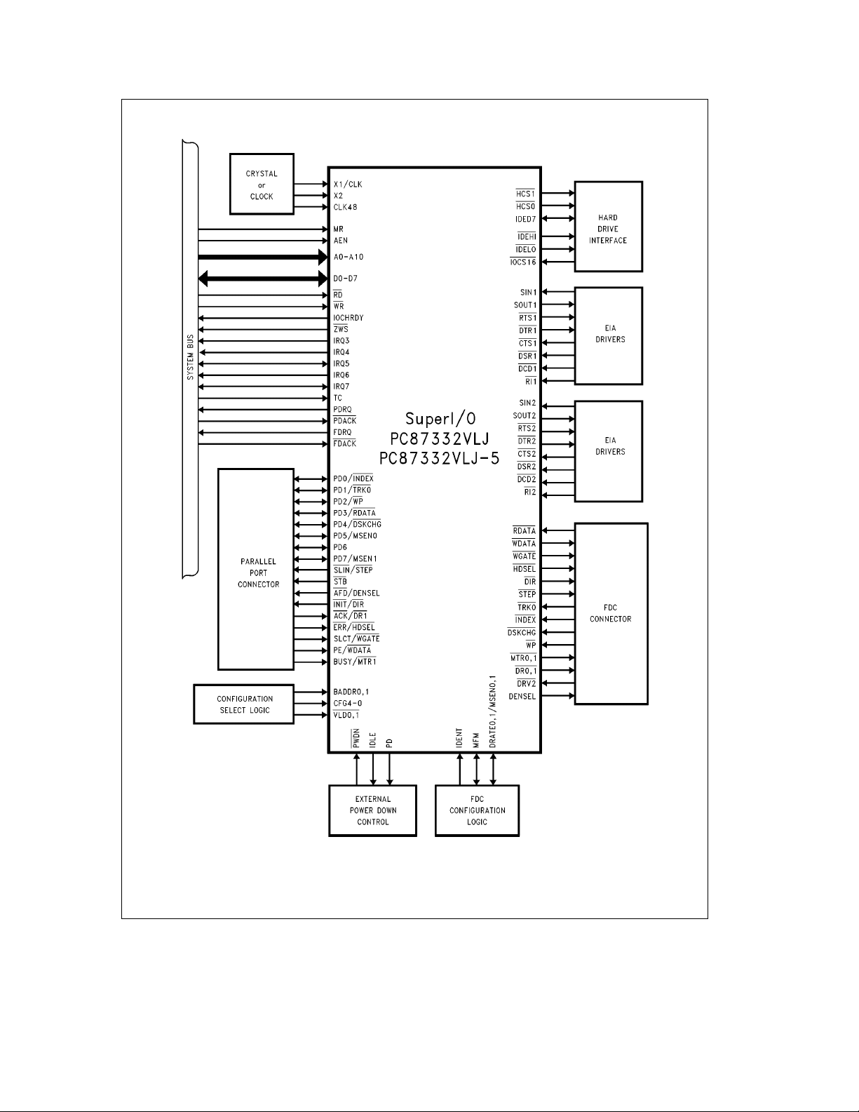
Basic Configuration
TL/C/11930– 2
7
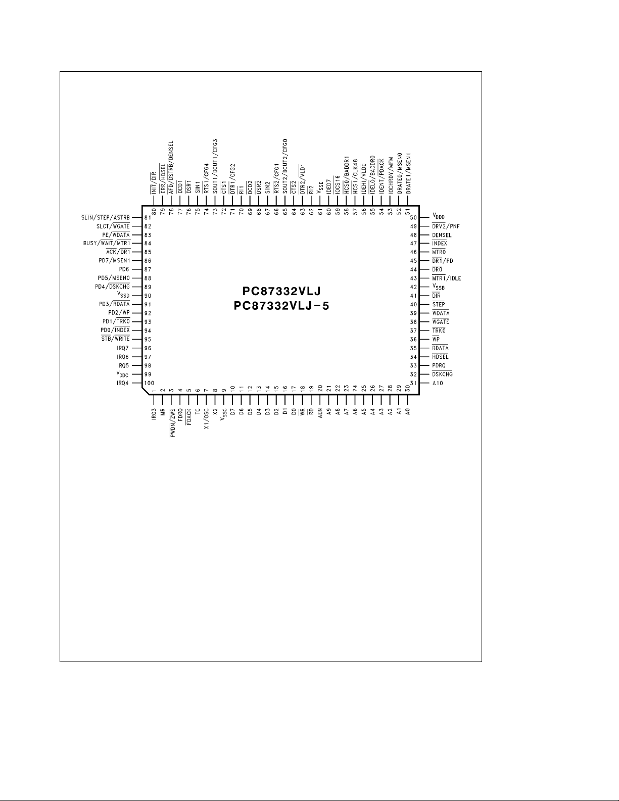
1.0 Pin Description
Connection Diagrams
Plastic Quad Flatpak (PQFP), EIAJ
Order Number PC87332VLJ or PC87332VLJ-5
See NS Package Number VLJ100A
8
TL/C/11930– 3
1.0 Pin Description (Continued)
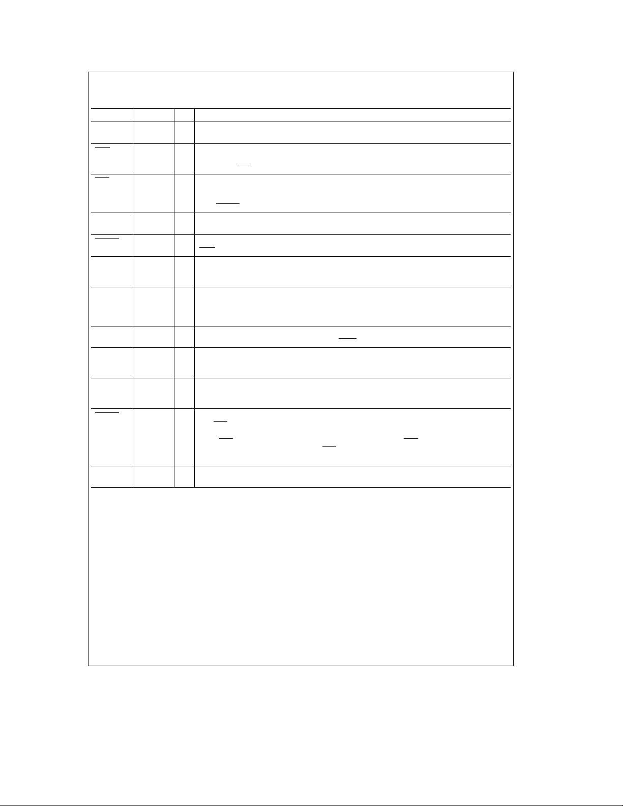
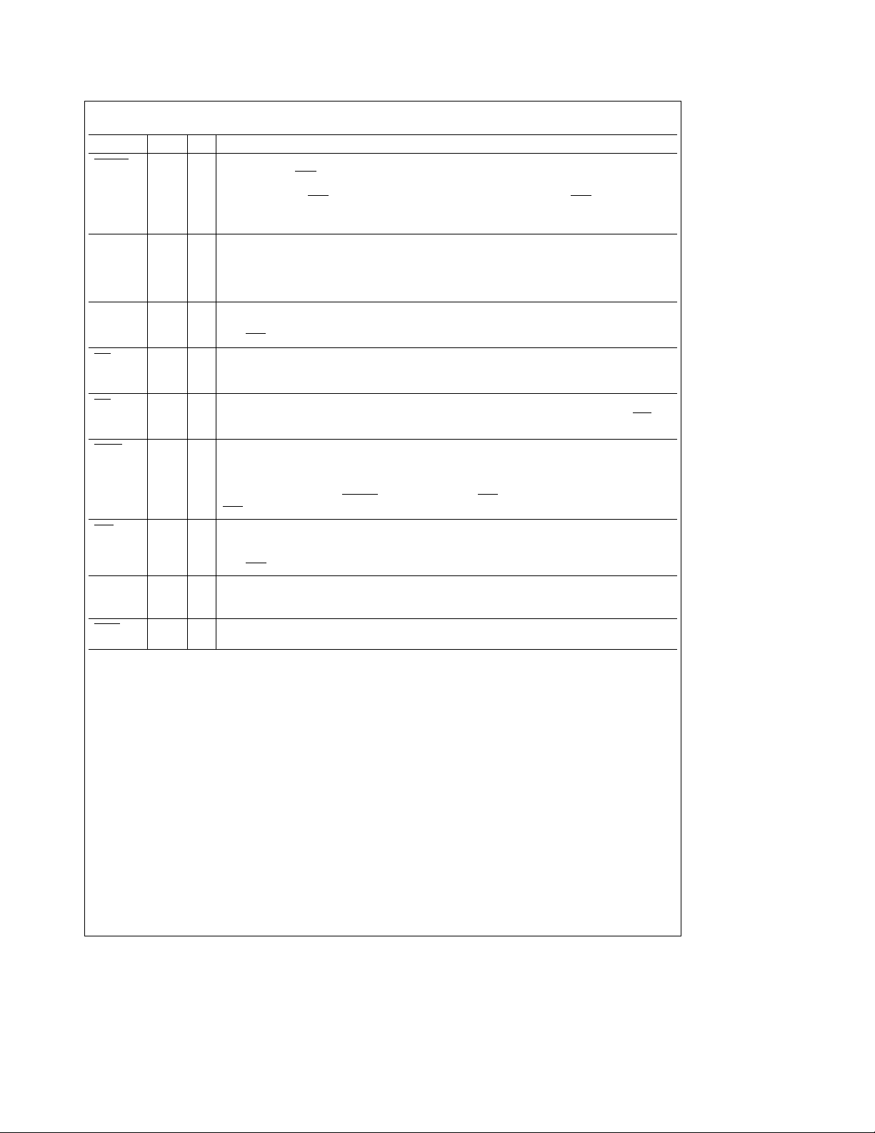
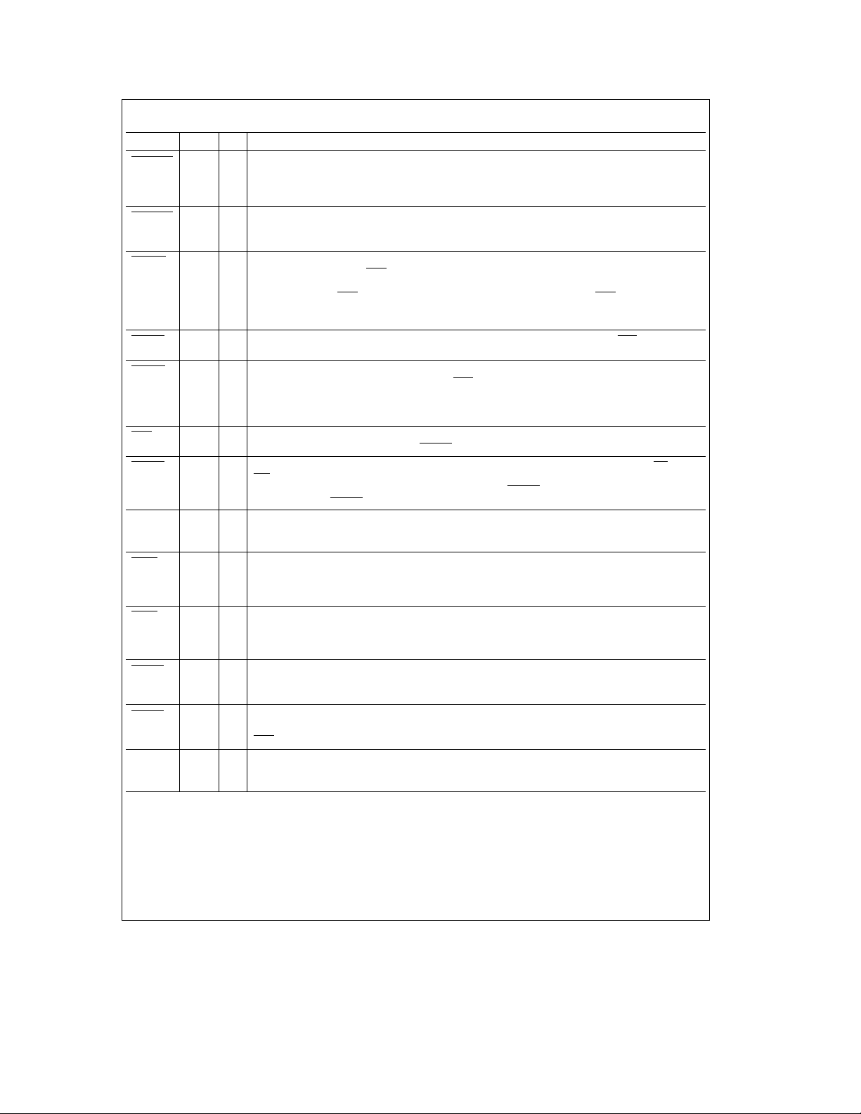
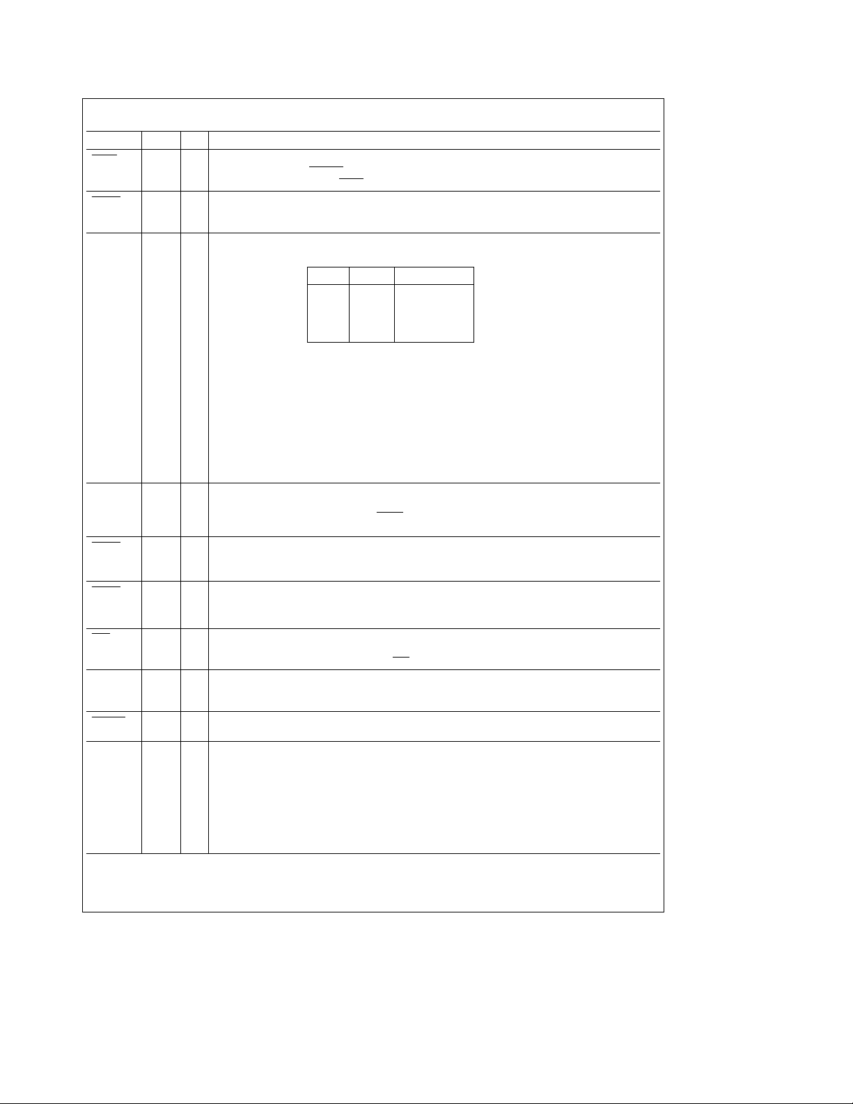
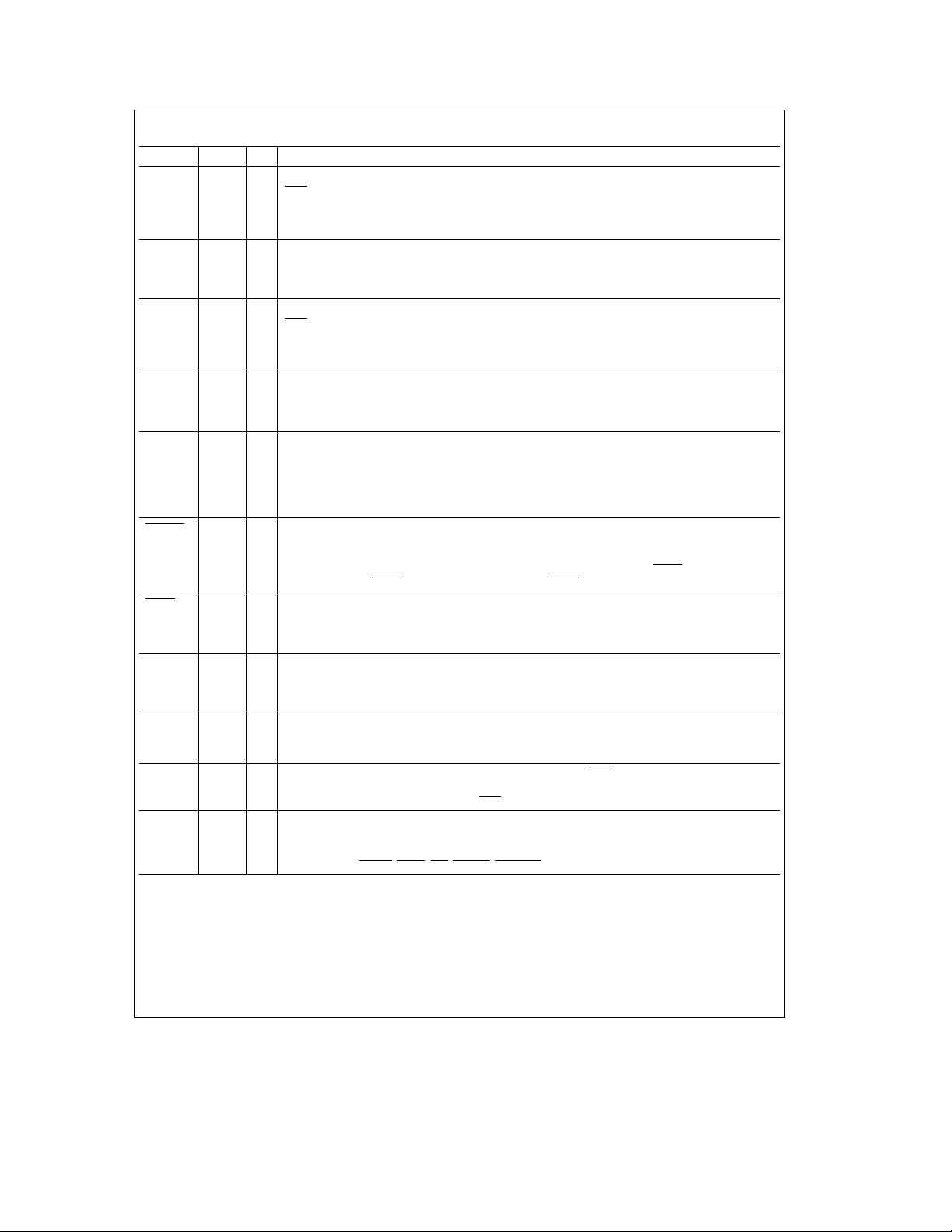
TABLE 1-1. Pin Descriptions (Alphabetical)
Symbol Pin I/O Function
A10–A0 21–31 I Address. These microprocessor address lines determine which internal register is accessed. A0–
ACK 85 I Acknowledge. This input is pulsed low by a connected printer to indicate that it has received data
AFD 78 I/O Automatic Feed XT. When this signal is low the connected printer should automatically line feed
AEN 20 I Address Enable. This input disables function selection via A10 – A0 when it is high. Access during
ASTRB 81 O Address Strobe. This signal is used in EPP mode as an address strobe. It is active low. (See
BADDR0,1 55, 58 I Base Address. These bits determine one of four base addresses from which the Index and Data
BOUT1,2 73, 65 O BAUD Output. This multi-function pin provides the associated serial channel Baud Rate generator
BUSY 84 I Busy. This pin is set high by the printer when it cannot accept another character. It has a nominal
CFG0–4 65, 66, 71 I Configuration on Power-up. These CMOS inputs select 1 of 32 default configurations in which
73, 74
CLK48 57 I Clock 48. This pin is the CLK48 reset strap option. During reset the value of this pin is latched into
CTS1,2 72, 64 I Clear to Send. When low this indicates that the MODEM or data set is ready to exchange data.
D7–D0 10–17 I/O Data. Bi-directional data lines to the microprocessor. D0 is the LSB and D7 is the MSB. These
A10 are don’t cares during a DMA transfer.
from the parallel port. This pin has a nominal 25 kX pull-up resistor attached to it. (This pin is
shared with DR1
after each line is printed. This pin is in a TRI-STATE
corresponding Control Register bit. The system should pull this pin high using a 4.7 kX resistor.
(See DSTRB
DMA transfer is NOT affected by this pin.
SLIN
and Table 7-5 for further information.)
Registers are offset (See Table 2-2). An internal pull-down resistor of 30 kX is present on this pin.
Usea10kXresistor to pull this pin to V
output signal, when test mode is selected in the Power and Test Configuration Register and the
DLAB bit (LCR7) is set. After Master Reset this pin provides the SOUT function. (See SOUT and
CFG0–4 for further information.)
25 kX pull-down resistor attached to it. (See WAIT
the PC87334VLJ/PC87334VJG powers-up (See Table 2-1). An internal pull-down resistor of 30
kX is present on each pin. Use a 10 kX resistor to pull these pins to V
bit 0 of TUP (CLK48 bit). A 30 kX internal pull-down resistor is present on this pin. Use a 10 kX
resistor to pull it high during reset.
The CTS
of the MODEM Status Register (MSR) for the appropriate serial channel. Bit 4 is the complement
of the CTS
since the previous reading of the MSR. CTS
Note: Whenever the DCTS bit of the MSR is set an interrupt is generated if MODEM Status interrupts are enabled.
signals all have 24 mA (sink) buffered outputs.
. See Table 7-5 for further information.)
condition 10 ns aftera0isloaded into the
É
and Table 7-5 for further information.)
.
CC
and Table 7-5 for further information.)
.
CC
signal is a MODEM status input whose condition the CPU can test by reading bit 4 (CTS)
signal. Bit 0 (DCTS) of the MSR indicates whether the CTS input has changed state
has no effect on the transmitter.
9
1.0 Pin Description (Continued)
Symbol Pin I/O Function
DCD1,2 77, 69 I Data Carrier Detect. When low this signal indicates that the MODEM or data set has detected the
DENSEL
Normal 48 O Density Select. Indicates that a high FDC density data rate (500 kbps, 1 Mbps or 2 Mbps) or a low
Mode
DENSEL
PPM 78 O Density Select. This pin provides an additional Density Select signal in PPM Mode when PNF
Mode
DIR
Normal 41 O Direction. This output determines the direction of the floppy disk drive (FDD) head movement (active
Mode
DIR
PPM 80 O Direction. This pin provides an additional direction signal in PPM Mode when PNFe0. (See INIT and
Mode
DR0,1
Normal 44, 45 O Drive SeIect 0,1. These are the decoded Drive Select outputs that are controlled by the Digital Output
Mode
DR1
PPM 85 O Drive Select 1. This pin provides an additional Drive Select signal in PPM Mode when PNFe0. It is
Mode
DRATE0,1 52, 51 O Data Rate 0,1. These outputs reflect the currently selected FDC data rate (bits 0 and 1 in the
DRV2 49 I Drive2. This input indicates whether a second floppy disk drive has been installed. The state of this
data carrier.The DCD
7 (DCD) of the MODEM Status Register (MSR) for the appropriate serial channel. Bit 7 is the
complement of the DCD
changed state since the previous reading of the MSR.
Note: Whenever the DDCD bit of the MSR is set, an interrupt is generated if MODEM Status interrupts are enabled.
density data rate (250 kbps or 300 kbps) is selected. DENSEL is active high for high density (5.25
drives) when IDENT is high, and active low for high density (3.5
is also programmable via the Mode command (see Section 4.2.6).
(See AFD and Table 7-5 for further information.)
e
step in, inactiveestep out) during a seek operation. During reads or writes, DIR is inactive.
Table 7-5 for further information.)
Register bits D0, D1. The Drive Select outputs are gated with DOR bits 4–7. These are active low
outputs. They are encoded with information to control four FDDs when bit 4 of the Function Enable
Register (FER) is set. (See MTR0,1
DR1
when bit 4 of Function Control Register (FCR) is set. (See Table 7-5 for further information.)
drive select 1 when bit 4 of FCR is 0. It is drive select 0 when bit 4 of FCR is 1. This signal is active low.
(See ACK
Configuration Control Register (CCR) or the Data Rate Select Register (DSR), whichever was written
to last). The pins are totem-pole buffered outputs (6 mA sink, 6 mA source).
pin is available from Status Register A in PS/2Émode. (See PNF for further information.)
and Table 7-5 for further information.)
signal is a MODEM status input whose condition the CPU can test by reading bit
signal. Bit 3 (DDCD) of the MSR indicates whether the DCD input has
drives) when IDENT is low. DENSEL
×
e
for more information.) DR0 exchanges logical drive values with
×
0.
10
1.0 Pin Description (Continued)
Symbol Pin I/O Function
DSKCHG
Normal 32 I Disk Change. This input indicates if the drive door has been opened. The state of this pin is available
Mode
DSKCHG
PPM 89 I Disk Change. This pin provides an additional Disk Change signal in PPM Mode when PNFe0. (See
Mode
DSR1,2 76, 68 I Data Set Ready. When low this signal indicates that the data set or MODEM is ready to establish a
DSTRB 78 O Data Strobe. This signal is used in EPP mode as a data strobe. It is active low. (See AFD and Table 7-5
DTR1,2 71, 63 O Data Terminal Ready. When low, this output indicates to the MODEM or data set that the UART is
ERR 79 I Error. A connected printer sets this input low when it has detected an error. This pin has a nominal 25
FDACK 5IDMA Acknowledge. Active low input to acknowledge the FDC DMA request and enable the RD and
FDRQ 4 O DMA Request. Active high output to signal the DMA controller that a FDC data transfer is needed.
HCS0 58 O Hard Drive Chip Select 0. This output is active in the AT mode when 1) the hard drive registers from
HCS1 57 O Hard Drive Chip Select 1. This output is active in the AT mode when 1) the hard drive registers from
HDSEL
Normal 34 O Head Select. This output determines which side of the FDD is accessed. When active, the head
Mode
HDSEL
PPM 79 O Head Select. This pin provides an additional Head Select signal in PPM Mode when PNFe0. (See
Mode
IDED7 60 I/O IDE Bit 7. This pin provides the data bus bit 7 signal to the IDE hard drive during accesses in the
from the Digital Input register. This pin can also be configured as the Read Gate (RGATE) data
separator diagnostic input via the Mode command (see Section 4.2.6).
PD4 and Table 7-5 for further information.)
communications link. The DSR
reading bit 5 (DSR) of the MODEM Status Register (MSR) for the appropriate channel. Bit 5 is the
complement of the DSR
states since the previous reading of the MSR. (See IRRX for further information.)
Note: Whenever the DDSR bit of the MSR is set, an interrupt is generated If MODEM Status interrupts are enabled.
for further information.)
ready to establish a communications link. The DTR
bit 0 (DTR) of the MODEM Control Register to a high level. A Master Reset operation sets this signal to
its inactive (high) state. Loop mode operation holds this signal to its inactive state. (See CFG4–0 for
further information.)
kX pull-up resistor attached to it. (See HDSEL
WR
inputs during a DMA transfer. When in PC-ATÉor Model 30 mode, this signal is enabled by bit D3
of the Digital Output Register (DOR). When in PS/2 mode, FDACK
DOR is reserved. FDACK
When in PC-AT or Model 30 mode, this signal is enabled by bit D3 of the DOR. When in PS/2 mode,
FDRQ is always enabled, and bit D3 of the DOR is reserved.
1F0–1F7h are selected and the primary address is used or 2) the hard drive registers from 170 –177h
are selected and the secondary address is used. This output is inactive if the IDE interface is disabled
via the Configuration Register. (See BADDR1 for further information.)
3F6–7 are selected and the primary address is used or 2) the hard drive registers from 376 –377 are
selected and the secondary address is used. This output is also inactive, if the IDE interface is disabled
via the Configuration Register. (See CLK48 for further information.)
selects side 1. When inactive, the head selects side 0.
ERR and Table 7-5 for further information.)
address range 1F0–1F7h, 170 –177h, 3F6h and 376h. This pin is in TRI-STATE during read or write
accesses to 3F7h and 377h.
signal is a MODEM status input whose condition the CPU can test by
signal. Bit 1 (DDSR) of the MSR indicates whether the DSR input has changed
signal can be set to an active low by programming
and Table 7-5 for further information.)
is always enabled, and bit D3 of the
should be held high during I/O accesses.
11
1.0 Pin Description (Continued)
Symbol Pin I/O Function
IDEHI 56 O IDE High Byte. This output enables the high byte data latch during a read or write to the hard drive if
IDELO 55 O IDE Low Byte. This output enables the low byte data latch during a read or write to the hard drive. This
IDENT 54 I Identity. During chip reset, the IDENT and MFM pins are sampled to determine the desired mode of
IDLE 43 O IDLE. This pin is IDLE output when bit 4 of PMC is 1. IDLE indicates that the FDC is in the IDLE state
INDEX
Normal 47 I Index. This input signals the beginning of a FDD track.
Mode
INDEX
PPM 94 I Index. This pin provides an additional Index signal in PPM Mode when PNFe0.
Mode
INIT 80 I/O Initialize. When this signal is low it causes the printer to be initialized. This pin is in a TRI-STATE
IOCHRDY 53 O I/O Channel Ready. This is the I/O Channel Ready open drain output when bit 7 of FCR is 0. When
IOCS16 59 I I/O Chip Select 16-bit. This input is driven by the peripheral device when it can accommodate a 16-bit
IRQ3,4 1, 100 O Interrupt 3 and 4. These are active high interrupts associated with the serial ports. IRQ3 presents the
the hard drive returns IOCS16
Configuration Register. (See VLD0
output is inactive if the IDE interface is disabled via the Configuration Register. (See BADDR0 for
further information.)
operation according to the following table:
AT ModeÐThe DMA enable bit in the DOR is valid. TC is active high. Status Registers A and B are
disabled (TRI-STATE).
Model 30 ModeÐThe DMA enable bit in the DOR is valid. TC is active high. Status Registers A and B
are enabled.
PS/2 ModeÐThe DMA enable bit in the DOR is a don’t care, and the FDRQ and IRQ6 signals are
always enabled. TC is active low. Status Registers A and B are enabled.
After chip reset, the state of IDENT determines the polarity of the DENSEL output. When IDENT is a
logic ‘‘1’’, DENSEL is active high for the 500 kbps/1 Mbps/2 Mbps data rates. When IDENT is a logic
‘‘0’’, DENSEL is active low for the 500 kbps/1 Mbps/2 Mbps data rates. (See Mode command for
further explanation of DENSEL.)
and can be powered down. Whenever the FDC is in IDLE state, or whenever the FDC is in power-down
state, the pin is active high. This bit is MTR1
(PMC) is 0.
(See PD0 and Table 7-5 for further information.)
condition 10 ns aftera1isloaded into the corresponding Control Register bit. The system should pull
this pin high using a 4.7 kX resistor. (See DIR
IOCHRDY is driven low, the EPP extends the host cycle. This pin is the MFM output pin when bit 7 of
FCR is 1. (See MFM pin for further information.)
access.
signal if the serial port has been designated as COM2 or COM4. IRQ4 presents the signal if the serial
port is designated as COM1 or COM3. The appropriate interrupt goes active whenever it is enabled via
the Interrupt Enable Register (IER), the associated Interrupt Enable bit (Modem Control Register bit 3,
MCR3), and any of the following conditions are active: Receiver Error, Receive Data available,
Transmitter Holding Register Empty, or a Modem Status Flag is set. The interrupt is reset low (inactive)
after the appropriate interrupt service routine is executed, after being disabled via the IER, or after a
Master Reset. Either interrupt can be disabled, putting them into TRI-STATE, by setting the MCR3 bit
low.
. This output is inactive if the IDE interface is disabled via the
for further information.)
IDENT MFM MODE
1 1 or NC PC-AT Mode
1 0 Illegal
0 1 or NC PS/2 Mode
0 0 Model 30 Mode
when bit 4 of the Power Management Control Register
and Table 7-5 for further information.)
12
1.0 Pin Description (Continued)
Symbol Pin I/O Function
IRQ5 98 I/O Interrupt 5. Active high output that indicates a parallel port interrupt. When enabled this bit follows the
IRQ6 97 O Interrupt 6. Active high output to signal the completion of the execution phase for certain FDC
IRQ7 96 I/O Interrupt 7. Active high output that indicates a parallel port interrupt. When enabled this bit follows the
MR 2 I Master Reset. Active high input that resets the controller to the idle state, and resets all disk interface
MFM 53 I/O MFM (Modified Frequency Modulation). During a chip reset, when lDENT is low, this pin is sampled
MTR0,1
Normal 46, 43 O Motor Select 0,1. These are the motor enable lines for drives 0 and 1, and they are controlled by bits
Mode
MTR1
PPM 84 O Motor Select 1. This pin provides an additional Motor Select 1 signal in PPM Mode when PNFe0.
Mode
MSEN0,1
Normal 52, 51 I Media Sense. These pins are Media Sense input pins when bit 0 of FCR is 0. Each pin has a 10 kX
Mode
MSEN0,1
PPM 88, 86 I Media Sense. These pins provide additional Media Sense signals for PPM Mode and PNF
Mode
PD 45 O Power-Down. This pin is PD output when bit 4 of PMC is 1. It is DR1 when bit 4 of PMC is 0. PD is
PD0–7 94 –91, I/O Parallel Port Data. These bidirectional pins transfer data to and from the peripheral data bus and the
89–86
ACK
signal input. When bit 4 in the parallel port Control Register is set and the parallel port address is
designated as shown in Table 2-5, this interrupt is enabled. When it is not enabled this signal is TRISTATE. This pin is I/O only when ECP is enabled, and IRQ5 is configured. For ECP operation, refer to
the interrupt ECP Section 7.11.1.
commands. Also used to signal when a data transfer is ready during a Non-DMA operation. When in
PC-AT or Model 30 mode, this signal is enabled by bit D3 of the DOR. When in PS/2 mode, IRQ6 is
always enabled, and bit D3 of the DOR is reserved.
ACK
signal input. When bit 4 in the parallel port Control Register is set and the parallel port address is
designated as shown in Table 2-5, this interrupt is enabled. When it is not enabled this signal is
TRI-STATE. This pin is I/O only when ECP is enabled, and IRQ7 is configured. For ECP operation,
refer to the interrupt ECP Section 7.11.1.
outputs to their inactive states. The DOR, DSR, CCR, Mode command, Configure command, and Lock
command parameters are cleared to their default values. The Specify command parameters are not
affected. The Configuration Registers are set to their selected default values.
to select the PS/2 mode (MFM high), or the Model 30 mode (MFM low). An internal pull-up or external
pull-down 10k resistor selects between the two PS/2 modes. When the PC-AT mode is desired
(lDENT high), MFM should be left pulled high internally. MFM reflects the current data encoding
format when RESET is inactive. MFM
further information.)
D7–D4 of the Digital Output register. They are active low outputs. They are encoded with information
to control four FDDs when bit 4 of the Function Enable Register (FER) is set. MTR0
motor values with MTR1
This pin is the motor enable line for drive 1 when bit 4 of FCR is 0. It is the motor enable line for drive 0
when bit 4 of FCR is 1. This signal is active low. (See BUSY and Table 7-5 for further information.)
internal pull-up resistor. When bit 0 of FCR is 1, these pins are Data Rate output pins, and the pull-up
resistors are disabled. (See DRATE0,1 for further information.)
PD5, 7 and Table 7-5 for further information.)
active high whenever the FDC is in power-down state, either via bit 6 of DSR (or bit 3 of FER, or bit 0
of PTR), or via the mode command. See DR1
parallel port Data Register. These pins have high current drive capability. (See DC Electrical
Characteristics.)
(See MSEN0,1 INDEX
when bit 4 of FCR is set. (See DR0,1).
, TRK0,WP, RDATA, DSKCHG and Table 7-5 for further information.)
e
high. Defaults to low after a chip reset. (See IOCHRDY for
exchanges logical
for further information.
e
0. (See
13
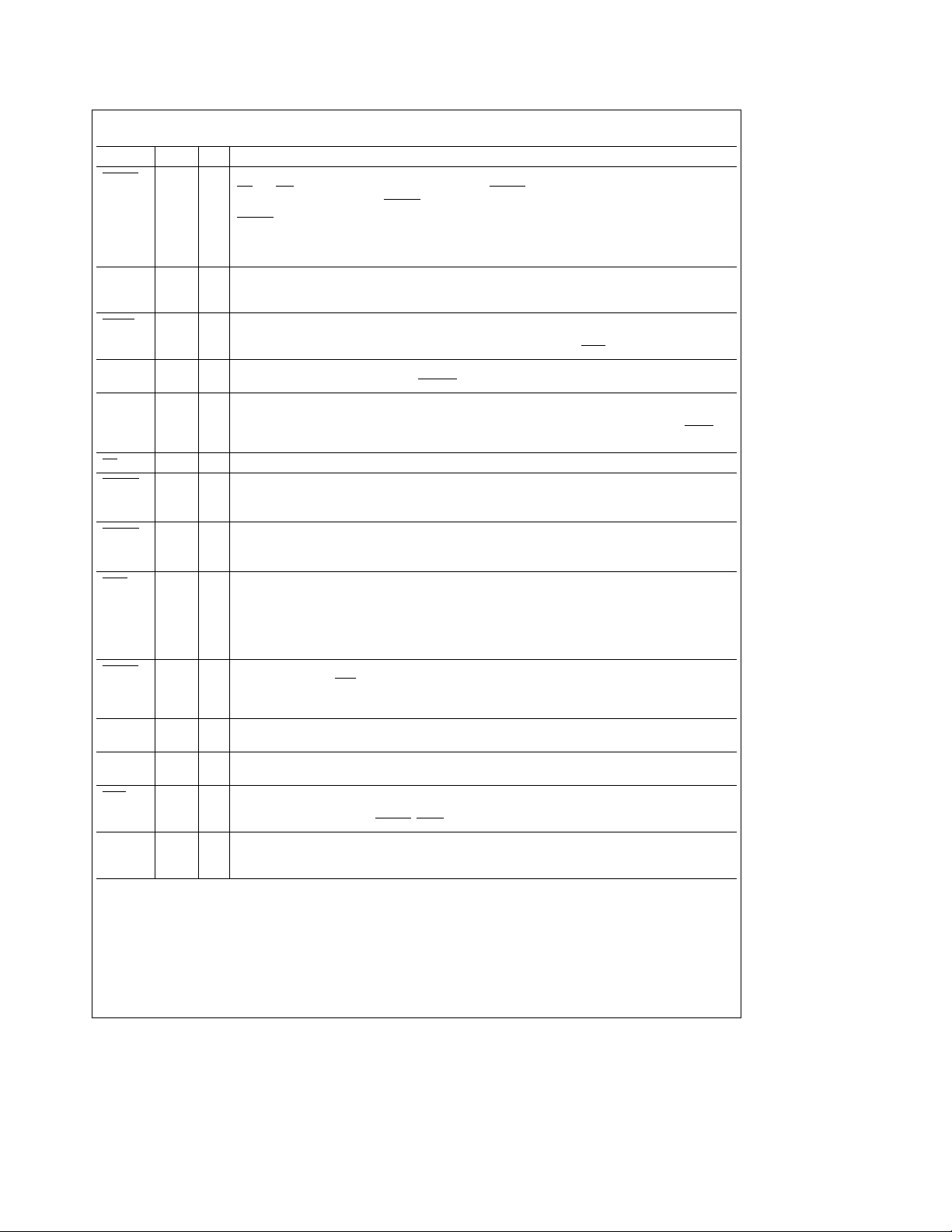
1.0 Pin Description (Continued)
Symbol Pin I/O Function
PDACK 54 I Printer DMA Acknowledge. Active low input to acknowledge the printer DMA request, and enable the
PDRQ 33 O Printer DMA Request. Active high output to signal the DMA controller that a printer data transfer is
PWDN 3IPower Down. This multi-function pin stops the clocks and/or the external crystal based on the
PE 83 I Paper End. This input is set high by the printer when it is out of paper. This pin has a nominal 25 k X
PNF 49 I Printer Not Floppy. PNF is the Printer Not Floppy pin when bit 2 of FCR is 1. It selects the device
RD 19 I Read. Active low input to signal data read by the microprocessor.
RDATA
Normal 35 I Read Data. This input is the raw serial data read from the floppy disk drive.
Mode
RDATA
PPM 91 I Read Data. This pin provides an additional Read Data signal in PPM Mode when PNFe0. (See PD3
Mode
RI1,2 70, 62 I Ring Indicator. When low this indicates that a telephone ring signal has been received by the MODEM.
RTS1,2 74, 66 O Request to Send. When low, this output indicates to the MODEM or data set that the UART is ready to
SIN1,2 75, 67 I Serial Input. This input receives composite serial data from the communications link (e.g. peripheral
SLCT 82 I Select. When a printer is connected, it sets this input high. This pin has a nominal 25 kX pull-down
SLIN 81 I/O Select Input. When this signal is low it selects the printer. This pin is in a TRI-STATE condition 10 ns
SOUT1,2 73, 65 O Serial Output. This output signal sends composite serial data to the communications link (e.g.
RD
and WR inputs during a DMA transfer. This pin is PDACK input pin when bit 3 of PMC is 1. It is
IDENT when bit 3 of PMC is 0. PDACK
is assumed to be 1 when bit 3 of PMC is 0.
PDACK
IDENT is assumed to be 1 when bit 3 of PMC is 1.
This input is valid only in ECP mode.
required. This pin is in TRI-STATE when ECP is disabled (bit 2 of PCR is 0), or configured with no DMA
(bit 3 of PMC is 0). This output is valid only in ECP mode.
selections made in the Power and Test Register bits 1-2. This pin also affects the FDC, UARTs, IDE
and Parallel Port pins, when the relevant PMC register bits are set. (See ZWS
pull-down resistor attached to it. (See WDATA
which is connected to the PPM pins. A parallel printer is connected when PNF
drive is connected when PNF
further information.)
and Table 7-5 for further information.)
The RI signal is a MODEM status input whose condition the CPU can test by reading bit 6 (RI) of the
MODEM Status Register (MSR) for the appropriate serial channel. Bit 6 is the complement of the RI
signal. Bit 2 (TERI) of the MSR indicates whether the RI input has changed from low to high since the
previous reading of the MSR.
Note: When the TERI bit of the MSR is set, an interrupt is generated if MODEM Status interrupts are enabled.
exchange data. The RTS
Control Register to a high level. A Master Reset operation sets this signal to its inactive (high) state.
Loop mode operation holds this signal to its inactive state. (See CFG0–4 for further information.)
device, MODEM, or data set).
resistor attached to it.
aftera0isloaded into the corresponding Control Register bit. The system should pull this pin high
using a 4.7 kX resistor. (See ASTRB
peripheral device, MODEM, or data set). The SOUT signal is set to a marking state (logic 1) after a
Master Reset operation. (See BOUT and CFG0–4 for further information.)
signal can be set to an active low by programming bit 1 (RTS) of the MODEM
input pin is ECP DMA acknowledge.
for further information.)
and Table 7-5 for further information.)
e
e
0. This pin is the DRV2 input pin when bit 2 of FCR is 0. (See DRV2 for
, STEP and Table 7-5 for further information.)
1, and a floppy disk
14
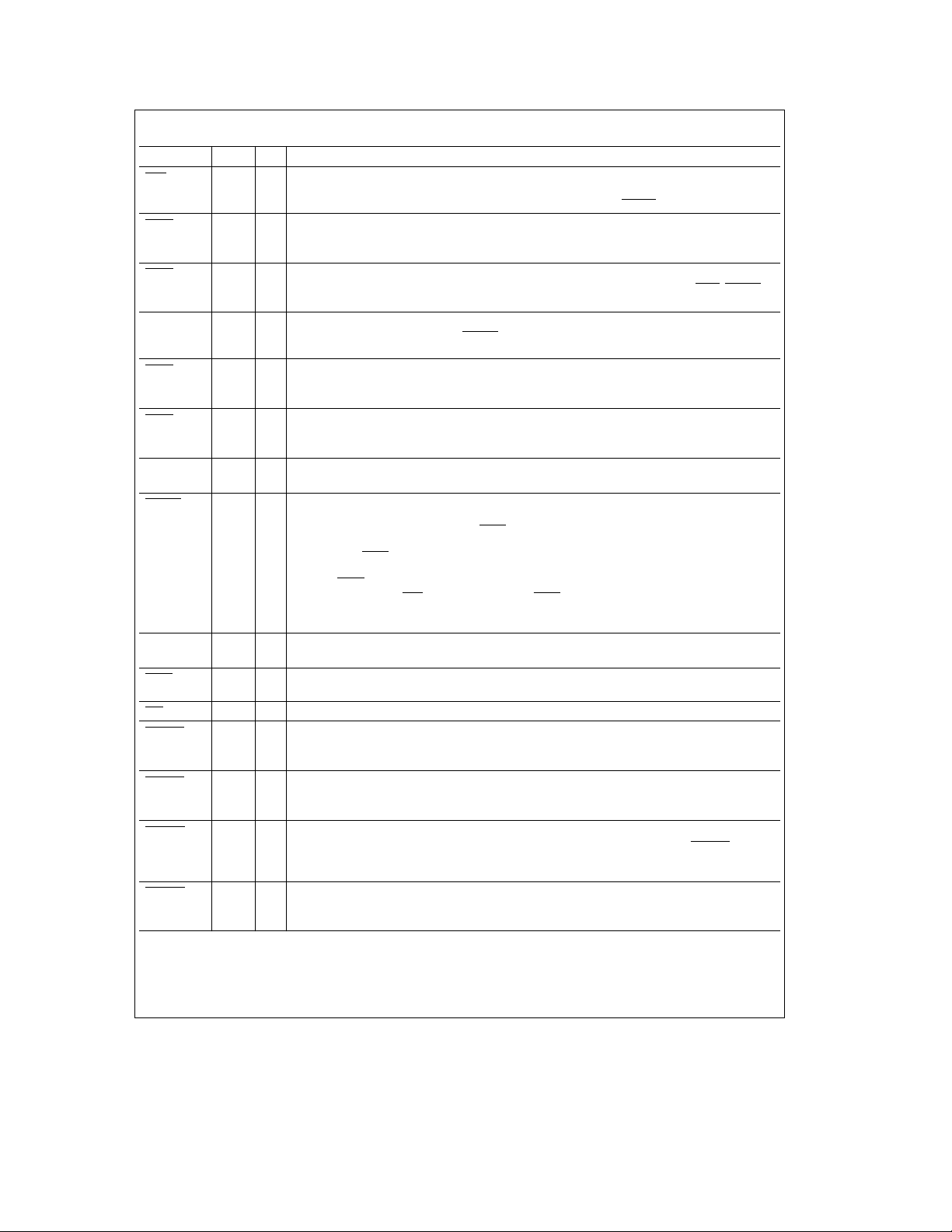
1.0 Pin Description (Continued)
Symbol Pin I/O Function
STB 95 I/O Data Strobe. This output signal indicates to the printer that valid data is available at the printer port.
STEP
Normal 40 O Step. This output signal issues pulses to the disk drive at a software programmable rate to move the
Mode
STEP
PPM 81 O Step. This pin provides an additional step signal in PPM Mode when PNFe0. (See SLIN, ASTRB
Mode
TC 6 I TerminaI Count. Control signal from the DMA controller to indicate the termination of a DMA
TRK0
Normal 37 I Track 0. This input indicates to the controller that the head of the selected floppy disk drive is at
Mode
TRK0
PPM 93 I Track 0. This pin provides an additional Track 0 signal in PPM Mode when PNFe0. (See PD1 and
Mode
V
, 50, 99 Power Supply. This is the 3.3V or 5V supply voltage for the PC87332 circuitry.
DDB
V
DDC
VLD0,1 56, 63 I Valid Data. These input pins are sensed during reset, and indicate the state of bit 5 in the FDC Tape
V
SSB,VSSC
V
SSD,VSSE
WAIT 84 I Wait. This signal is used, in EPP mode, by the parallel port device to extend its access cycle. It is
WR 18 I Write. Active low input signal to indicate a write from the microprocessor to the controller.
WDATA
WDATA
WGATE
WGATE
, 42, 9, Ground. This is the ground for the PC87332 circuitry.
90, 61
Normal 39 O Write Data. This output is the write precompensated serial data that is written to the selected floppy
Mode
PPM 83 O Write Data. This pin provides an additional Write Data signal in PPM Mode when PNFe0. (See PE
Mode
Normal 38 O Write Gate. This output signal enables the write circuitry of the selected disk drive. WGATE has
Mode
PPM 82 O Write Gate. This pin provides an additional Write Gate signal in PPM Mode when PNFe0. (See
Mode
This pin is in a TRl-STATE condition 10 ns aftera0isloaded into the corresponding Control Register
bit. The system should pull this pin high using a 4.7 kX resistor. (See WRlTE
head during a seek operation.
and Table 7-5 for further information.)
transfer. TC is accepted only when FDACK
modes, and active low in PS/2 mode.
track zero.
Table 7-5 for further information.)
Drive Register (3F3h). They indicate whether bits 6 and 7 of this register contain valid media ID
information for floppy drives 0 and 1. If VLD0
accessed, bit 5 of the Tape Drive Register is a 0 indicating that bits 6 and 7 contain valid media ID
information. If VLD0
Drive Register is a 1 indicating that bits 6 and 7 do not contain valid media ID information. The same
is true of VLD1
If bit 0 of FCR is 1, the VLD bits have no meaning. VLD0 value during reset is loaded into bit 0 of
FCR (to select between media sense or DRATE). A 30 kX internal pull-down resistor is on each pin.
Usea10kXresistor to pull these pins to high during reset.
active low. (See BUSY and Table 7-5 for further information.)
disk drive. Precompensation is software selectable.
and Table 7-5 for further information.)
been designed to prevent glitches during power up and power down. This prevents writing to the disk
when power is cycled.
SLCT and Table 7-5 for further information.)
is sensed high at reset, then whenever drive 0 is accessed, bit 5 of the Tape
relative to the media ID information for drive 1.
is active. TC is active high in PC-AT and Model 30
is sensed low at reset, then whenever drive 0 is
for further information.)
15
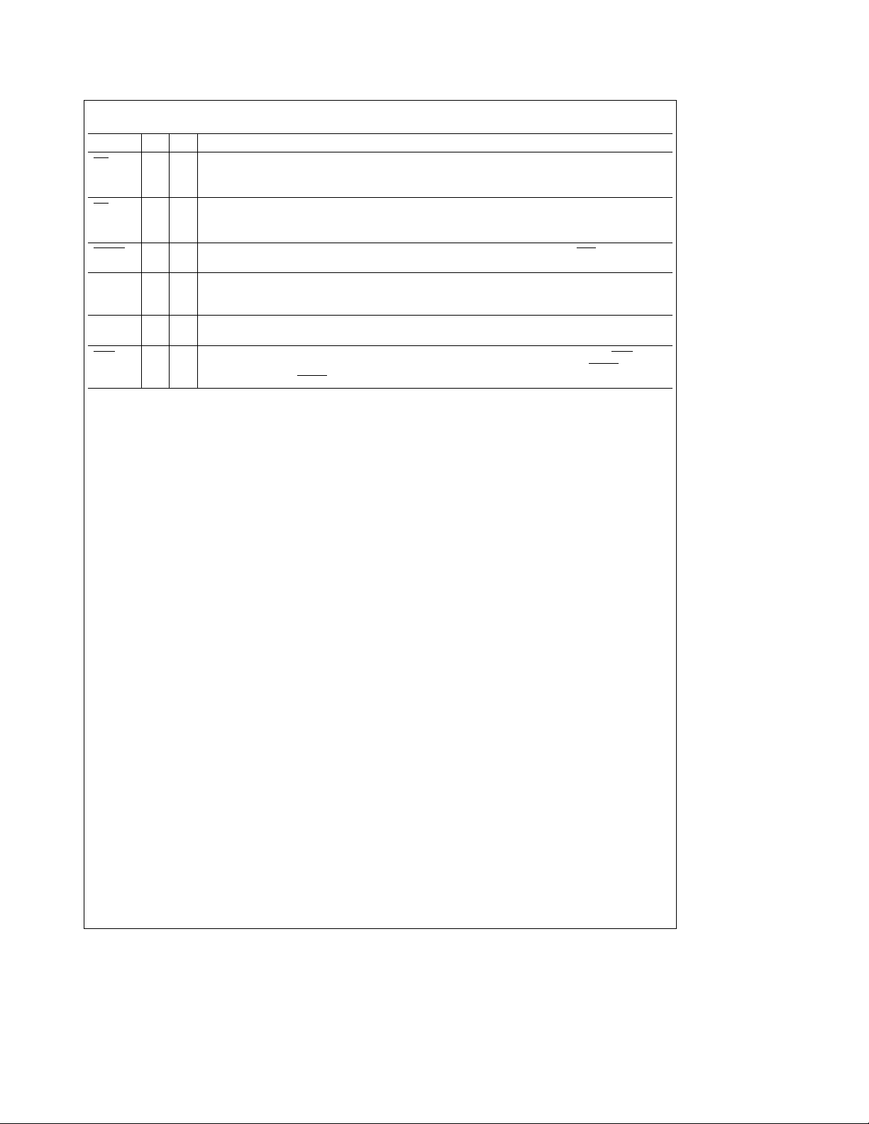
1.0 Pin Description (Continued)
Symbol Pin I/O Function
WP
Normal 36 I Write Protect. This input indicates that the floppy disk in the selected drive is write protected.
Mode
WP
PPM 92 I Write Protect. This pin provides an additional Write Protect signal in PPM Mode when PNFe0. (See
Mode
WRITE 95 O Write Strobe. This signal is used in EPP mode as a write strobe. It is active low. (See STB and Table 7-5
X1/OSC 7 I Crystal1/Clock. One side of an external 24 MHz/48 MHz crystal is attached here. The other side of the
X2 8 O Crystal2. One side of an external 24 MHz/48 MHz crystal is attached here. The other side of the crystal is
ZWS 3OZero Wait State. This pin is the Zero Wait State open drain output pin when bit 6 of FCR is 0. ZWS is
PD2 and Table 7-5 for further information.)
for further information.)
crystal is connected to X2. If a crystal is not used, a TTL or CMOS compatible clock is connected to this
pin.
connected to X1/OSC. This pin is left unconnected if an external clock is used.
driven low when the EPP or ECP is written, and the access can be shortened. This pin is PWDN
of FCR is 1. (See the PWDN
pin for further information.)
when bit 6
16

2.0 Configuration Registers
2.1 OVERVIEW
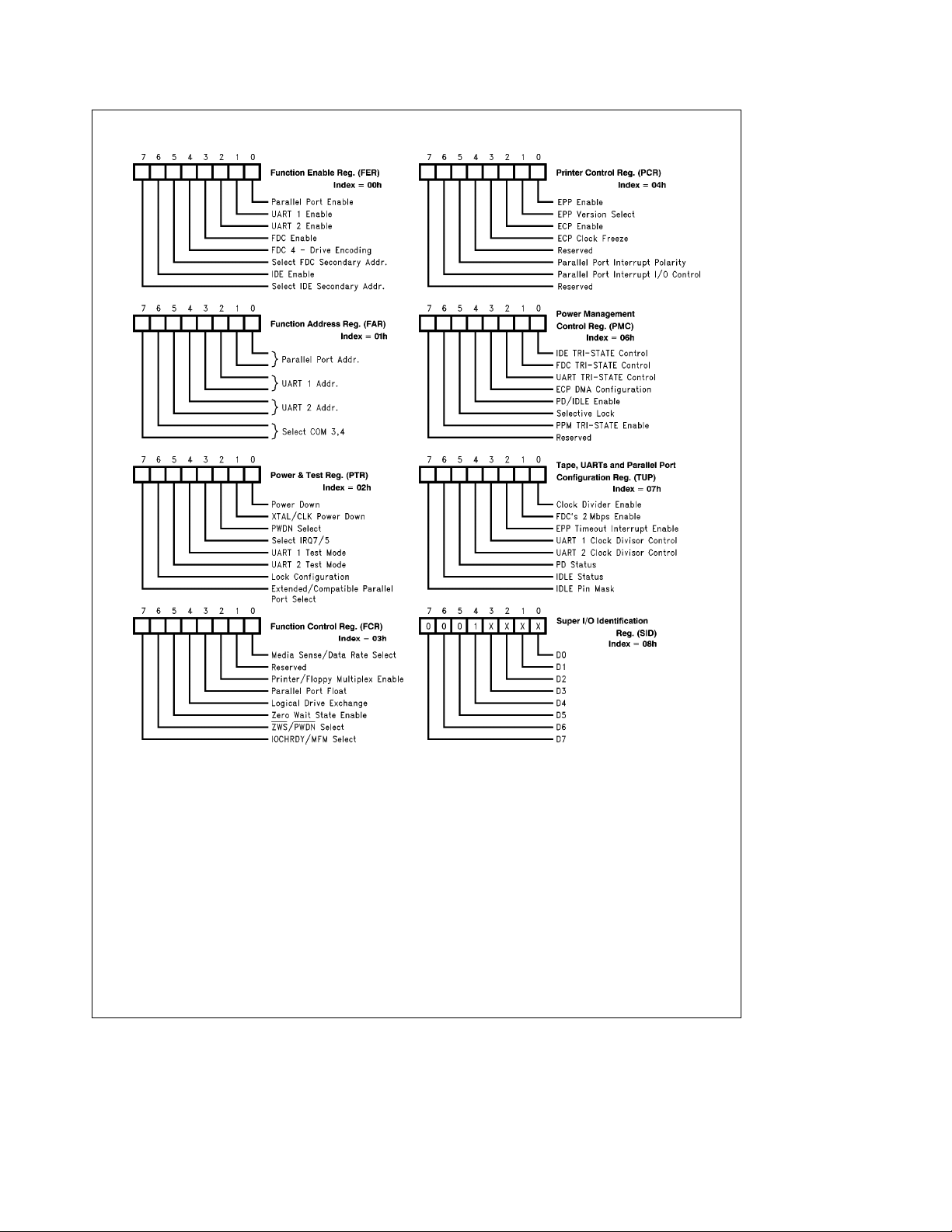
Eight registers constitute the Base Configuration Register
set, and control the PC87332 set-up. In general, these registers control the enabling of major functions (FDC, UARTs,
parallel port, pin functionality, etc.), the I/O addresses of
these functions, and whether they power-down via hardware control or not. These registers are the Function Enable
Register (FER), Function Address Register (FAR), Power
and Test Register (PTR), Function Control Register (FCR),
the Printer Control Register (PCR), the Power Management
Control Register (PMC), the Tape, UARTs and Parallel Port
Configuration Register (TUP), and the SuperI/O (SIO) Identification Register (SID).
During reset, the PC87332 loads a set of default values selected by a hardware strapping option into the FER, FAR,
and PTR Configuration Registers. The FCR, PCR, PMC,
TUP and SID registers can only be accessed by software.
An index and data register pair are used to read and write
the configuration registers. Each Configuration Register is
pointed to the value loaded into the Index Register. The
data to be written into the Configuration Register is transferred via the Data register. A Configuration Register is read
in a similar way (i.e., by pointing to it via the Index Register
and then reading its contents via the Data Register).
Accessing the Configuration Registers in this way requires
only two system I/O addresses. Since I/O address space is
shared by other devices, the Index and Data Registers can
still be inadvertently accessed. To reduce the chances of an
inadvertent access, a simple procedure has been developed. It is described in Section 2.2.
2.2 SOFTWARE CONFlGURATlON
If the system requires access to the Configuration Registers
after reset, the following procedure must be used to change
data in the registers.
1. Determine the default location of the PC87332 Index
Register.
Check the four possible locations (see Table 2-1) by
reading them twice. The first byte is the ID byte 88h, although read-after-write always brings the value of the
written byte. The second byte read is always 00h. Compare the data read with the ID byte and then 00h. A
match occurs at the correct location. Note that the ID
byte is only issued from the Index Register during the first
read after a reset. Subsequent reads return the value
loaded into the Index Register. Bits 4-6 are reserved and
always read 0.
2. Load the Configuration Registers.
A. Disable CPU interrupts.
B. Write the index of the Configuration Register (00h –
0Eh) to the Index Register one time.
C. Write the correct data for the Configuration Register in
two consecutive write accesses to the Data Register.
D. Enable CPU interrupts.
3. Load the Configuration Registers (read-modify-write).
A. Disable CPU interrupts.
B. Write the index of the Configuration Register (00h –
0Eh) to the Index Register one time.
C. Read the configuration data in that register via the
Data Register.
D. Modify the configuration data.
E. Write the changed data for the Configuration Register
in two consecutive writes to the Data Register. The
register updates on the second consecutive write.
F. Enable CPU interrupts.
A single read access to the Index and Data Registers can
be done at any time without disabling CPU interrupts. When
the Index Register is read, the last value loaded into the
Index Register is returned. When the Data Register is read,
the Configuration Register data pointed to by the Index Register is returned.
17
2.0 Configuration Registers (Continued)
FIGURE 2-1. PC87332VLJ/PC87332VLJ-5 Configuration Registers
18
TL/C/11930– 4

2.0 Configuration Registers (Continued)
2.3 HARDWARE CONFIGURATION
During reset, one of 32 possible sets of default values are
loaded into the first three Configuration Registers. A strapping option on five pins (CFG0 – 4) selects the set of values
that is loaded. This allows for automatic configuration without software intervention. Table 2-1 shows the 32 possible
default configurations. The default configuration can be
modified by software at any time after reset by using the
access procedure described in the Software Configuration
Section.
Table 2-1 is organized as follows. The logic values of the
five external Configuration Pins are associated with the resulting Configuration Register Data and the activated functions. The activated functions are grouped into seven categories based on the data in the FER. In some cases the
data in the FER is given as one of two options. This is because the primary or secondary IDE address is chosen via
the FER.
The PTR has one value associated with the active functions
in the FER. This value allows the power-down of all clocks
when the PWDN
functions are active after reset, activating the PWDN
also stops the crystal.
43210
00000FAR
00001FAR
00010FAR
00011FAR
00100FAR
00101FAR
00110FAR
00111FAR
01000FAR
01001FAR
01010FAR
01011FAR
01100FAR
01101FAR
01110FAR
01111FAR
pin goes active. In the last case where no
pin
TABLE 2-1. Default Configurations Controlled by Hardware
Configuration Pins (CFGn)
Most of the variability available is through the FAR. Addresses controlled by the FAR are coded as follows:
PRI: is the PRImary floppy or IDE address (i.e., 3F0–7h
SEC: is the SECondary IDE address (170–7, 376, 7h).
COM1: is the UART address at 3F8–Fh.
COM2: is the UART address at 2F8–Fh.
COM3: is the UART address at 3E8–Fh.
COM4: is the UART address at 2E8–Fh.
LPTA: is the parallel port (
LPTB: is the
The chosen addresses are given under active functions and
are in the same order as the active functions with which
they are associated. In other words, if the active functions
are given as FDC, IDE, UART1, UART2,
addresses are given as PRI, PRI, COM1, COM2, LPTB, then
the functions and the addresses are associated as follows:
FDC
UART2
Data
(Hex)
FERe4F, CF FDC, IDE, UART1, UART2,llPORT
PTRe00, 80 Power-Down Clocks Option
e
10 PRI, PRI, COM1, COM2, LPTB
e
11 PRI, PRI, COM1, COM2, LPTA
e
11 PRI, SEC, COM1, COM2, LPTA
e
39 PRI, PRI, COM3, COM4, LPTA
e
24 PRI, PRI, COM2, COM3, LPTB
e
38 PRI, SEC, COM3, COM4, LPTB
FERe4B, CB FDC, IDE, UART1,llPORT
PTRe00, 80 Power-Down Clocks Option
e
00 PRI, PRI, COM1, LPTB
e
01 PRI, PRI, COM1, LPTA
e
01 PRI, SEC, COM1, LPTA
e
09 PRI, PRI, COM3, LPTA
e
08 PRI, PRI, COM3, LPTB
e
08 PRI, SEC, COM3, LPTB
FERe0F FDC, UART1, UART2,llPORT
PTRe00, 80 Power-Down Clocks Option
e
10 PRI, COM1, COM2, LPTB
e
11 PRI, COM1, COM2, LPTA
e
39 PRI, COM3, COM4, LPTA
e
24 PRI, COM2, COM3, LPTB
or 1F0 – 7, 3F6, 7h).
3BEh.
PORT address at 378–37Fh.
ll
e
PRI, IDE
e
COM2,llPORTeLPTB.
e
PORT ) address at 3BC–
ll
PORT and the
ll
PRI, UART1
Activated Functions
e
COM1,
19

2.0 Configuration Registers (Continued)
TABLE 2-1. Default Configurations Controlled by Hardware (Continued)
Configuration Pins (CFGn)
43210
10000FAR
10001FAR
10010FAR
10011FAR
10100FAR
10101FAR
10110FAR
10111FAR
11000FAR
11001FAR
11010FAR
11011FAR
11100FAR
11101FAR
11110FAR
11111FAR
Data
(Hex)
FERe49, C9 FDC, IDE,llPORT
PTRe00, 80 Power-Down Clocks Option
e
00 PRI, PRI, LPTB
e
01 PRI, PRI, LPTA
e
01 PRI, SEC, LPTA
e
00 PRI, SEC, LPTB
FERe07 UART1, UART2,llPORT
PTRe00, 80 Power-Down Clocks Option
e
10 COM1, COM2, LPTB
e
11 COM1, COM2, LPTA
e
39 COM3, COM4, LPTA
e
24 COM2, COM3, LPTB
FERe47, C7 IDE, UART1, UART2,llPORT
PTRe00, 80 Power-Down Clocks Option
e
10 PRI, COM1, COM2, LPTB
e
11 PRI, COM1, COM2, LPTA
e
11 SEC, COM1, COM2, LPTA
e
39 PRI, COM3, COM4, LPTA
e
24 PRI, COM2, COM3, LPTB
e
38 SEC, COM3, COM4, LPTB
FERe08 FDC
PTRe00, 80 Power-Down Clocks Option
e
10 PRI
FERe00 None
PTRe02, 82 Power-Down XTAL and Clocks
e
10 NA
Activated Functions
20
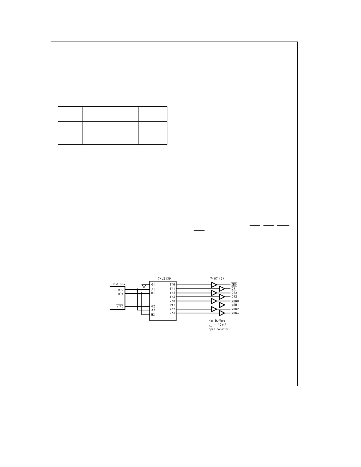
2.0 Configuration Registers (Continued)
2.4 INDEX AND DATA REGISTERS
Another general aspect of the Configuration Registers is
that the Index and the Data Register pair can be relocated
to one of four locations. This is controlled through a hardware strapping option on pins (BADDR0,1) and it allows the
registers to avoid conflicts with other adapters in the I/O
address space. Table 2-2 shows the address options.
TABLE 2-2. Index and Data Register
Optional Locations
BADDR1 BADDR0 Index Addr. Data Addr.
0 0 398 399
0 1 26E 26F
1 0 15C 15D
1 1 2E 2F
2.5 BASE CONFIGURATION REGISTERS
2.5.1 Function Enable Register (FER, Index 00h)
This register enables and disables major chip functions (e.g.
UARTs, parallel ports, FDC, etc.). Disabled functions have
their clocks automatically powered-down, but the data in
their registers remains intact. It also selects whether the
FDC and the IDE controller is located at their primary or
secondary address.
Bit 0 When this bit is 1 the parallel port can be accessed at
the address specified in the FAR.
Bit 1 When this bit is 1, UART1 can be accessed at the
address specified in the FAR. When this bit is 0, access to UART1 is blocked and it is in power-down
mode. The UART1 registers retain all data in powerdown mode.
Caution: Any UART1 interrupt that is enabled and
active or becomes active after UART1 is disabled,
asserts the associated IRQ pin. If disabling UART1
via software, clear the IRQ Enable bit (MCR3) to 0
before clearing FER 1. This is not an issue after reset
because MCR3 is 0 until it is written.
Bit 2 When this bit is 1, UART2 can be accessed at the
address specified in the FAR. When this bit is 0, access to UART2 is blocked and it is in power-down
mode. The UART2 registers retain all data in powerdown mode.
Caution: Any UART2 interrupt that is enabled and
active or becomes active after UART2 is disabled asserts the associated IRQ pin. If disabling UART2 via
software, clear the IRQ Enable bit (MCR3) to 0 before clearing FER 1. This is not an issue after reset
because MCR3 is 0 until it is written.
Bit 3 When this bit is 1, the FDC can be accessed at the
address specified in the FER bits. When this bit is 0
access to the FDC is blocked and it is in power-down
mode. The FDC registers retain all data in powerdown mode.
Bit 4 When this bit is 0 the PC87332 can control two floppy
disk drives directly without an external decoder.
When this bit is 1 the two drive select signals and two
motor enable signals from the FDC are encoded so
that four floppy disk drives can be controlled (see
Table 2-3 and
quires an external decoder. The pin states shown in
Table 2-3 are a direct result of the bit patterns shown.
All other bit patterns produce pin states that should
not be decoded to enable any drive or motor.
Bit 5 This bit selects the primary or secondary FDC ad-
dress. (See Table 2-4.)
Bit 6 When this bit is a 1 the IDE drive interface can be
accessed at the address specified by FER bit 7.
When it is 0, access to the IDE interface is blocked,
the IDE control signals (i.e., HCS0
IDEHI
signal is in TRI-STATE.
Bit 7 This bit selects the primary or secondary IDE ad-
dress. (See Table 2-4.)
Figure 2-2
) are held in the inactive state, and the IDED7
). Controlling four FDDs re-
, HCS1, IDELO,
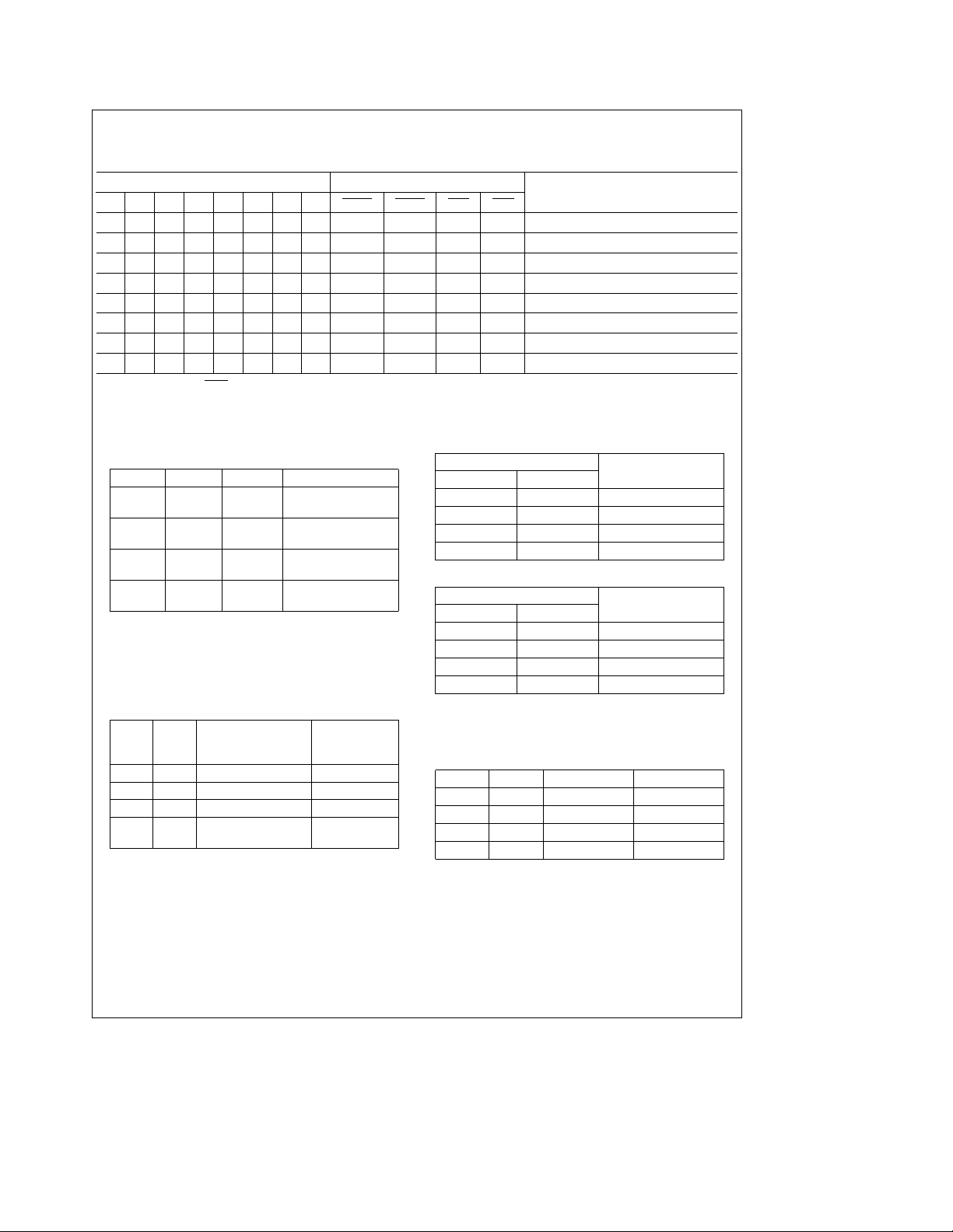
FIGURE 2-2. PC87332 Four Floppy Drive Circuit Example
21
TL/C/11930– 5
2.0 Configuration Registers (Continued)
TABLE 2-3. Encoded Drive and Motor Pin Information (FER 4
Digital Output Register Drive Control Pins
7 6 5 4 3 2 1 0 MTR1 MTR0 DR1 DR0
XXX1X X 0 0 (Note) 0 0 0 Activate Drive 0 and Motor 0
XX1X X X 0 1 (Note) 0 0 1 Activate Drive 1 and Motor 1
X 1 X X X X 1 0 (Note) 0 1 0 Activate Drive 2 and Motor 2
1 X X X X X 1 1 (Note) 0 1 1 Activate Drive 3 and Motor 3
XXX0X X 0 0 (Note) 1 0 0 Activate Drive 0 and Deactivate Motor 0
XX0X X X 0 1 (Note) 1 0 1 Activate Drive 1 and Deactivate Motor 1
X 0 X X X X 1 0 (Note) 1 1 0 Activate Drive 2 and Deactivate Motor 2
0 X X X X X 1 1 (Note) 1 1 1 Activate Drive 3 and Deactivate Motor 3
Note: When FER4e1, MTR1 presents a pulse that is the inverted image of the IOW strobe. This inverted pulse is active whenever an I/O write to address 3F2h
or 372h takes place. This pulse is delayed by 25 ns– 80 ns after the leading edge of IOW and its leading edge can be used to clock data into an external latch
(e.g., 74LS175). Address 3F2h is used if the FDC is located at the primary address (FER5
secondary address (FER5
e
1).
TABLE 2-4. Primary and Secondary
Drive Address Selection
Bit 5 Bit 7 Drive PC-AT Mode
0 X FDC Primary,
3F0–7h
1 X FDC Secondary,
3F0–7h
X 0 IDE Primary,
1F0–7h, 3F6 –7h
X 1 IDE Secondary
170–7h, 376 –7h
2.5.2 Function Address Register (FAR, Indexe01h)
This register selects the ISA I/O address range to which
each peripheral function responds.
Bits 0,1 These bits select the parallel port address as
shown in Table 2-5:
TABLE 2-5. Parallel Port Addresses
Bit1Bit
0
Parallel
Port
Address
PC-AT
Interrupt
*Note: COM3 and COM4 addresses are determined by Bits 6 and 7.
Bits 6,7 These bits select the addresses that are used for
0 0 LPTB (378 –37F) IRQ5 (Note)
0 1 LPTA (3BC –3BE) IRQ7
1 0 LPTC (278 –27F) IRQ5
1 1 Reserved TRI-STATE
Note: The interrupt assigned to this address can be changed to IRQ7 by
setting Bit 3 of the Power and Test Register (PTR).
(CTR4
e
0)
e
0) and address 372h is used if the FDC is located at the
TABLE 2-6. COM Port Selection for UART1
FAR UART1
Bit 3 Bit 2
0 0 1 (3F8-F)
0 1 2 (2F8-F)
1 0 3 (Table 2-8)*
1 1 4 (Table 2-8)*
TABLE 2-7. COM Port Selection for UART2
FAR UART2
Bit 5 Bit 4
0 0 1 (3F8-F)
0 1 2 (2F8-F)
1 0 3 (Table 2-8)*
1 1 4 (Table 2-8)*
COM3 and COM4 (see Table 2-8).
TABLE 2-8. Address Selection for COM3 and COM4
Bit 7 Bit 6 COM3 IRQ4 COM4 IRQ3
0 0 3E8–Fh 2E8–Fh
0 1 338–Fh 238–Fh
1 0 2E8–Fh 2E0–7h
1 1 220–7h 228–Fh
Bits 2–5 These bits determine which ISA I/O address range
is associated with each UART (see Table 2-6 and
Table 2-7).
e
1)
Decoded Functions
COM
COM
Ý
Ý
22

2.0 Configuration Registers (Continued)
2.5.3 Power and Test Register (PTR, Index
This register determines the power-down method used
when the power-down pin (PWDN
) is asserted (crystal and
clocks vs. clocks only) and whether hardware power-down
is enabled. It also provides a bit for software power-down of
all enabled functions. It selects whether IRQ7 or IRQ5 is
associated with LPTB. It puts the enabled UARTs into their
test mode.
Independent of this register the floppy disk controller can
enter low power mode via the Mode Command or the Data
Rate Select Register.
Bit 0 Setting this bit causes all enabled functions to be
powered-down.
If the crystal power-down option is selected (see Bit 1)
the crystal is also powered-down. All register data is
retained when the crystal or clocks are stopped. The
FDC, UARTs, IDE and Parallel Port pins are affected
by this bit when the relevant PMC register bits are set.
Note: Bits 2 and 3 of PCR can affect the function of the parallel port
power-down mode.
Bit 1 When the Power-Down pin or Bit 0 is asserted this bit
determines whether the enabled functions have their
internal clocks stopped (Bit 1
crystal (Bit 1
e
1) is stopped. Stopping the crystal is
the lowest power consumption state of the part. However, if the crystal is stopped, a finite amount of time
(E8 ms) is required for crystal stabilization once the
Power-Down pin (PWDN
) or Bit 0 is deasserted. If all
internal clocks are stopped, but the crystal continues
to oscillate, no stabilization period is required after the
Power-Down pin or Bit 0 is deasserted.
Bit 2 Reserved. This bit must be set to 0.
Bit 3 Setting this bit associates the parallel port with IRQ7
when the address for the parallel port is 378–37Fh
(LPTB). This bit is a ‘‘don’t care’’ when the parallel
port address is 3BC –3BEh (LPTA) or 278 –27Fh
(LPTC).
Bit 4 Setting this bit puts UART1 into a test mode, which
causes its Baud Out clock to be present on its SOUT1
pin if the Line Control Register bit 7 is set to 1.
Bit 5 Setting this bit puts UART2 into a test mode, which
causes its Baud Out clock to be present on its SOUT2
pin if the Line Control Register bit 7 is set to 1.
Bit 6 Setting this bit to 1 prevents all further write accesses
to the Configuration Registers. Once it is set by software it can only be cleared by a hardware reset. After
the initial hardware reset it is zero.
Bit 7 When not in EPP or ECP modes, this bit selects Com-
patible or Extended mode operation and thus controls
whether Pulse or Level interrupts are used.
Set this bit to 0 for Compatible mode, Pulse interrupt.
Set this bit to 1 for Extended mode, Level interrupt.
In EPP mode this bit selects Regular or Automatic
bidirectional mode, thus determining the direction
control method:
Set this bit to 0 for Automatic mode, Host RD
signals control the direction.
Set this bit to 1 for Regular mode, bit 5 of CTR controls the direction.
After the initial hardware reset, this bit is 0.
e
02h)
e
0) or the external
and WR
2.5.4 Function Control Register (FCR, Index
e
03h)
This register determines several pin options:
It selects between Data Rate output and automatic media
sense inputs.
It enables the Parallel Port Multiplexor (PPM), and switches
between internal and external drives.
For Enhanced Parallel Port operation it enables the
IOCHRDY and ZWS
options, and pins.
On reset bits 2–7 of FCR are cleared.
Bit 0 Media Sense/Data Rate select bit. When this bit is 0,
the MSEN0–1 pins are Media Sense inputs and bits
5–7 of TDR are valid. When this bit is 1, the
DRATE0–1 pins are Data Rate outputs and bits 2 – 7
of TDR are TRI-STATE during read. On reset, the
VLD0
pin is sampled and its value placed into this bit.
Bit 1 Reserved.
Bit 2 Printer/Floppy Parallel Port Multiplexor (PPM) enable
bit. When this bit is 0, the port is configured as a parallel port. When this bit is 1, the port is configured as a
floppy drive port. See PNF pin description for further
information. The DRV2
/PNF pin is read as DRV2 bit,
regardless of bit 2 of FCR.
Bit 3 Parallel Port Multiplexor (PPM) float control bit. When
this bit is 0, the PPM pins are driven. When this bit is
1, the PPM pins are in TRI-STATE mode and the pullups are disconnected.
Bit 3 is functional whether or not the PPM is configured (when bit 2 of FCR is 0).
When bit 3
e
1 the PPM outputs are in TRI-STATE
and the inputs are blocked to reduce their leakage
current. The values of the blocked inputs are:
e
BUSY
1, PEe0, SLCTe0, ACKe1 and ERRe1.
Note: To avoid undefined FDC inputs the PPM can be disabled be-
fore this bit is set.
Bit 4 Logical Drive Exchange bit. This bit allows software to
exchange the physical floppy-disk control signals, assigned to drives 0 and 1, thus exchanging the logical
drives A and B.
This is accomplished by exchanging control of the
DR0
and MTR0 pins with the DR1 and MTR1 pins.
The result is undefined if four drive mode is selected
e
(FER4
1). Table 2-9 shows the associations between the Configuration Register bit, the Digital Output Register bits (DRVSEL0,1 and MTR0,1) and the
drive and motor control pins (DR0,1
and MTR0,1).
TABLE 2-9. Logical Drive Exchange
FCR Digital Output Register (FDC)
Bit 4
MTR1 MTR0 DRVSEL1 DRVSEL0
Asserted
FDC Pins
0 0 1 0 0 DR0,
MTR0
0 1 0 0 1 DR1,
MTR1
1 0 1 0 0 DR1,
MTR1
1 1 0 0 1 DR0,
MTR0
23

2.0 Configuration Registers (Continued)
Bit 5 Zero Wait State enable bit. If this bit is 1, (and pin 3/1
(PQFP/TQFP) is configured as ZWS
low when the Enhanced Parallel Port (EPP) or the
ECP can accept a short host read/write-cycle, otherwise the ZWS
ZWS
operation should be configured when the sys-
open drain output is not driven. EPP
tem is fast enough to support it.
Bit 6 ZWS
/PWDN select bit. When this bit is 0, the ZWS
pin is Zero Wait State output.
When this bit is 1, the PWDN
selected.
Bit 7 IOCHRDY/MFM select bit. When this bit is 0, the
IOCHRDY pin is the IOCHRDY open drain output that
extends the host-EPP cycle when required.
When this bit is 1, the MFM pin is selected.
2.5.5 Printer Control Register (PCR, Index
This register enables the EPP, ECP, version modes, and
interrupt options. On reset all the PCR bits are cleared to 0.
The parallel port mode is software configurable as follows:
TABLE 2-10. Parallel Port Mode
Operation FER PTR PCR PCR
Mode Bit 0 Bit 7 Bit 0 Bit 2
None 0 X X X
Compatible 1000
Extended 1100
EPP 1 X 1 0
ECP 1 X 0 1
Bit 0 EPP enable bit. When this bit is 0, the EPP is disabled,
and the EPP registers are not accessible (access ignored).
When this bit is 1, and bit 2 of PCR is 0, the EPP is
enabled. Note that the EPP should not be configured
with base address 3BCh.
Bit 1 EPP version select bit. When this bit is 0, Version 1.7 is
supported.
When this bit is 1, Version 1.9 is supported (IEEE
1284).
Bit 2 ECP enable bit. When this bit is 0, the ECP is disabled
and in power mode. The ECP registers are not accessible (access ignored), the ECP interrupt is inactive
and the DMA request pin is in TRI-STATE. The IRQ5,7
inputs are blocked to reduce their leakage currents.
When this bit is 1, the ECP is enabled. The software
should change this bit to 1 only when bits 0, 1, and 2 of
the existing CTR are 1, 0, and 0 respectively.
Bit 3 ECP Clock Freeze Control Bit. In power-down modes
2 and 3: When this bit is 0, the clock provided to the
ECP is stopped; and
When this bit is 1, the clock provided to the ECP is not
stopped.
Note: When either this bit or the ECP enable bit is 0, there is no
change in the PC87334 crystal stopping mechanism.
Bit 4 Reserved. This bit must be set to 0.
Bit 5 Parallel port interrupt (IRQ5 or IRQ7) polarity control
bit.
) ZWS is driven
/CSOUT pin option is
e
04h)
When this bit is 0, the interrupt polarity is as already
defined, and the ECP interrupt is level high or negative pulse.
When this bit is 1, the interrupt polarity is inverted.
Bit 6 Parallel port interrupt (IRQ5 or IRQ7) open drain con-
trol bit.
When this bit is 0, the configured interrupt line (IRQ5
or IRQ7) has a totem-pole TRI-STATE output.
When this bit is 1, the configured interrupt line has an
open drain output (drive low or TRI-STATE, no drive
high, no internal pullup).
Bit 7 Reserved. To maintain compatibility with future
SuperI/O devices, this bit must not be modified when
this register is written. Use read-modify-write to preserve the value of this bit.
2.5.6 Power Management Control Register
(PMC, Index
e
06h)
This register controls the TRI-STATE and input pins. The
PMC Register is accessed through Index 06h. The PMC
Register is cleared to 0 on reset.
Bit 0 IDE TRI-STATE control bit. When this bit is 1, and ei-
ther the IDE is disabled or the SuperI/O is in powerdown mode, HCS0
and HCS1 are in TRI-STATE.
IDED7 input is also blocked to reduce leakage current
and its value is undefined when IDE is disabled.
Bit 1 FDC TRI-STATE control bit. When this bit is 1 and the
FDC is powered-down, the FDC outputs are in TRISTATE (except IRQ6, PD, IDLE and the PPM outputs,
even if the PPM is used as FDC pins), and the FDC
inputs (except DSKCHG
) are blocked to reduce their
leakage current.
Bit 2 UARTs TRI-STATE control bit. When this bit is 1, and
any UART is powered-down, the outputs of that UART
are in TRI-STATE (except IRQ3 and IRQ4), and the
inputs are blocked to reduce their leakage current.
The values of the blocked inputs are: SIN
e
DSR
1, DCDe1 and RIe1.
e
1, CTSe1,
Bit 3 ECP DMA configuration bit. When this bit is 0, ECP
DMA is not configura ble: IDENT/PDACK
is assumed
to be 1 and PDRQ is in TRI-STATE.
When this bit is 1, ECP DMA is configurable via an
ECP control register. Pins 54 and 33 are PDACK
and
PDRQ respectively. IDENT is assumed to be 1.
Note: This bit must not be set when the PC87332 is assembled into a
PC87312/PC87322 socket, in which pin 33 is V
A.
DD
Bit 4 PD and IDLE (FDC power management output pins)
enable bit.
When this bit is 0, pins 43 and 45 are MTR1
and DR1
respectively.
When this bit is 1, pins 43 and 45 are IDLE and PD
respectively.
Bit 5 Selective Lock bit. This bit enables locking of the fol-
lowing configuration bits: bit 5 of PMC, bit 4 of FER,
bits 0 –7 of FAR, bits 2 – 3 of PTR, bits 6–7 of FCR,
and bit 0 of TUP. Unlike bit 6 of PTR, it does not lock
all the configuration bits.
Once this bit is set by software it can only be cleared
by a hardware reset. This bit should be used instead of
bit 6 of PTR if a configuration bit should be dynamically
modified by software (like PMC bits).
24

2.0 Configuration Registers (Continued)
When this bit is 0, bit 6 of PTR can be used to lock all
configuration registers.
When this bit is 1, the above configuration bits cannot
be modified. A hardware reset clears this bit.
Bit 6 Parallel Port Multiplexor (PPM) TRI-STATE enable bit.
This bit enables reduction in power consumption,
(when the SuperI/O is in power-down mode or the parallel port is disabled) by placing the PPM outputs in
TRI-STATE, and blocking the PPM inputs.
When this bit is 0, the parallel port pins are enabled.
When this bit is 1, and either the parallel port is disabled or the SuperI/O is in power-down mode, the outputs of the Parallel Port, pins (except IRQ5 and IRQ7)
are in TRI-STATE, and the inputs are blocked to reduce their leakage currents.
The values of the blocked inputs are: BUSY
e
PE
0, SLCTe0, ACKe1 and ERRe1.
Bit 7 Reserved. To maintain compatibility with future
SuperI/O devices, this bit must not be modified when
this register is written. Use read-modify-write to preserve the value of this bit.
2.5.7 Tape, UARTs and Parallel Port Configuration
Register (TUP, Index
e
07h)
The TUP Register is cleared to 0XX0000X on reset.
Bit 0 CLK48. Clock divider enable bit.
When a 48 MHz clock is used this bit should be 1.
When a 24 MHz clock is used this bit should be 0.
When this bit is 0, the clock for all the PC87332 modules is X1/OSC (i.e., 24 MHz).
When this bit is 1, the clock of all PC87332 modules,
except the FDC, is X1/OSC divided by 2 (i.e., 48/2
24 MHz), and the FDC clock depends on bit 1 of TUP.
During reset the value of CLK48 pin (pin 57) is latched
into this bit.
This bit should not be modified by the user.
Bit 1 FDC’s 2 Mbps enable bit.
When this bit is 0, a 2 Mbps data rate is not supported
by the FDC, and the FDC clock is 24 MHz (X1/OSC
when bit 0 of TUP is 0, or X1/OSC divided by 2 when
bit 0 of TUP is 1).
When this bit is 1, 2 Mbps is supported by the FDC,
and the FDC clock is 48 MHz (X1/OSC when bit 0 of
TUP is 1). Bit 0 of TUP must be set to 1, and a 48 MHz
clock must be used to support a 2 Mbps data rate. The
operating voltage should be 5V. (See Section 5.0 FDC
Functional Description.)
Bit 2 EPP Timeout Interrupt Enable bit.
When this bit is 0, the EPP timeout interrupt is masked.
When this bit is 1, the EPP timeout interrupt is generated on the selected IRQ line (IRQ5 or IRQ7), according
to PCR 6.
Bit 3 UART 1 clock divisor control (MIDI baud rate configu-
ration) bit.
When this bit is 0, the UART 1 Baud Rate Generator is
fed by the master clock divided by 13.
When this bit is 1, the UART 1 Baud Rate Generator is
fed by the master clock divided by 12. This bit should
be set to 1 to support MIDI baud rates.
e
Bit 4 UART 2 clock divisor control (MlDI baud rate configu-
ration) bit.
When this bit is 0, the UART 2 Baud Rate Generator is
fed by the master clock divided by 13.
When this bit is 1, the UART 2 Baud Rate Generator is
fed by the master clock divided by 12. This bit should
be set to 1 to support MIDI baud rates.
Bit 5 PD status bit. This bit holds the FDC power-down
state, as defined for the PD pin, even when pin 45 is
not configured as PD. This bit is read only.
Bit 6 IDLE status bit. This bit holds the FDC idle state, as
defined for the IDLE pin, even when pin 43 is not configured as IDLE, and when IDLE is masked by bit 7 of
TUP. This bit is read only.
Bit 7 IDLE pin mask bit. This bit masks the IDLE output pin
(but not the IDLE status bit). This bit is ignored when
1,
pin 43 is not configured as idle.
When this bit is 0, the IDLE output pin is unmasked.
The IDLE pin drives the value of the FDC idle state.
When this bit is 1, the IDLE output pin is masked. The
IDLE pin is driven low.
2.5.8 SuperI/O Identification Register
(SID, Index
e
08h)
The SID Register is accessed, like the other configuration
registers, through the Index Register. This read-only register
is used to identify the PC87332 device.
765432 10
0 0 0 1 X X X X Super I/O Identification
e
2.6 POWER-DOWN OPTIONS
The PC87332 places special emphasis on power manage-
Reg. (SID)
Index
e
08h
ment. Power management methods can be divided into two
major groups:
Group 1: Full device power-downÐthe entire PC87332
SuperI/O is powered-down and thus disabled.
Group 2: Specific function power-downÐspecific SuperI/O
modules (FDC, UART1, UART2, IDE, ECP or Par-
allel Port) are powered-down and thus disabled.
All power-down modes are enhanced by a new feature
which allows the output pins associated with a specific function (FDC, UART1, UART2, IDE, Parallel Port) to be TRISTATE pins, and reduces current leakage by blocking their
inputs.
Four modules in the PC87332 are operated by the internal
clockÐFDC, UART1, UART2 and ECP. These modules can
be powered-down or disabled by stopping their associated
internal clocks. In addition, all four modules can be
powered-down or disabled by stopping the external crystal
oscillator.
Modules which do not use a clock, the IDE and Parallel Port
(SPP/EPP), can be powered-down or disabled by simply
blocking access to them.
All the above power-down modes can be achieved using
the power-down methods from Group 1 or Group 2, as described in the following sections.
25

2.0 Configuration Registers (Continued)
2.6.1 Recommended Power-Down MethodsÐGroup 1
Use the power-down methods in Group 1 to place the
PC87332 in one of the following modes:
Mode 1: The entire chip is powered-down, the crystal osci-
IIator is stopped, pins are TRI-STATE and the inputs are blocked.
In this mode the maximum current saving can be
achieved.
Mode 2: The entire chip is powered-down, the crystal os-
cillator is stopped. Pins are driven.
Mode 3: The entire chip is powered-down, pins are TRI-
STATE, and the inputs are blocked. The crystal
oscillator operates, and provides fast wake-up.
Mode 4: The entire chip is powered-down. Pins are driven.
The crystal oscillator operates.
There are 13 methods to reach the above four operating
modes. See Table 2-11.
2.6.2 Recommended Power-Down MethodsÐGroup 2
Use the power-down modes in Group 2 to place the
PC87332 in any desired combination of the following powerdown modes:
Mode 1: Parallel Port (SPP/EPP/ECP) is powered-down,
providing a savings of up to 5 mA.
Mode 2: UARTs are powered-down providing a savings of
up to 5 mA.
2.7 POWER-UP PROCEDURE AND CONSIDERATIONS
2.7.1 Crystal Stabilization
If the crystal is stopped by putting either the FDC or both
UARTs into low power mode, then a finite amount of time
(E8 ms) must be allowed for crystal stabilization during
subsequent power-up. The stabilization period can be
sensed by reading the Main Status Register in the FDC, if
the FDC is being powered up. (The Request for Master bit is
not set forE8 ms.) If either one of the UARTs are being
powered up, but the FDC is not, then the software must
determine theE8 ms crystal stabilization period. Stabilization of the crystal can also be sensed by putting the UART
into local loopback mode and sending bytes until they are
received correctly.
2.7.2 UART Power-Up
The clock signal to the UARTs is controlled through the
Configuration Registers (FER, PTR). In order to restore the
clock signal to one or both UARTs the following conditions
must exist:
1. The appropriate enable bit (FER1,2) for the UART(s)
must be set.
2. The Power-Down bit (PTR0) must not be set.
3. If the PWDN pin option (PTR2 and FCR6) is used the
CSOUT
/PWDN/ZWS pin must be inactive.
If the crystal has been stopped follow the guidelines in
Section 2.7.1 before sending data or signaling that the receiver channel is ready.
Mode 3: FDC is powered-down, providing a savings of up
to 4 mA.
Mode 4: IDE is powered-down, providing a savings of up
to 0.1 mA.
See also the PMC register.
TABLE 2-11. Methods to Achieve Group 1 Power-Down Modes
Method PTR Bits 012
Pin 3
(Note 3)
FER Bits 01236 PCR Bit 2 PMC Bits 0126 Mode
1 11x x xxxxx x 1111
2 x10 0 xxxxx x 1111
3 x1x x 00000 0 1111
4 11x x xxxxx x 0000
5 x10 0 xxxxx x 0000
6 x1x x 00000 0 0000
7 x1x x xxx1x x 0000 (Notes 1, 2)
8 10x x xxxxx x 1111
9 x00 0 xxxxx x 1111
10 x0x x 00000 0 1111
11 10x x xxxxx x 0000
12 x00 0 xxxxx x 0000
13 x0x x 00000 0 0000 (Note 1)
Note 1: The PC87332 can also be placed in Mode 2, or Mode 4, using the strap configuration pins CFG0– 4 (see Table 2-1).
Note 2: The PC87332 can also be placed in Mode 2 by using method
high.
Ý
Note 3: Pin
Note 4: These values are measured under the following conditions:
Note 5: UARTS should be in 16550 (FIFO) mode; bit 0 of FIFO Control Register should be 1.
3 is PDWN input (configured when bit 2 of PTR is 0 and bit 6 of FCR is 1).
1. No load on outputs
2. Inputs are stable
e
3. V
IL
4. V
DD
5. Using a crystal for the 24 MHz clock.
VSS,V
e
3.3V
e
V
IH
DD
Ý
7, and entering FDC Low Power by executing Mode Command or by setting bit 6 of DSR to
26
Typical Current
Consumption
(Notes 4, 5)
Ý
110mA
Ý
230mA
Ý
34mA
Ý
44mA
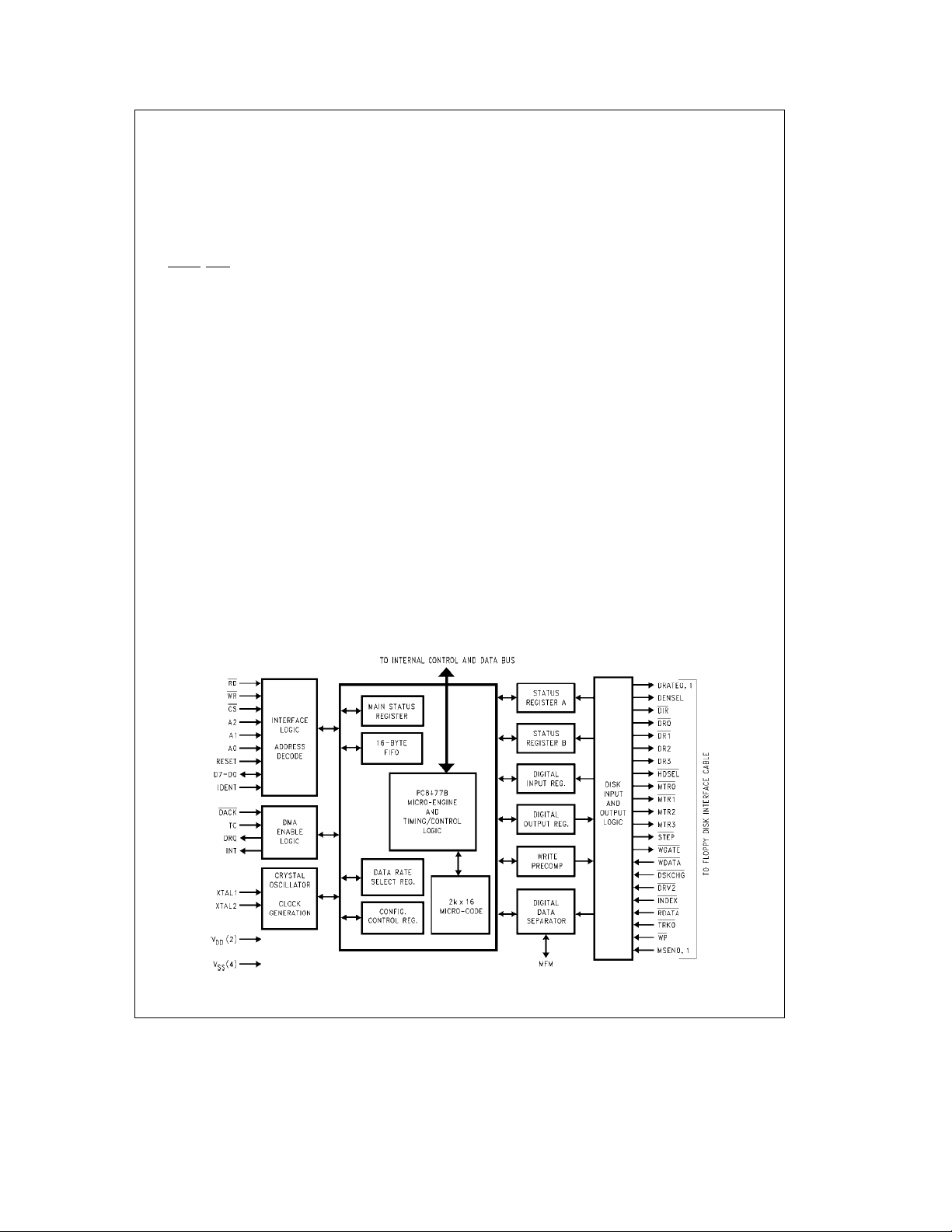
2.0 Configuration Registers (Continued)
2.7.3 FDC Power-Up
The clock signal to the FDC is controlled through the Configuration Registers, the FDC Mode Command and the Data
Rate Select Register. In order to restore the clock signal to
the FDC the following conditions must exist:
1. The appropriate enable bit (FER3) must be set.
2. The Power-Down bit (PTR0) must not be set.
3. If the PWDN pin option (PTR2 and FCR 6) is used, the
PWDN
/ZWS pin must be inactive.
In addition to these conditions, one of the following actions
must be taken to initiate recovery from the Power-Down
mode:
1. Read the Main Status Register until the RQM bit (MSR7)
is set OR
2. Write to the Data Rate Select Register and set the Software Reset bit (DSR7) OR
3. Write to the Digital Output Register, clear and then set
the Reset bit (DOR2) OR
4. Read the Data Register and the Main Status Register
until the RQM bit is set.
If the crystal has been stopped, read the RQM bit in the
Main Status Register until it is set. The RQM bit is not set
until the crystal has stabilized.
3.0 FDC Register Description
The floppy disk controller (FDC) is suitable for all PC-AT,
EISA, PS/2, and general purpose applications. The operational mode (PC-AT, PS/2, or Model 30) of the FDC is determined by hardware strapping of the IDENT and MFM pins.
DP8473 and N82077 software compatibility is provided. Key
features include a 16-byte FIFO, PS/2 diagnostic register
support, perpendicular recording mode, CMOS disk interface, and a high performance digital data separator. See
Figure 3-1
.
The FDC supports fast 2 Mbps data rate drives and standard 1 Mbps, 250/500 kbps and 300/500 kbps data rate
drives. The 1 Mbps data rate is used by the high performance tape and floppy disk drives. The 2 Mbps data rate is
used in very high performance tape drives. The FDC also
supports the perpendicular recording mode, a new format
used with some high performance, high capacity disk drives
at the 1 Mbps data rate.
The high performance internal digital data separator needs
no external components. It improves on the window margin
performance standards of the DP8473, and is compatible
with the strict data separator requirements of floppy disk
and floppy-tape drives.
The FDC contains write precompensation circuitry that defaults to 125 ns for 250 kbps, 300 kbps, and 500 kbps, to
41.67 ns for 1 Mbps and to 20.8 ns for 2 Mbps. These
values can be overridden in software to disable write precompensation or to provide levels of precompensation up to
250 ns.
The FDC has internal 24 mA data bus buffers which allow
direct connection to the system bus. The internal 40 mA
totem-pole disk interface buffers are compatible with both
CMOS drive inputs and 150X resistor terminated disk drive
inputs.
3.1 FDC CONTROL REGISTERS
The following FDC registers are mapped into the addresses
shown in Table 3-1 and described in the following sections.
The base address range is provided by the on-chip address
decoder pin. For PC-AT or PS/2 applications, the diskette
controller primary address range is 3F0h to 3F7h, and the
secondary address range is 370h to 377h. The FDC supports three different register modes: the PC-AT mode, PS/2
mode (MicroChannel systems), and the Model 30 mode.
See Section 5.2 for more details on how each register mode
is enabled. When applicable, the register definition for each
mode of operation is given.
If no special notes are made, then the register is valid for all
three register modes.
FIGURE 3-1. FDC Functional Block Diagram
27
TL/C/11930– 6
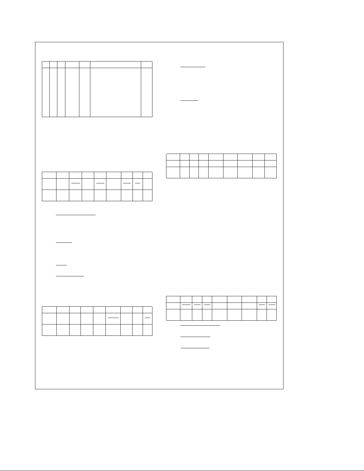
3.0 FDC Register Description (Continued)
TABLE 3-1. Register Description and Addresses
A2 A1 A0 IDENT R/W Register
0 0 0 0 R Status Register A* SRA
0 0 1 0 R Status Register B* SRB
0 1 0 X R/W Digital Output Register DOR
0 1 1 X R/W Tape Drive Register TDR
1 0 0 X R Main Status Register MSR
1 0 0 X W Data Rate Select Register DSR
1 0 1 X R/W Data Register (FIFO) FIFO
1 1 0 X X None (Bus TRI-STATE)
1 1 1 X R Digital Input Register DIR
1 1 1 X W Configuration Control Register CCR
*Note: SRA and SRB are enabled by IDENTe0 during a chip reset only.
3.1.1 Status Register A (SRA) Read Only
This read-only diagnostic register is part of the PS/2 floppy
controller register set, and is enabled when in the PS/2 or
Model 30 mode. This register monitors the state of the IRQ6
pin and some of the disk interface signals. The SRA can be
read at any time when in PS/2 mode. In the PC-AT mode,
D7–D0 are TRI-STATE during a mP read.
SRAÐPS/2 Mode
D7 D6 D5 D4 D3 D2 D1 D0
IRQ6
DESC
RESET
COND
D7 Interrupt Pending: This active high bit reflects the
D6 2nd Drive Installed
D5 Step: Active high status of the STEP disk interface
D4 Track 0
D3 Head Select: Active high status of the HDSEL disk
D2 Index
D1 Write Protect
D0 Direction: Active high status of the DIR disk inter-
SRAÐ Model 30 Mode
DESC
RESET
COND
D7 Interrupt Pending: This active high bit reflects that
D6 DMA Request: Active high status of the DRQ signal.
D5 Step: Active high status of the latched STEP disk
DRV2 STEP TRK0 HDSEL INDX WP DIR
PEND
0 N/A 0 N/A 0 N/A N/A 0
state of the IRQ6 pin.
: Active low status of the
DRV2 disk interface input, indicating if a second
drive has been installed.
output.
: Active low status of the TRK0 disk inter-
face input.
interface output.
: Active low status of the INDEX disk interface
input.
: Active low status of the WP disk in-
terface input.
face output.
D7 D6 D5 D4 D3 D2 D1 D0
IRQ6
DRQ STEP TRK0 HDSEL INDX WP DIR
PEND
0 0 0 N/A 1 N/A N/A 1
state of the IRQ6 pin.
interface output. This bit is latched with the STEP
output going active, and is cleared with a read from
the DIR, or with a hardware or software reset.
D4 Track 0: Active high status of TRK0 disk interface
input.
D3 Head Select
: Active low status of the HDSEL disk
interface output.
D2 Index: Active high status of the INDEX disk inter-
face input.
D1 Write Protect: Active high status of the WP disk
interface input.
D0 Direction
: Active low status of the DIR disk inter-
face output.
3.1.2 Status Register B (SRB) Read Only
This read-only diagnostic register is part of the PS/2 floppy
controller register set, and is enabled when in the PS/2 or
Model 30 mode. The SRB can be read at any time when in
PS/2 mode. In the PC-AT mode, D7–D0 are TRI-STATE
during a mP read.
SRBÐPS/2 Mode
D7 D6 D5 D4 D3 D2 D1 D0
DESC 1 1 DR0 WDATA RDATA WGATE MTR1 MTR0
RESET
N/A N/A 0 0 0 0 0 0
COND
D7 Reserved: Always 1.
D6 Reserved: Always 1.
D5 Drive Select 0: Reflects the status of the Drive Se-
lect 0 bit in the DOR (address 2, bit 0). It is cleared
after a hardware reset, not a software reset.
D4 Write Data: Every inactive edge transition of the
WDATA disk interface output causes this bit to
change states.
D3 Read Data: Every inactive edge transition of the
RDATA disk interface output causes this bit to
change states.
D2 Write Gate: Active high status of the WGATE disk
interface output.
D1 Motor Enable 1: Active high status of the MTR1
disk interface output. Low after a hardware reset,
unaffected by a software reset.
D0 Motor Enable 0: Active high status of the MTR0
disk interface output. Low after a hardware reset,
unaffected by a software reset.
SRBÐModel 30 Mode
D7 D6 D5 D4 D3 D2 D1 D0
DESC DRV2 DR1 DR0 WDATA RDATA WGATE DR3 DR2
RESET
N/A 1 1 0 0 0 1 1
COND
D7 2nd Drive Installed: Active low status of the
DRV2 disk interface input.
D6 Drive Select 1
: Active low status of the DR1 disk
interface output.
D5 Drive Select 0
: Active low status of the DR0 disk
interface output.
28
3.0 FDC Register Description (Continued)
D4 Write Data: Active high status of latched WDATA
signal. This bit is latched by the inactive going edge
of WDATA and is cleared by a read from the DIR.
This bit is not gated by WGATE.
D3 Read Data: Active high status of latched RDATA
signal. It is latched by the inactive going edge of
RDATA and is cleared by a read from the DIR.
D2 Write Gate: Active high status of latched WGATE
signal. This bit is latched by the active going edge of
WGATE and is cleared by a read from the DIR.
D1 Drive Select 3
interface output.
Note: The MTR3, MTR2, DRV3, DRV2 pins are only available in
four drive mode (bit 4 of FER is 1) and require external logic.
D0 Drive Select 2: Active low status of the DR2 disk
interface output.
Note: The MTR3, MTR2, DRV3, DRV2 pins are only available in
four drive mode (bit 4 of FER is 1) and require external logic.
3.1.3 Digital Output Register (DOR) Read/Write
The DOR controls the drive select and motor enable disk
interface outputs, enables the DMA logic, and contains a
software reset bit. The contents of the DOR are set to 00h
after a hardware reset, and is unaffected by a software reset. The DOR can be written to at any time.
DOR
D7 D6 D5 D4 D3 D2 D1 D0
DESC MTR3 MTR2 MTR1 MTR0 DMAEN RESET
RESET
0000 0 0 0 0
COND
D7 Motor Enable 3: This bit controls the MTR3 disk
interface output. A 1 in this bit causes the MTR3 pin
to go active.
D6 Motor Enable 2: Same function as D7 except for
MTR2.
D5 Motor Enable 1: Same function as D7 except for
MTR1. (See bit 4 of FCR for further information.)
D4 Motor Enable 0: Same function as D7 except for
MTR0. (See bit 4 of FCR for further information.)
D3 DMA Enable: This bit has two modes of operation.
PC-AT mode or Model 30 mode
bit enables the DRQ, DACK
Writinga0tothis bit disables the DACK
and puts the DRQ and the IRQ6 pins in TRI-STATE.
D3 is a 0 after a reset when in these modes.
PS/2 mode
DACK
, TC, and IRQ6 pins are always enabled. During a reset, the DRQ, DACK
remain enabled, and D3 is 0.
D2 Reset Controller: Writinga0tothis bit resets the
controller. It remains in the reset condition until a 1
is written to this bit. A software reset does not affect
the DSR, CCR, and other bits of the DOR. A software reset affects the Configure and Mode command bits (See Section 4.0 FDC Command Set De-
: Active low status of the DR3 disk
DRIVE DRIVE
SEL 1 SEL 0
: Writinga1tothis
, TC, and IRQ6 pins.
and TC pins
: This bit is reserved, and the DRQ,
, TC, and IRQ6 lines
scription). The minimum time that this bit must be
low is 100 ns. Thus, toggling the Reset Controller bit
during consecutive writes to the DOR is an acceptable method of issuing a software reset.
D1,D0 Drive Select: These two bits are binary encoded for
the four drive selects DR0 – DR3, so that only one
drive select output is active at a time. (See bit 4 of
FCR for further information.)
It is common programming practice to enable both the motor enable and drive select outputs for a particular drive.
Table 3-2 below shows the DOR values which enable each
of the four drives.
TABLE 3-2. Drive Enable Values
Drive DOR Value
0 1Ch
1 2Dh
2 4Eh
3 8Fh
Note: The MTR3, MTR2, DRV3, DRV2 pins are only available in four drive
mode (bit 4 of FER is 1) and require external logic.
3.1.4 Tape Drive Register (TDR) Read/Write
This register is used to assign a particular drive number to
the tape drive support mode of the data separator. All other
logical drives can be assigned as floppy drive support. Any
future reference to the assigned tape drive invokes tape
drive support. The TDR is unaffected by a software reset.
This register holds the media sense information of the floppy disk drive. When bit 0 of FCR is 1, bits 2 – 7 of TDR are
TRI-STATE during read.
TDR
D7 D6 D5 D4 D3 D2 D1 D0
DESC ED HD
RESET
X X X N/A N/A N/A 0 0
COND
Valid
XXX
Data SEL 1 SEL 0
TAPE TAPE
D7 Extra Density: When bit 5 is 0, this media ID bit is
used with bit 6 to indicate the type of media currently
in the active floppy drive. If bit 5 is 1, it is invalid. This
bit holds MSEN1 pin value. When PPM is enabled
and PNF is 0, it holds the PD7 pin value. See Table
3-3 for details regarding bits 5 –7.
D6 High Density; When bit 5 is 0, this media ID bit is
used with bit 7 to indicate the type of media currently
in the active floppy drive. If bit 5 is 1, it is invalid. This
bit holds MSEN0/DRATE0 pin value. When PPM is
enabled and PNF is 0, it holds the PD5 pin value.
See Table 3-3 for details regarding bits 5– 7.
Note: Bits 6 and 7 of TDR are undefined when DRID0,1 pins are
configured as DRATE0,1.
D5 Valid Data: The state of bit 5 is determined by the
state of the VLD0,1
pins during reset. If this bit is 0,
there is valid media ID sense data in bits 7 and 6 of
this register. Bit 5 holds VLD0
when drive 0 is accessed, and media sense is configured. It holds
VLD1
when drive 1 is accessed, and media sense is
configured. Otherwise, it is set to 1 to indicate that
media information is not available. See Table 3-3 for
details regarding bits 5–7.
29
3.0 FDC Register Description (Continued)
D4–2 Reserved. These bits are ignored.
D1, 0 Tape Select 1,0: These bits assign a logical drive
number to a tape drive. Drive 0 is not available as a
tape drive, and is reserved as the floppy disk boot
drive. See Table 3-4 for the tape drive assignment
values.
TABLE 3-3. Media ID Bit Functions
Bit 7 Bit 6 Bit 5 Media Type
X X 1 Invalid Data
0 0 0 5.25
0 1 0 2.88M
1 0 0 1.44M
1 1 0 720k
TABLE 3-4. Tape Drive Assignment Values
TAPESEL1 TAPESEL0
0 0 None
011
102
113
3.1.5 Main Status Register (MSR) Read Only
The read-only Main Status Register (MSR) indicates the current status of the disk controller. The MSR is always available to be read. One of its functions is to control the flow of
data to and from the Data Register (FIFO). The MSR indicates when the disk controller is ready to send or receive
data through the Data Register. It should be read before
each byte is transferred to or from the Data Register except
during a DMA transfer. No delay is required when reading
this register after a data transfer.
After a hardware or software reset, or recovery from a power-down state, the MSR is immediately available to be read
by the mP. It contains a value of 00h until the oscillator
circuit has stabilized, and the internal registers have been
initialized. When the FDC is ready to receive a new command, it reports an 80h to the mP. The system software can
poll the MSR until it is ready. The worst case time allowed
for the MSR to report an 80h value (RQM set) is 2.5 ms after
reset or power-up.
MSR
D7 D6 D5 D4 D3 D2 D1 D0
DESC RQM DIO
RESET
00000000
COND
NON CMD DRV3 DRV2 DRV1 DRV0
DMA PROG BUSY BUSY BUSY BUSY
D7 Request for Master: Indicates that the controller is
ready to send or receive data from the mP through
the FIFO. This bit is cleared immediately after a byte
transfer and is set again as soon as the disk controller is ready for the next byte. During a Non-DMA
Execution phase, the RQM indicates the status of
the interrupt pin.
×
Drive
Selected
D6 Data I/O (Direction): Indicates whether the con-
troller is expecting a byte to be written to (0) or read
from (1) the Data Register.
D5 Non-DMA Execution: Indicates that the controller
is in the Execution Phase of a byte transfer operation in the Non-DMA mode. This mode can be used
for multiple byte transfers by the mP in the Execution Phase via interrupts or software polling.
D4 Command in Progress: This bit is set after the first
byte of the Command Phase is written. This bit is
cleared after the last byte of the Result Phase is
read. If there is no Result Phase in a command, the
bit is cleared after the last byte of the Command
Phase is written.
D3 Drive 3 Busy: Set after the last byte of the Com-
mand Phase when a Seek or Recalibrate command
is issued for drive 3. Cleared after reading the first
byte in the Result Phase of the Sense Interrupt
Command for this drive.
D2 Drive 2 Busy: Same as D3 above, but for drive 2.
D1 Drive 1 Busy: Same as D3 above, but for drive 1.
D0 Drive 0 Busy: Same as D3 above, but for drive 0.
3.1.6 Data Rate Select Register (DSR) Write Only
This write-only register is used to program the data rate,
amount of write precompensation, power-down mode and
software reset. The data rate is programmed via the CCR,
not the DSR, for PC-AT, Model 30 and MicroChannel applications. Other applications can set the data rate in the DSR.
The data rate of the floppy controller is determined by the
most recent write to either the DSR or CCR. The DSR is
unaffected by a software reset. A hardware reset sets the
DSR to 02h, which corresponds to the default write precompensation setting and a 250 kbps data rate.
DSR
D7 D6 D5 D4 D3 D2 D1 D0
S/W LOW0PRE- PRE- PRE-
DESC
RESET POWER COMP2 COMP1 COMP0
RESET
0000001 0
COND
DRATE1 DRATE0
D7 Software Reset: This bit has the same function as
the DOR RESET (D2, see Section 3.3) except that
this software reset is self-clearing.
D6 Low Power: Placinga1inthis bit puts the control-
ler into the Manual Low Power mode. The oscillator
and data separator circuits are turned off. Manual
Low Power can also be accessed via the Mode
command. The chip comes out of low power after a
software reset, or access to the Data Register or
Main Status Register.
D5 Undefined. Should be set to 0.
30
 Loading...