NSC PC87306-IBG-VUL Datasheet
TL/C/12379
PC87306 SuperI/O Enhanced Sidewinder Lite Floppy Disk Controller, Keyboard Controller,
Real-Time Clock, Dual UARTs, Infrared Interface, IEEE 1284 Parallel Port, and IDE Interface
PRELIMINARY
November 1995
PC87306 SuperI/OTMEnhanced Sidewinder Lite
Floppy Disk Controller, Keyboard Controller,
Real-Time Clock, Dual UARTs, Infrared Interface,
IEEE 1284 Parallel Port, and IDE Interface
General Description
The PC87306 is a single chip solution incorporating a Keyboard and PS/2
É
Mouse Controller (KBC), Real Time Clock
(RTC) and most commonly used I/O peripherals in ISA,
EISA and MicroChannel
É
based computers. In addition to
the KBC and RTC, a Floppy Disk Controller (FDC), two full
featured UARTs, an IEEE 1284 compatible parallel port and
all the necessary control logic for an IDE interface provides
support for most commonly used I/O peripherals. Standard
PC-AT
É
address decoding for all the peripherals, a set of
configuration registers, and two user selectable chip selects
are also implemented in this highly integrated member of
the SuperI/O family. The advanced features and high integration of the PC87306 result in several benefits for low
cost, high performance systems. Printed circuit board space
savings, fewer components on the motherboard and compatibility with the latest industry standard peripherals are
only a few of the benefits of using a PC87306.
The KBC is fully software compatible with the 8042AH microcontroller. It contains system timing, control logic, custom ROM program memory, RAM data memory and 18 programmable I/O lines necessary to implement dedicated
control functions. It is an efficient controller which uses predominantly single byteinstructions withsupport for binary and
BCD arithmetic and extensive bit handling capabilities.
(Continued)
Features
Y
Floppy Disk Controller:
Ð Software compatible with the DP8477, the 765A and
the N82077
Ð 16-byte FIFO (disabled by default)
Ð Burst and Non-Burst modes
Ð Perpendicular recording drive support
Ð High performance internal analog data separator
(no external filter components required)
Ð Low power CMOS with power-down mode
Ð Automatic media-sense support with full IBM TDR
(Tape Drive Register) implementation for PC-AT and
PS/2 floppy drive types
Y
Keyboard Controller:
Ð 8042AH and PC87911 software compatible
Ð 8-bit Microcomputer with 2 kBytes custom ROM and
256 Bytes data RAM
Ð Asynchronous access to two data registers and one
status register during normal operation
Ð Dedicated open drain outputs for keyboard controller
application
Ð Supports both interrupt and polling
Ð 10 programmable I/O pins
Ð 4 dedicated open-drain bidirectional pins
Ð 8-bit Timer/Counter
Ð Binary and BCD arithmetic (Continued)
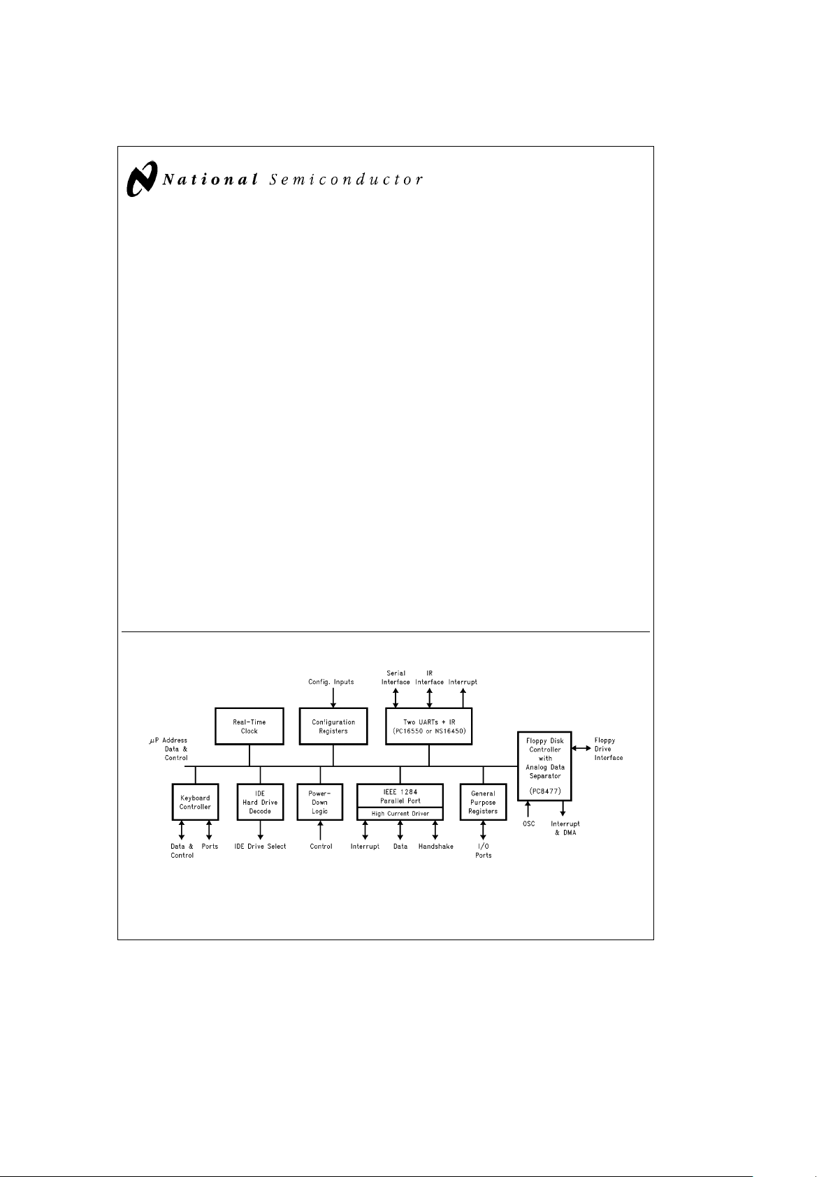
Block Diagram
TL/C/12379– 1
TRI-STATEÉis a registered trademark of National Semiconductor Corporation.
SuperI/O
TM
is a trademark of National Semiconductor Corporation.
MicroChannel
É
, PC-ATÉand PS/2Éare registered trademarks of International Business Machines Corporation.
C
1995 National Semiconductor Corporation RRD-B30M115/Printed in U. S. A.

General Description (Continued)
The RTC is a low-power design that provides a time-of-day
clock, a 100-year calendar, several alarm features and 242
bytes of general purpose RAM. An external battery is used
to maintain the time and contents of the general purpose
RAM, when power is removed from the PC87306. The
PC87306 RTC is compatible with the DS1287 and
MC146818 RTC devices.
The PC87306 FDC uses a high performance analog data
separator eliminating need for any external filter components. The FDC is fully compatible with the PC8477 and
incorporates a superset of DP8473, NEC mPD765 and
N82077 floppy disk controller function. All popular 5.25
×
and 3.5×floppy drives, including 2.88 MB 3.5×floppy drive,
are supported. Full TDR support for PC-AT and PS/2 floppy
drive types is also provided.
The two UARTs are fully NS16450 and NS16550 compatible.
The parallel port is fully IEEE 1284 level 2 compatible. The
SPP (Standard Parallel Port) is fully compatible with ISA,
EISA and MicroChannel parallel ports. In addition to the
SPP, EPP (Enhanced Parallel Port) and ECP (Extended Capabilities Port) modes are supported by the parallel port.
All IDE control signals with DMA support, including support
for Type F DMA are provided by the PC87306. Only external
signal buffers are required to implement a complete IDE
interface.
A set of fourteen configuration registers are provided to
control various functions of the PC87306. These registers
are accessed using two 8-bit wide index and data registers.
The ISA I/O address of the register pair can be relocated
using a power-up strapping option.
Two general purpose user programmable chip selects are
available. These chip selects can be used to decode game
port addresses.
Features (Continued)
Y
Real-Time Clock:
Ð DS1287, MC146818 and PC87911 compatible
Ð 242 Bytes battery backed-up CMOS RAM in two
banks
Ð Selective lock mechanism locks any half of the RTC
RAM
Ð Calendar in days, day of the week, months and
years with automatic leap-year adjustment
Ð Time of day in seconds, minutes and hours:
Ð12 or 24 hour format
Ð Optional daylight savings adjustment
Ð BCD or binary format for time keeping
Ð Three individually maskable interrupt event flags:
ÐPeriodic rates from 122 ms to 500 ms
ÐTime-of-day alarm once per second to once per
day
Ð Separate battery pin, 2.4V operation
Ð2mA typical power consumption
Ð Double buffer time registers
Y
UARTs:
Ð Software compatible with the PC16550A and
NS16450
Ð IrDA Infrared, and HP SIR Interface using UART2
with dedicated pins
Y
Parallel Port:
Ð EPP, ECP compatible with ECP level 2 support
Ð Bi-directional data transfer under software or
hardware control
Ð Includes protection circuit to prevent damage to the
parallel port when a connected printer is powered up
or is operated at a higher voltage
Y
IDE Control Logic:
Ð All IDE control signals, with DMA and support for
Type F DMA. Only external signal buffers are
required to implement the full IDE interface
Y
General Purpose Pins:
Ð Separate pins for two user programmable chip select
decoders provide ability to control a game port
Ð 16 additional general purpose I/O ports
Y
Address Decoder:
Ð Provides selection of all primary and secondary ISA
addresses including COM1– 4
Y
Plug and Play:
Ð Flexible IRQs and DMAs to meet the Plug and Play
requirements of Microsoft’s PC ’95 Hardware Design
Guide
Ð Multi-programmable parallel port base address
Y
General:
Ð ISA, EISA and MicroChannel compatible architecture
Ð Low power CMOS technology
Ð Ability to stop clocks to all modules
Ð The PC87323, which includes RAM KBC, can be
used as a development platform for KBC code for
the PC87306
Ð Reduced pin leakage current
Ð Special configuration register for power-down
Ð Disable bit for RTC
Ð 160-pin PQFP package
2

Table of Contents
1.0 PIN DESCRIPTION
2.0 CONFIGURATION REGISTERS
2.1 Overview
2.2 Software Configuration
2.3 Hardware Configuration
2.4 Index and Data Registers
2.5 Base Configuration Registers
2.5.1 Function Enable Register
2.5.2 Function Address Register
2.5.3 Power and Test Register
2.5.4 Function Control Register
2.5.5 Printer Control Register
2.5.6 KBC and RTC Control Register
2.5.7 Power Management Control Register
2.5.8 Tape, UARTs and Parallel Port Configuration
Register
2.5.9 SuperI/O Identification Register
2.5.10 Advanced SuperI/O Configuration Register
2.5.11 Chip Select 0 Low Address
2.5.12 Chip Select 0 High Address
2.5.13 Chip Select 0 Configuration Register
2.5.14 Chip Select 1 Low Address
2.5.15 Chip Select 1 High Address
2.5.16 Chip Select 1 Configuration Register
2.5.17 InfraRed Configuration Register
2.5.18 General Purpose I/O Port Base Address
Configuration Register
2.5.19 SuperI/O Configuration Register 0
2.5.20 SuperI/O Configuration Register 1
2.5.21 LPT Base Address Register
2.5.22 Plug and Play Configuration 0 Register
2.5.23 Plug and Play Configuration 1 Register
2.6 Power-Down Options
2.7 Power-Up Procedure and Considerations
2.7.1 UART Power-Up
2.7.2 FDC Power-Up
3.0 FDC REGISTER DESCRIPTION
3.1 FDC Control Registers
3.1.1 Status Register A (SRA) Read Only
3.1.2 Status Register B (SRB) Read Only
3.1.3 Digital Output Register (DOR) Read/Write
3.1.4 Tape Drive Register (TDR) Read/Write
3.1.5 Main Status Register (MSR) Read Only
3.1.6 Data Rate Select Register (DSR) Write Only
3.1.7 Data Register (FIFO) Read/Write
3.1.8 Digital Input Register (DIR) Read Only
3.1.9 Configuration Control Register (CCR)
Write Only
3.2 Result Phase Status Registers
3.2.1 Status Register 0 (ST0)
3.2.2 Status Register 1 (ST1)
3.0 FDC REGISTER DESCRIPTION (Continued)
3.2.3 Status Register 2 (ST2)
3.2.4 Status Register 3 (ST3)
4.0 FDC COMMAND SET DESCRIPTION
4.1 Command Descriptions
4.1.1 Configure Command
4.1.2 Dumpreg Command
4.1.3 Format Track Command
4.1.4 Invalid Command
4.1.5 Lock Command
4.1.6 Mode Command
4.1.7 NSC Command
4.1.8 Perpendicular Mode Command
4.1.9 Read Data Command
4.1.10 Read Deleted Data Command
4.1.11 Read ID Command
4.1.12 Read A Track Command
4.1.13 Recalibrate Command
4.1.14 Relative Seek Command
4.1.15 Scan Commands
4.1.16 Seek Command
4.1.17 Sense Drive Status Command
4.1.18 Sense Interrupt Command
4.1.19 Set Track Command
4.1.20 Specify Command
4.1.21 Verify Command
4.1.22 Version Command
4.1.23 Write Data Command
4.1.24 Write Deleted Data Command
4.2 Command Set Summary
4.3 Mnemonic Definitions for FDC Commands
5.0 FDC FUNCTIONAL DESCRIPTION
5.1 Microprocessor Interface
5.2 Modes of Operation
5.3 Controller Phases
5.3.1 Command Phase
5.3.2 Execution Phase
5.3.2.1 DMA ModeÐFIFO Disabled
5.3.2.2 DMA ModeÐFIFO Enabled
5.3.2.3 Interrupt ModeÐFIFO Disabled
5.3.2.4 Interrupt ModeÐFIFO Enabled
5.3.2.5 Software Polling
5.3.3 Result Phase
5.3.4 Idle Phase
5.3.5 Drive Polling Phase
5.4 Data Separator
5.5 Crystal Oscillator
5.6 Perpendicular Recording Mode
5.7 Data Rate Selection
5.8 Write Precompensation
3

Table of Contents (Continued)
5.0 FDC FUNCTIONAL DESCRIPTION (Continued)
5.9 FDC Low Power Mode Logic
5.10 Reset Operation
6.0 SERIAL PORTS
6.1 Serial Port Registers
6.2 Line Control Register (LCR) Read/Write
6.3 Programmable Baud Rate Generator
6.4 Line Status Register (LSR)
6.5 FIFO Control Register (FCR)
6.6 Interrupt Identification Register (IIR)
6.7 Interrupt Enable Register (IER)
6.8 MODEM Control Register (MCR)
6.9 MODEM Status Register (MSR)
6.10 Scratchpad Register (SCR)
7.0 SERIAL INFRARED WIRELESS COMMUNICATION
PORT
8.0 PARALLEL PORT
8.1 Introduction
8.2 Data Register (DTR)
8.3 Status Register (STR)
8.4 Control Register (CTR)
8.5 Enhanced Parallel Port Operation
8.6 Extended Capabilities Parallel Port (ECP)
8.6.1 Introduction
8.6.2 Software Operation
8.7 Register Definitions
8.8 Software Controlled Data Transfer
8.9 Automatic Data Transfer
8.9.1 Forward Direction
8.9.2 ECP Forward Write Cycle
8.9.3 Backward Direction
8.9.4 ECP Backward Read Cycle
8.10 FIFO Test Access
8.11 Configuration Registers Access
8.12 Interrupt Generation
9.0 INTEGRATED DEVICE ELECTRONICS INTERFACE
(IDE)
9.1 Introduction
9.2 IDE Signals
10.0 KEYBOARD CONTROLLER AND REAL-TIME
CLOCK
10.1 PC87306 KBC Function
10.1.1 Host System Interface
10.1.2 Program Memory
10.1.3 Data Memory and Registers
10.1.4 I/O Interface
10.1.5 Timer/Counter
10.0 KEYBOARD CONTROLLER AND REAL-TIME
CLOCK (Continued)
10.1.6 Interrupts
10.1.7 Oscillator and Instruction Timing
10.2 Real-Time Clock Function
10.2.1 Memory Map
10.2.2 Bus Interface
10.2.3 Time Generation
10.2.4 Time Keeping
10.2.5 RAM
10.2.6 Power Management
10.2.7 System Bus Lock Out and Power-Up
Detection
10.2.8 Oscillator
10.2.9 Interrupt Handling
10.2.10 Control Registers
11.0 GENERAL PURPOSE INPUT AND OUTPUT (GPIO)
PORTS
12.0 ELECTRICAL CHARACTERISTICS
12.1 DC Electrical Characteristics
12.1.1 Microprocessor, Parallel Port, and
IDE Interface Pins
12.1.2 Disk Interface Pins
12.1.3 Oscillator Pin
12.1.4 Parallel Port Pins
12.1.5 GPIO Pins
12.1.6 Keyboard Controller and Real-Time Clock
Pins
12.2 AC Electrical Characteristics
12.2.1 AC Test Conditions
12.2.2 Clock Timing
12.2.3 Microprocessor Interface Timing
12.2.4 Baud Out Timing
12.2.5 Transmitter Timing
12.2.6 Receiver Timing
12.2.7 MODEM Control Timing
12.2.8 DMA Timing
12.2.8.1 FDC
12.2.8.2 ECP
12.2.9 Reset Timing
12.2.10 FDC Write Data Timing
12.2.11 FDC Read Data Timing
12.2.12 Drive Control Timing
12.2.13 IDE Timing
12.2.14 Parallel Port Timing
12.2.15 Enhanced Parallel Port Timing
12.2.16 Extended Capabilities Port Timing
12.2.16.1 Forward
12.2.16.2 Backward
12.2.17 GPIO Write Timing
12.2.18 RTC
12.2.19 Programmable Chip Select Timing
4

List of Figures
FIGURE 1-1 Pins Which Utilize the Strap Function during Reset
FIGURE 1-2 Multi-Function Pins
FIGURE 2-1 PC87306 Configuration Registers
FIGURE 2-2 PC87306 Four Floppy Drive Circuit
FIGURE 3-1 FDC Functional Block Diagram
FIGURE 4-1 FDC Command Structure
FIGURE 4-2 IBM, Perpendicular, and ISO Formats Supported by the Format Command
FIGURE 5-1 FDC Data Separator Block Diagram
FIGURE 5-2 PC87306 Dynamic Window Margin Performance
FIGURE 5-3 Read Data AlgorithmÐState Diagram
FIGURE 5-4 Perpendicular Recording Drive R/W Head and Pre-Erase Head
FIGURE 6-1 PC87306 Composite Serial Data
FIGURE 6-2 Receiver FIFO Trigger Level
FIGURE 7-1 UART2 Serial and IR Interface Block Diagram
FIGURE 8-1 EPP 1.7 Address Write
FIGURE 8-2 EPP 1.7 Address Read
FIGURE 8-3 EPP Write with ZWS
FIGURE 8-4 EPP 1.9 Address Write
FIGURE 8-5 EPP 1.9 Address Read
FIGURE 8-6 ECP Forward Write Cycle
FIGURE 8-7 ECP Backward Read Cycle
FIGURE 9-1 IDE Interface Signal Equations (Non-DMA)
FIGURE 10-1 Keyboard Controller Functional Block Diagram
FIGURE 10-2 Keyboard Controller to Host System Interface
FIGURE 10-3 Status Register
FIGURE 10-4 Fast IRQ Latching and Clearing
FIGURE 10-5 Keyboard Controller Data Memory Map
FIGURE 10-7 PSW Register Bits
FIGURE 10-6 Keyboard Controller Stack Organization
FIGURE 10-8 Active Pull-Up I/O Port Structure
FIGURE 10-9 Using Port Pins as Inputs
FIGURE 10-10 Timing Generation and Timer Circuit
FIGURE 10-11 External Clock Connection
FIGURE 10-12 Instruction Cycle Timing
FIGURE 10-13 Oscillator Internal and External Circuitry
FIGURE 10-14 Interrupt/Status Timing
FIGURE 10-15 Typical Battery Configuration
FIGURE 10-16 Typical Battery Current during Battery Backed Mode
FIGURE 11-1 General Purpose I/O (GPIO) Ports
FIGURE 12-1 Clock Timing
FIGURE 12-2 Microprocessor Read Timing
FIGURE 12-3 Microprocessor Write Timing
FIGURE 12-4 Read after Write Operation to All Registers and RAM Timing
FIGURE 12-5 Baud Out Timing
FIGURE 12-6 Transmitter Timing
FIGURE 12-7 Receiver Timing
FIGURE 12-8 FIFO Mode Receiver Timing
FIGURE 12-9 Timeout Receiver Timing
FIGURE 12-10 MODEM Control Timing
FIGURE 12-11 FDC DMA Timing
FIGURE 12-12 ECP DMA Timing
FIGURE 12-13 Reset Timing
FIGURE 12-14 Write Data Timing
5

List of Figures (Continued)
FIGURE 12-15 Read Data Timing
FIGURE 12-16 Drive Control Timing
FIGURE 12-17 IDE Timing
FIGURE 12-18 Compatible Mode Parallel Port Interrupt Timing
FIGURE 12-19 Extended Mode Parallel Port Interrupt Timing
FIGURE 12-20 Typical Parallel Port Data Exchange
FIGURE 12-21 Enhanced Parallel Port Timing
FIGURE 12-22 ECP Parallel Port Forward Timing Diagram
FIGURE 12-23 ECP Parallel Port Backward Timing Diagram
FIGURE 12-24 GPIO Write Timing
FIGURE 12-25 IRQ
Release Delay
FIGURE 12-26 MR Timing
FIGURE 12-27 Chip Select Timing
List of Tables
TABLE 1-1 Pin Descriptions (Alphabetical)
TABLE 2-1 Default Configurations Controlled by Hardware on Reset
TABLE 2-2 Index and Data Register Optional Locations
TABLE 2-3 Encoded Drive and Motor Pin Information (FER 4
e
1)
TABLE 2-4 Primary and Secondary Drive Address Selection
TABLE 2-5 Parallel Port Addresses
TABLE 2-6 COM Port Selection for UART1
TABLE 2-7 COM Port Selection for UART2
TABLE 2-8 Address Selection for COM3 and COM4
TABLE 2-9 TRI-STATE Conditions of IRQ5 and IRQ7
TABLE 2-10 TRI-STATE Conditions of IRQ3 and IRQ4
TABLE 2-11 Parallel Port Mode
TABLE 3-1 Register Description and Addresses
TABLE 3-2 Drive Enable Values
TABLE 3-3 TDR Operation Modes
TABLE 3-4 Media ID Bits Functions
TABLE 3-5 Tape Drive Assignment Values
TABLE 3-6 Write Precompensation Delays
TABLE 3-7 Default Precompensation Delays
TABLE 3-8 Data Rate Select Encoding
TABLE 4-1 Typical Format GAP3 Length Values Based on Drive Data Rate
TABLE 4-2 Typical Format GAP3 Length Values Based on PC Compatible Diskette Media
TABLE 4-3 DENSEL Default Encoding
TABLE 4-4 DENSEL Encoding
TABLE 4-5 Head Settle Time Calculation
TABLE 4-6 Effect of Drive Mode and Data Rate on Format and Write Commands
TABLE 4-7 Effect of GAP and WG on Format and Write Commands
TABLE 4-8 Sector Size Selection
TABLE 4-9 SK Effect on the Read Data Command
TABLE 4-10 Result Phase Termination Values with No Error
TABLE 4-11 SK Effect on the Read Deleted Data Command
TABLE 4-12 Maximum Recalibrate
TABLE 4-13 Scan Command Termination Values
TABLE 4-14 Status Register 0 Termination Codes
TABLE 4-15 Set Track Register Address
TABLE 4-16 Step Rate Time (SRT) Values
TABLE 4-17 Motor Off Time (MFT) Values
6

List of Tables (Continued)
TABLE 4-18 Motor On Time (MNT) Values
TABLE 4-19 Verify Command Result Phase
TABLE 6-1 PC87306 UART
TABLE 6-2 PC87306 Register Summary for an Individual UART Channel
TABLE 6-3 PC87306 UART Reset Configuration
TABLE 6-4 PC87306 UART Divisors, Baud Rates and Clock Frequencies
TABLE 6-5 PC87306 Interrupt Control Functions
TABLE 8-1 Parallel Interface
TABLE 8-2 Standard Parallel Port
TABLE 8-3 SPP Data Register Read and Write Modes
TABLE 8-4 Parallel Port Reset States
TABLE 8-5 EPP Register Addresses
TABLE 8-6 Parallel Port Pin Out
TABLE 8-7 ECP Registers
TABLE 9-1 IDE Registers and Their ISA Addresses
TABLE 10-1 Summary of System Interface Operations
TABLE 10-2 RTC Memory Map
TABLE 12-1 Nominal t
ICP,tDRP
Values
TABLE 12-2 Minimum t
WDW
Values
7
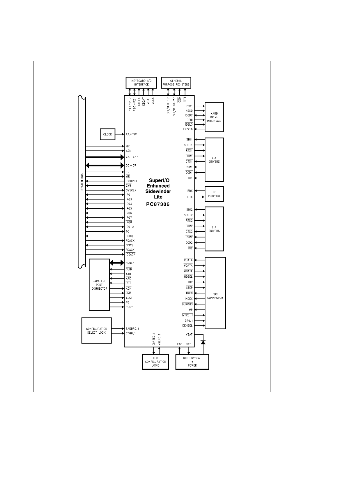
Basic Configuration
TL/C/12379– 2
8
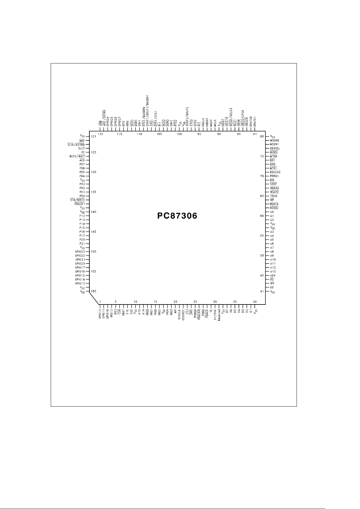
Connection Diagram
Plastic Quad Flatpak
TL/C/12379– 3
Note: Do not connect pins marked Reserved.
Order Number PC87306VUL
See NS Package Number VUL160A
9

1.0 Pin Description
TABLE 1-1. Pin Descriptions (Alphabetical)
Symbol Pin I/O Function
A0–A15 61–59, 56 – 46, I Address. These address lines from the microprocessor determine which internal register is
accessed. A0–A10 are don’t cares during an DMA transfer. A10 is used only during ECP
12–11
operations.
ACK 127 I Parallel Port Acknowledge. This input is pulsed low by a connected printer to indicate that it
has received data from the parallel port. This pin has a nominal 25 kX pull-up resistor
attached to it. (See DR1
and Table 7-5 for further information.)
AFD 119 I/O Parallel Port Automatic Feed. When this signal is low the printer should automatically line
feed after each line is printed. This pin is in a TRI-STATE
É
condition 10 ns aftera0isloaded
into the corresponding Control Register bit. The system should pull this pin high using a 4.7
kX resistor. (See DSTRB
and Table 8-5 for further information.)
AEN 45 I Address Enable. This input disables function selection via A15 – A0 when it is high. Access
during DMA transfer is NOT affected by this pin.
ASTRB 123 O Address Strobe. This signal is used in Enhanced Parallel Port (EPP) mode as an address
strobe. It is active low. (See SLIN and Table 8-5 for further information.)
BADDR0,1 109, 108 I Base Address. These CMOS inputs are sensed during reset to determine one of four base
addresses from which the Index and Data Registers are offset (see Table 2-2). An internal
pull-down resistor of 30 kX is present on this pin. Use a 10 kX resistor to pull this pin to V
DD
.
(See RTS1
, SOUT1, and BOUT1 for further information.)
BOUT1,2 108, 98 O BAUD Output. This multi-function pin provides the associated serial channel Baud Rate
generator output signal when test mode is selected in the Power and Test Configuration
Register and the DLAB bit (LCR7) is set. After a Master Reset, this pin provides the Serial
Output (SOUT) function. (See SOUT and BADDR1 for further information.)
BUSY 126 I Parallel Port Busy. This pin is set high by a connected printer when it cannot accept another
character. It has a nominal 25 kX pull-down resistor attached to it. (See WAIT
and Table 8-5
for further information.)
CFG0, 1 84, 106 I Configuration on Power-Up. These CMOS inputs select 1 of 4 default configurations in
which the PC87306 powers-up (see Table 2-1). They are provided with CMOS input buffers.
An internal pull-down resistor of 30 kX is present on each pin. Use a 10 kX resistor to pull
these pins to VDD.
CS0, 1 6, 23 O Programmable Chip Select. CS0, 1 are programmable chip select and/or latch enable and/
or output enable signals that can be used for a game port, I/O port expander or other add-on
peripheral. The decoded address and the assertion conditions are configured via the
PC87306 configuration registers, 0Ah–0Dh and 10h – 11h.
CTS1,2 107, 97 I Clear to Send. When low, this indicates that the MODEM or data set is ready to exchange
data. The CTS
signal is a MODEM status input whose condition the CPU can test by reading
bit 4 (CTS) of the MODEM Status Register (MSR) for the appropriate serial channel. Bit 4 is
the complement of the CTS
signal. Bit 0 (DCTS) of the MSR indicates whether the CTS input
has changed state since the previous reading of the MSR. CTS
has no effect on the
transmitter.
Note: Whenever the DCTS bit of the MSR is set an interrupt is generated if MODEM Status interrupts are enabled.
D7–0 33 – 39, 42 I/O Data. Bi-directional data lines to the microprocessor. D0 is the LSB and D7 is the MSB.
These signals all have 24 mA (sink) buffered outputs.
DCD1,2 112, 104 I UARTs Data Carrier Detect. When low, this signal indicates that the MODEM or data set
has detected the data carrier. The DCD signal is a MODEM status input whose condition the
CPU can test by reading bit 7 (DCD) of the MODEM Status Register (MSR) for the
appropriate serial channel. Bit 7 is the complement of the DCD
signal. Bit 3 (DDCD) of the
MSR indicates whether the DCD
input has changed state since the previous reading of the
MSR.
Note: Whenever the DDCD bit of the MSR is set, an interrupt is generated if MODEM Status interrupts are enabled.
DENSEL 77 O FDC Density Select. Indicates that a high FDC density data rate (500 kbps or 1 Mbps) or a
low density data rate (250 kbps or 300 kbps) is selected. DENSEL’s polarity is controlled by
bit 6 of the ASC register.
10

1.0 Pin Description (Continued)
TABLE 1-1. Pin Descriptions (Alphabetical) (Continued)
Symbol Pin I/O Function
DIR 69 O FDC Direction. This output determines the direction of the floppy disk drive (FDD) head
movement (active
e
step in, inactiveestep out) during a seek operation. During reads or writes,
DIR is inactive.
DR0, 1 73, 74 O FDC Drive Select 0, 1. These are the decoded Drive Select outputs that are controlled by the
Digital Output Register bits D0, D1. The Drive Select outputs are gated with DOR bits 4–7. These
are active low outputs. They are encoded with information to control four FDDs when bit 4 of the
Function Enable Register (FER) is set. (See MTR0, 1 for more information.)
DRATE0, 1 82, 81 O FDC Data Rate 0, 1. These outputs reflect the currently selected FDC data rate (bits 0 and 1 in
the Configuration Control Register (CCR) or the Data Rate Select Register (DSR), whichever was
written to last). These pins are totem-pole buffered outputs (6 mA sink, 6 mA source).
DSKCHG 71 I FDC Disk Change. This input indicates if the drive door has been opened. The state of this pin is
available from the Digital Input register. This pin can also be configured as the Read Gate
(RGATE) data separator diagnostic input via the Mode command (see Section 4.2.6).
DSR1, 2 111, 103 I UARTs Data Set Ready. When low, this signal indicates that the data set or MODEM is ready to
establish a communications link. The DSR
signal is a MODEM status input whose condition the
CPU can test by reading bit 5 (DSR) of the MODEM Status Register (MSR) for the appropriate
channel. Bit 5 is the complement of the DSR
signal. Bit 1 (DDSR) of the MSR indicates whether
the DSR
input has changed state since the previous reading of the MSR.
Note: Whenever the DDSR bit of the MSR is set, an interrupt is generated if MODEM Status interrupts are enabled.
DSTRB 119 O Data Strobe. This signal is used in EPP mode as a data strobe. It is active low. (See AFD and
Table 8-5 for further information.)
DTR1, 2 106, 96 O UARTs Data Terminal Ready. When low, this output indicates to the MODEM or data set that
the UART is ready to establish a communications link. The DTR
signal can be set to an active low
by programming bit 0 (DTR) of the MODEM Control Register to a high level. A Master Reset
operation sets this signal to its inactive (high) state. Loop mode operation holds this signal to its
inactive state. (See CFG0, 1 for further information.)
ERR 120 I Error. A connected printer sets this input low when it has detected an error. This pin has a
nominal 25 kX pull-up resistor attached to it.
FDACK 28 I FDC DMA Acknowledge. Active low input to acknowledge the FDC DMA request and enable the
RD
and WR inputs during a DMA transfer. When in PC-AT or Model 30 mode, this signal is
enabled by bit D3 of the Digital Output Register (DOR). When in PS/2 mode, FDACK
is always
enabled, and bit D3 of the DOR is reserved. FDACK
should be held high during I/O accesses.
FDRQ 27 O DMA Request. Active high output to signal the DMA controller that a FDC data transfer is
needed. When in PC-AT or Model 30 mode, this signal is enabled by bit D3 of the DOR. When in
PS/2 mode, FDRQ is always enabled, and bit D3 of the DOR is reserved.
GPIO10–17 3-1, I/O General Purpose I/O10 – 17. General purpose I/O pins of I/O port 1.
158–154
GPIO20–27 153 –150, I/O General Purpose I/O20 – 27. General purpose I/O pins of I/O port 2.
118–115
HCS0 87 O Hard Drive Chip Select 0. This output is active in the PC-AT mode when 1) the hard drive
registers from 1F0–1F7h are selected and the primary address is used or 2) when the hard drive
registers from 170–177h are selected and the secondary address is used. This output is inactive
if the IDE interface is disabled via the Configuration Register. HCS0
is multiplexed with SELCS
strap input. A 40 kX internal pull-up resistor is, therefore, used on this pin during reset. (See
SELCS for further information.)
HCS1 86 O Hard Drive Chip Select 1. This output is active in the PC-AT mode when 1) the hard drive
registers from 3F6–7 are selected and the primary address is used or 2) the hard drive registers
from 376–377 are selected and the secondary address is used. This output is also inactive, if the
IDE interface is disabled via the Configuration Register.
11
1.0 Pin Description (Continued)
TABLE 1-1. Pin Descriptions (Alphabetical) (Continued)
Symbol Pin I/O Function
HDSEL 62 O FDC Head Select. This output determines which side of the FDD is accessed. When Active, the head
selects side 1. When inactive, the head selects side 0.
IDEACK 83 I IDE DMA Acknowledge. This is the IDE DMA acknowledge input pin when bit 1 of FCR is 1.
IDED7 89 I/O IDE Bit 7. This pin provides the data bus bit 7 signal to the IDE hard drive during accesses in the
address range 1F0–1F7h, 170 – 177h, 3F6h and 376h. This pin is TRI-STATE during read or write
accesses to 3F7h and 377h.
IDEHI 85 O IDE High Byte. This output enables the high byte data latch during a read or write to the hard drive if
the hard drive returns IOCS16
. This output is inactive if the IDE interface is disabled via the
Configuration Register.
IDELO 84 O IDE Low Byte. This output enables the low byte data latch during a read or write to the hard drive. This
output is inactive if the IDE interface is disabled via the Configuration Register. (See CFG0 for further
information.)
INDEX 76 I FDC Index. This input signals the beginning of a FDD track.
INIT 122 I/O Initialize. When this signal is low it causes a connected printer to be initialized. This pin is in a TRI-
STATE condition 10 ns aftera1isloaded into the corresponding Control Register bit. The system
should pull this pin high using a 4.7 kX resistor.
IOCHRDY 22 O I/O Channel Ready. This is the I/O Channel Ready open drain output. When IOCHRDY is driven low,
the EPP extends the host cycle.
IOCS16 88 I I/O Chip Select 16-Bit. This input is driven by a connected peripheral device which can accommodate
a 16-bit access. This pin is configured when bit 2 of ASC is 0.
IRRX 113 I Infrared Receiver.
IRTX 114 O Infrared Transmitter.
IRQ1 5 I/O Interrupt 1. KBC’s keyboard interrupt generated from internal P24 of the KBC.
IRQ3, 4 19, 18 O Interrupt 3 and 4. These are active high interrupts associated with the serial ports. When bit 0 of the
Plug and Play register (PNP1) is 0, IRQ3 presents the signal if the serial channel has been designated
as COM2 or COM4 and IRQ4 presents the signal if the serial port is designated as COM1 or COM3.
The appropriate interrupt goes active whenever it is enabled via the Interrupt Enable Register (IER),
the associated Interrupt Enable bit (Modem Control Register bit 3, MCR3), and any of the following
conditions are active: Receiver Error, Receive Data available, Transmitter Holding Register Empty, or a
Modem Status Flag is set. The interrupt signal is reset low (inactive) after the appropriate interrupt
service routine is executed, after being disabled via the IER, or after a Master Reset.
Either interrupt can be disabled, putting it into TRI-STATE, by setting the MCR3 bit low. When bit 0 of
the PNP1 register is 1, IRQ3 and IRQ4 are selected according to bits 2 amd 6 of the PNP1 register.
See Table 2-10 for IRQ3 and IRQ4 TRI-STATE conditions.
IRQ5 16 I/O Interrupt 5. Active high output that indicates a parallel port interrupt. When enabled this bit follows the
ACK
signal input. When bit 4 in the parallel port Control Register is set and the parallel port address is
designated as shown in Table 2-5, this interrupt is enabled. When it is not enabled this signal is
TRI-STATE.
This pin is I/O only when ECP is enabled, IRQ5 is configured, and bit 6 of PCR is 1. When bit 4 of the
PNP0 register is 1, IRQ5 and IRQ7 are selected according to bit 5 of the PNP0 register. See Table 2-9
for IRQ5 and IRQ7 TRI-STATE conditions.
IRQ6 15 O Interrupt 6. Active high output to signal the completion of the execution phase for certain FDC
commands. Also used to signal when a data transfer is ready during a Non-DMA operation. When in
PC-AT or Model 30 mode, this signal is enabled by bit D3 of the DOR. When in PS/2 mode, IRQ6 is
always enabled, and bit D3 of the DOR is reserved.
IRQ7 14 I/O Interrupt 7. Active high output that indicates a parallel port interrupt. When enabled this bit follows the
ACK
signal input. When bit 4 in the parallel port Control Register is set and the parallel port address is
designated as shown in Table 2-5, this interrupt is enabled. When it is not enabled this signal is
TRI-STATE.
This pin is I/O only when ECP is enabled, IRQ7 is configured, and bit 6 of PCR is 1. For ECP operation,
refer to the interrupt ECP Section 7.11.1
12

1.0 Pin Description (Continued)
TABLE 1-1. Pin Descriptions (Alphabetical) (Continued)
Symbol Pin I/O Function
IRQ8 13 O Interrupt 8. Real-Time Clock interrupt request output. This is an open-drain output.
IRQ12 4 I/O Interrupt 12. KBC’s mouse interrupt generated from internal P25 of the KBC.
KBCLK 94 I/O Keyboard Clock output. Connected internally to KBC’s T0.
KBDAT 93 I/O Keyboard Data output. Connected internally to KBC’s P10.
MCLK 91 I/O Mouse Clock output. Connected internally to KBC’s T1.
MDAT 92 I/O Mouse Data output. Connected internally to KBC’s P11.
MR 20 I Master Reset. Active high input that resets the controller to the idle state, and resets all disk
interface outputs to their inactive states. The DOR, DSR, CCR, Mode command, Configure
command, and Lock command parameters are cleared to their default values. The Specify
command parameters are not affected. The Configuration Registers are set to their selected
default values.
MSEN0,1 79, 78 I Media Sense. These pins are Media Sense input pins when bit 0 of FCR is 0. Each pin has a
40 kX internal pull-up resistor.
MTR0, 1 75, 72 O FDC Motor Select 0, 1. These are the motor enable lines for drives 0 and 1, and are controlled by
bits D7–D4 of the Digital Output register. They are active low outputs. They are encoded with
information to control four FDDs when bit 4 of the Function Enable Register (FER) is set. MTR0
exchanges logical motor values with MTR1 when bit 4 of FCR is set. (See DR0,1.)
P12–P17 141 – 146 I/O KBC I/O Port. Quasi-bidirectional port for general purpose input and output.
P20, 21 147, 148 I/O KBC I/O Port. Open-drain port for general purpose input and output.
PD0–7 136 – 133, I/O Parallel Port Data. These bidirectional pins transfer data to and from the peripheral data bus and
the parallel port Data Register. These pins have high current drive capability. (See DC Electrical
131–128
Characteristics.)
PDACK0, 1 26, 138 I Parallel Port DMA Acknowledge. Active low input to acknowledge a connected printer’s DMA
request, and enable the RD
and WR inputs during a DMA transfer. These inputs are valid only in
Enhanced Capabilities Port (ECP) mode. At any given moment, one of these two pins is
connected. The pin which is not selected is ignored. See bit 3 of SCF1 for pin selection.
PDRQ0, 1 25, 70 O Parallel Port DMA Request. Active high output which signals the DMA controller that a printer
data transfer is required. These outputs are valid only in ECP mode. These pins are in TRI-STATE
when not selected. At any given moment, one of these two pins is connected. See bit 3 of SCF1
for pin selection.
PE 125 I Parallel Port Paper End. This input is set high by a connected printer which is out of paper. This
pin has a nominal 25 kX pull-down resistor attached to it.
RD 44 I Read. Active low input to signal a data read by the microprocessor.
RDATA 63 I FDC Read Data. This input is the raw serial data read from the floppy disk drive.
RI1, 2 105, 95 I Ring Indicator. When low this indicates that a telephone ring signal has been received by the
MODEM. The RI signal is a MODEM status input whose condition the CPU can test by reading bit
6 (RI) of the MODEM Status Register (MSR) for the appropriate serial channel. Bit 6 is the
complement of the RI signal. Bit 2 (TERI) of the MSR indicates whether the RI input has changed
from low to high since the previous reading of the MSR.
Note: When the TERI bit of the MSR is set, an interrupt is generated if MODEM Status interrupts are enabled.
RTS1, 2 109, 101 O Request to Send. When low, this output indicates to the MODEM or data set that the UART is
ready to exchange data. The RTS
signal can be set to an active low by programming bit 1 (RTS)
of the MODEM Control Register to a high level. A Master Reset operation sets this signal to its
inactive (high) state. Loop mode operation holds this signal to its inactive state. (See BADDR0 for
further information.)
SELCS 87 I National Strap Pin. A40kXinternal pull-up resistor. Do not pull this pin low during reset. (See
CS0CF bit 7.)
13
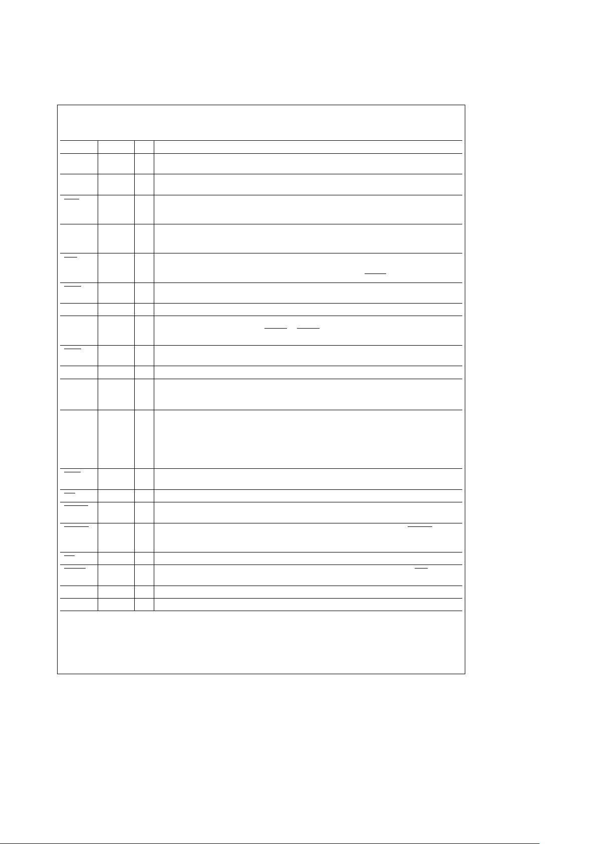
1.0 Pin Description (Continued)
TABLE 1-1. Pin Descriptions (Alphabetical) (Continued)
Symbol Pin I/O Function
SIN1, 2 110, 102 I Serial Input. This input receives composite serial data from the communications link (e.g. peripheral
device, MODEM, or data set).
SLCT 124 I Select. When a printer is connected, it sets this input high. This pin has a nominal 25 kX pull-down
resistor attached to it.
SLIN 123 I/O Select Input. When this signal is low it selects the printer. This pin is a TRI-STATE condition 10 ns
aftera0isloaded into the corresponding Control Register bit. The system should pull this pin high
using a 4.7 kX resistor.
SOUT1, 2 108, 98 O Serial Output. This output sends composite serial data to the communications link (peripheral
device, MODEM, or data set). The SOUT signal is set to a marking state (logic 1) after a Master
Reset operation. (See BOUT and BADDR1 for further information.)
STB 137 I/O Data Strobe. This output indicates to the printer that valid data is available at the printer port. This
pin is in a TRI-STATE condition 10 ns after a zero is loaded into the corresponding Control Register
bit. The system should pull this pin high using a 4.7 kX resistor. (See WRITE
for further information.)
STEP 68 O Step. This output signal issues pulses to the disk drive at a software programmable rate to move
the head during a seek operation.
SYSCLK 21 I System Clock. This input is used as the KBC input clock when bit 7 of KRR is 1.
TC 29 I Terminal Count. Control signal from the DMA controller to indicate the termination of a DMA
transfer. TC is accepted only when FDACK
or PDACK is active. TC is active high in PC-AT mode
and active low in PS/2 mode.
TRK0 65 I Track 0. This input indicates to the controller that the head of the selected floppy disk drive is at
track zero.
VBAT 7 Battery. Real-Time Clock battery pin.
VDD 160, 140, Digital Supply. This is the 5V supply voltage for the digital circuitry.
99, 57,
41, 17
VSS 159, 149, Digital Ground. This is the ground for the digital circuitry.
139, 132,
121, 100,
90, 80,
58, 40,
32, 10
WAIT 126 I Wait. This signal is used, in EPP mode, by the parallel port device to extend its access cycle. It is
active low. (See BUSY and Table 8-5 for further information.)
WR 43 I Write. Active low input to signal to indicate a write from the microprocessor to the controller.
WDATA 67 O Write Data. This output is the write precompensated serial data that is written to the selected floppy
disk drive. Precompensation is software selectable.
WGATE 66 O Write Gate. This output signal enables the write circuitry of the selected disk drive. WGATE has
been designed to prevent glitches during power up and power-down. This prevents writing to the
disk when power is cycled.
WP 64 I Write Protect. This input indicates that the floppy disk in the selected drive is write protected.
WRITE 137 O Write Strobe. This signal is used in EPP mode as a write strobe. It is active low. (See STB and
Table 8-5 for further information.)
X1 30 I Clock Oscillator. A TTL or CMOS compatible 24 MHz clock is connected to this pin.
X1C 8 I Crystal1 Slow. Input for the internal Real-Time Clock crystal oscillator amplifier.
14
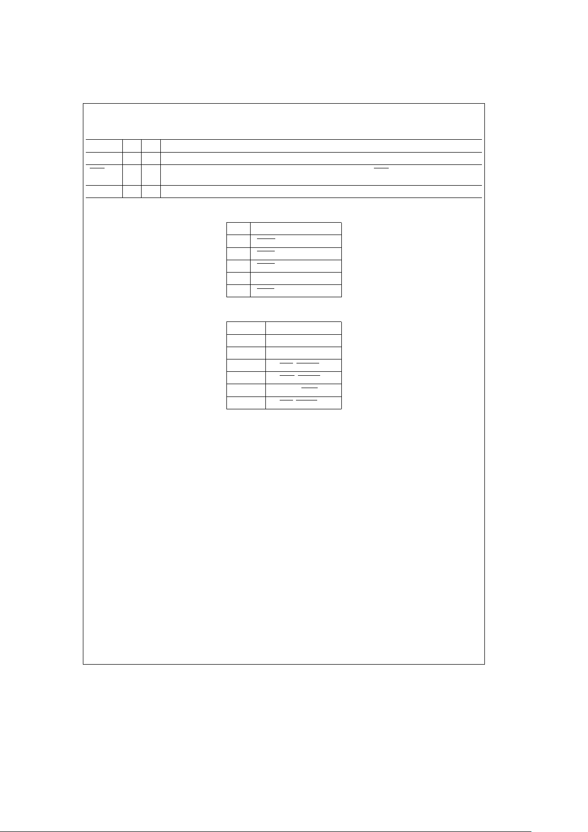
1.0 Pin Description (Continued)
TABLE 1-1. Pin Descriptions (Alphabetical) (Continued)
Symbol Pin I/O Function
X2C 9 O Crystal2 Slow. Output for the internal Real-Time Clock crystal oscillator amplifier.
ZWS 24 O Zero Wait State. This pin is the Zero Wait State open drain output pin. ZWS is driven low when the EPP,
or the ECP, is written, and the access can be shortened.
Reserved 31 Reserved. This pin must be left unconnected.
FIGURE 1-1. Pins Which Utilize the Strap Function During Reset
Pin Symbols
84 IDEL0/CFG0
87 HCS0/SELCS
106 DTR1/CFG1
108 SOUT1/BOUT1/BADDR1
109 RTS1/BADDR0
FIGURE 1-2. Multi-Function Pins
Pin Symbols
98 SOUT2/BOUT2
108 SOUT1/BOUT1
119 AFD/DSTRB
123 SLIN/ASTRB
126 BUSY/WAIT
137 STB/WRITE
15

2.0 Configuration Registers
2.1 OVERVIEW
Eighteen registers constitute the Base Configuration Register set, and control the PC87306 setup. In general, these
registers control the enabling of major functions (FDC,
UARTs, parallel port, pin functionalty etc.), the I/O addresses of these functions, and whether they power-down via
hardware control or not. These registers are the Function
Enable Register (FER), the Function Address Register
(FAR), the Power and Test Register (PTR), the Function
Control Register (FCR), the Printer Control Register (PCR),
the Keyboard and Real-Time Clock Control Register (KRR),
the Power Management Control Register (PMC), the Tape,
UARTs and Parallel Port Register (TUP), the SuperI/O Identification Register (SID), the Advanced SIO Configuration
Register (ASC), the Chip Select 0 Address Low Register
(CS0LA), the Chip Select 0 High Address Register (CS0HA),
the Chip Select 0 Configuraton Register (CS0CF), the Chip
Select 1 Low Address Register (CS1LA), the Chip Select 1
High Address Register (CS1HA), the Chip Select 1 Configuration Register (CS1CF), the Infrared Configuration Register
(IRC), the General Purpose I/O Port Base Address Configuration Register (GPBA), and the SuperI/O Configuration
Register 0 (SCF0).
The FER, FAR, PTR, KRR, and SCF0 registers can be accessed via hardware or software. During reset, the PC87306
loads a set of default values, selected by a hardware strapping option, into the FER, FAR, and PTR Configuration Registers. The remaining 13 registers can only be accessed by
software.
An index and data register pair are used to read and write
these registers. Each Configuration Register is pointed to by
the value loaded into the Index Register. The data to be
written into the Configuration Register is transferred via the
Data register. A Configuration Register is read in a similar
way (i.e., by pointing to it via the Index Register and then
reading its contents via the Data Register).
Accessing the Configuration Registers in this way requires
only two system I/O addresses. Since that I/O space is
shared by other devices the Index and Data Registers can
still be inadvertantly accessed. To reduce the chances of an
inadvertant access, a simple procedure (see Section 2.2)
has been developed.
To maintain compatibility with other SuperI/O chips, register
bits with reserved values may not be altered. Use a readmodify-write procedure.
2.2 SOFTWARE CONFIGURATION
If the system requires access to the Configuration Registers
after reset, the following procedure must be used to change
data in the registers.
1. Determine the PC87306 Index Register’s default location.
Check the four possible locations (see Table 2-1) by
reading them twice. The first byte is the ID byte 88h. The
second byte read is always 00h, but read after write always brings the value of the written byte. Compare the
data read with the ID byte and then 00h. A match occurs
at the correct location. Note that the ID byte is only issued from the Index Register during the first read after a
reset. Subsequent reads return the value loaded into the
Index Register. Bits 5 – 7 are reserved and always read 0.
2. Load the Configuration Registers.
A. Disable CPU interrupts.
B. Write the index of the Configuration Register (00h –
0Dh) to the Index Register one time.
C. Write the correct data for the Configuration Register in
two consecutive write accesses to the Data Register.
D. Enable CPU interrupts.
3. Load the Configuration Registers (read-modify-write).
A. Disable CPU interrupts.
B. Write the index of the Configuration Register (00h –
0Dh) to the Index Register one time.
C. Read the configuration data in that register via the
Data Register.
D. Modify the configuration data.
E. Write the changed data for the Configuration Register
in two consecutive writes to the Data Register. The
register updates on the second consecutive write.
F. Enable CPU interrupts.
A single read access to the Index and Data Registers can
be done at any time without disabling CPU interrupts. When
the Index Register is read, the last value loaded into the
Index Register is returned. When the Data Register is read,
the Configuration Register data pointed to by the Index Register is returned.
16
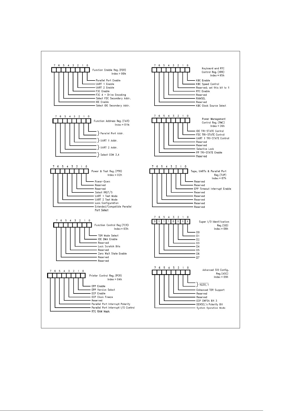
2.0 Configuration Registers (Continued)
TL/C/12379– 4
TL/C/12379– 6
TL/C/12379– 8
TL/C/12379– 10
TL/C/12379– 12
TL/C/12379– 5
TL/C/12379– 7
TL/C/12379– 9
TL/C/12379– 11
TL/C/12379– 13
FIGURE 2-1. PC87306 Configuration Registers
17
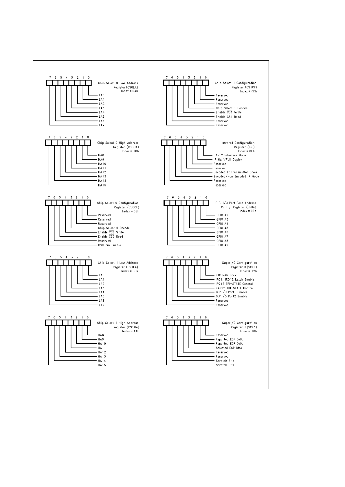
2.0 Configuration Registers (Continued)
TL/C/12379– 14
TL/C/12379– 15
TL/C/12379– 16
TL/C/12379– 17
TL/C/12379– 18
TL/C/12379– 19
TL/C/12379– 20
TL/C/12379– 21
TL/C/12379– 22
TL/C/12379– 97
FIGURE 2-1. PC87306 Configuration Registers (Continued)
18
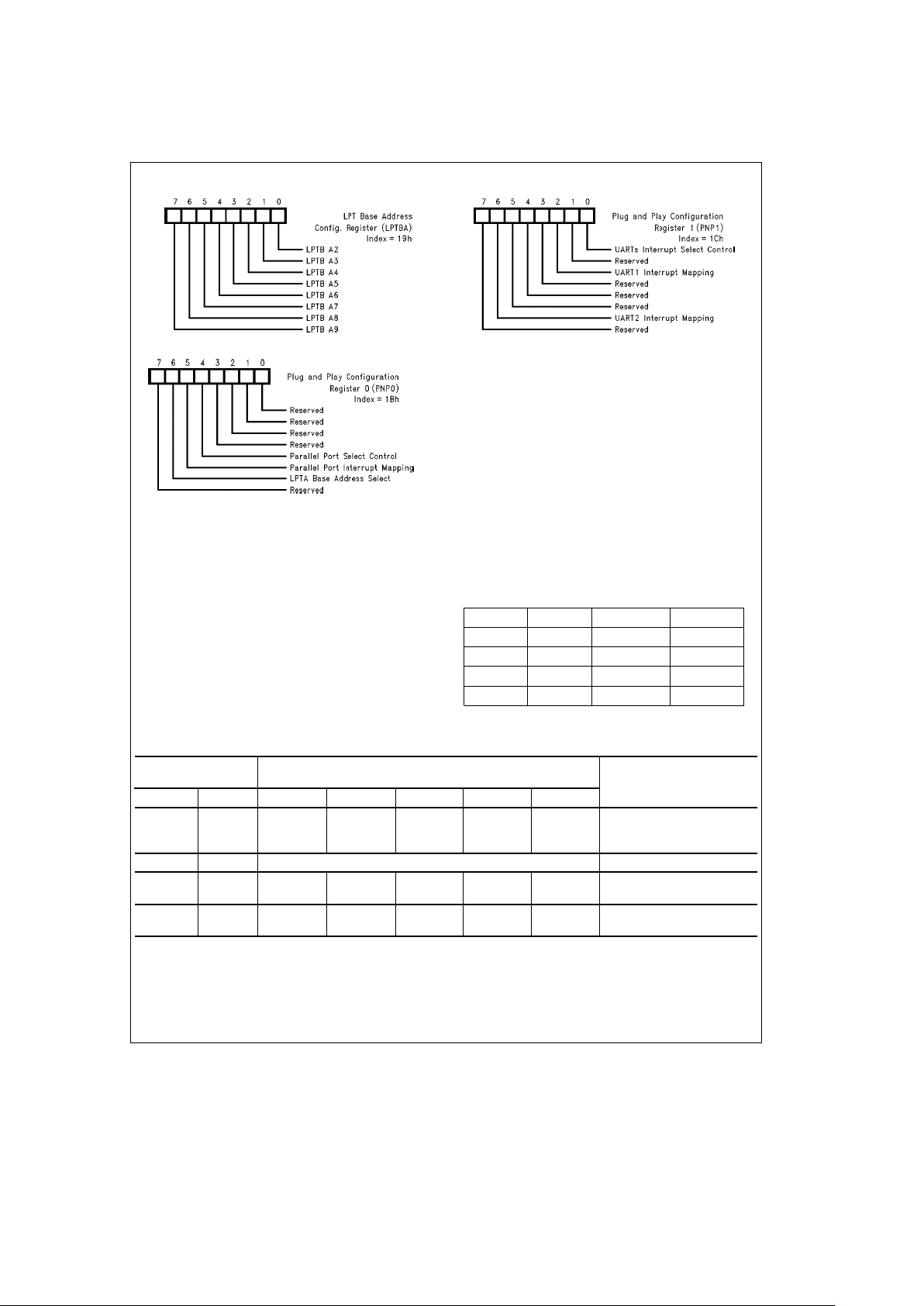
2.0 Configuration Registers (Continued)
TL/C/12379– 23 TL/C/12379– 25
TL/C/12379– 24
FIGURE 2-1. PC87306 Configuration Registers (Continued)
2.3 HARDWARE CONFIGURATION
During reset, 1 of 4 possible sets of default values are loaded into the first five Configuration Registers. A strapping
option on two pins (CFG0, 1) selects the set of values that is
loaded. This allows for automatic configuration without software intervention. Table 2-1 shows the 4 possible default
configurations. The default configuration can be modified by
software at any time after reset by using the access procedure described in the Software Configuration Section.
2.4 INDEX AND DATA REGISTERS
Another general aspect of the Configuration Registers is
that the Index and the Data Register pair can be relocated
to any one of two locations. This is controlled through a
hardware strapping option on two pins (BADDR0,1) and it
allows the registers to avoid conflicts with other adapters in
the I/O address space. Table 2-2 shows the address options.
TABLE 2-2. Index and Data Register
Optional Locations
BADDR1 BADDR0 Index Addr. Data Addr.
0 0 398 399
0 1 26E 26F
1 0 15C 15D
1 1 2E 2F
TABLE 2-1. Default Configurations Controlled by Hardware on Reset
Configuration
Configuration Register Reset Values (Binary)
Activated Functions
on Reset
Pins
CFG1 CFG0 FER FAR PTR KRR SCF0
0 0 01001011 00000001 00000x00 0x001101 0x110000 PRI (FDC), PRI (IDE),
LPTA, COM1, GPIO
KBC, RTC
0 1 Reserved Mode Reserved Mode
1 0 00001111 00010001 00000x00 0x001101 0x000000 PRI (FDC), LPTA, COM1,
COM2 (non-IR), KBC, RTC
1 1 00000000 00010000 00000x00 0x000001 0x000000 All Modules Disabled
(powered-down), except KBC
Where:
PRI is the PRImary floppy or IDE address; 3F0–7h or
1F0–7, 3F6, 3F7h)
COM1 is the UART address at 3F8–3FFh
COM2 is the UART address at 2F8–2FFh
LPTA is the Parallel Port address at 3BC – 3BEh
GPIO is the General Purpose I/O ports 1 and 2 addresses
at 78h and 79h
KBC is the Keyboard Controller function, using an
X1
d
3 clock
RTC is the Real-Time Clock function
19
2.0 Configuration Registers (Continued)
2.5 BASE CONFIGURATION REGISTERS
2.5.1 Function Enable Register (FER, Index 00h)
This register enables and disables major chip functions. Disabled functions have their clocks automatically powered
down, but the data in their registers remains intact. It also
selects whether the FDC and the IDE controller is located at
their primary or secondary address. See Table 2-1 for the
FER reset value.
Bit 0 When this bit is one the parallel port can be accessed
at the address specified in the FAR.
Bit 1 When this bit is one, UART1 can be accessed at the
address specified in the FAR. When this bit is zero,
access to UART1 is blocked and it is in power-down
mode. The UART1 registers retain all data in power
down mode.
Caution: Any UART1 interrupt that is enabled and
active or becomes active after UART1 is disabled asserts the associated IRQ pin when UART1 is disabled. If disabling UART1 via software, clear the IRQ
Enable bit (MCR3) to zero before clearing FER 1.
This is not an issue after reset because MCR3 is zero
until it is written.
Bit 2 When this bit is one, UART2 can be accessed at the
address specified in the FAR. When this bit is zero,
access to UART2 is blocked and it is in power-down
mode. The UART2 registers retain all data in power
down mode.
Caution: Any UART2 interrupt that is enabled and
active or becomes active after UART2 is disabled asserts the associated IRQ pin when UART1 is disabled
If disabling UART2 via software, clear the IRQ Enable bit (MCR3) to zero before clearing FER1. This is
not an issue after reset because MCR3 is zero until it
is written.
Bit 3 When this bit is one, the FDC can be accessed at the
address specified in the FER bits. When this bit is
zero access to the FDC is blocked and it is in powerdown mode. The FDC registers retain all data in power down mode.
Bit 4 When this bit is zero the PC87306 can control two
floppy disk drives directly without an external decoder. When this bit is one the two drive select signals
and two motor enable signals from the FDC are encoded so that four floppy disk drives can be controlled (see Table 2-3 and
Figure 2-2
). Controlling
four FDDs requires an external decoder. The pin
states shown in Table 2-3 are a direct result of the bit
patterns shown. All other bit patterns produce pin
states that should not be decoded to enable any
drive or motor.
Bit 5 This bit selects the primary or secondary FDC ad-
dress. (See Table 2-4.)
Bit 6 When this bit is a one the IDE drive interface can be
accessed at the address specified by FER bit 7.
When it is zero, bit 0 of PMC determines whether the
HCS0,1
pins are inactive, or in TRI-STATE. IDEHI
and IDEHLO are inactive and IDED7 is in TRISTATE.
Bit 7 This bit selects the primary or secondary IDE ad-
dress. (See Table 2-4).
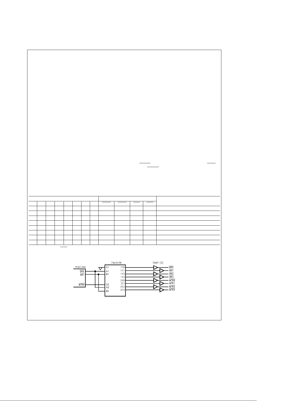
TABLE 2-3. Encoded Drive and Motor Pin Information (FER 4
e
1)
Digital Output Register Drive Control Pins
Decoded Functions
7 6 5 4 3 2 1 0 MTR1 MTR0 DR1 DR0
XXX1X X 0 0 (Note) 0 0 0 Activate Drive 0 and Motor 0
XX1X X X 0 1 (Note) 0 0 1 Activate Drive 1 and Motor 1
X 1 X X X X 1 0 (Note) 0 1 0 Activate Drive 2 and Motor 2
1 X X X X X 1 1 (Note) 0 1 1 Activate Drive 3 and Motor 3
XXX0X X 0 0 (Note) 1 0 0 Activate Drive 0 and Deactivate Motor 0
XX0X X X 0 1 (Note) 1 0 1 Activate Drive 1 and Deactivate Motor 1
X 0 X X X X 1 0 (Note) 1 1 0 Activate Drive 2 and Deactivate Motor 2
0 X X X X X 1 1 (Note) 1 1 1 Activate Drive 3 and Deactivate Motor 3
Note: When FER4e1, MTR1 presents a pulse that is the inverted image of the IOW strobe. This inverted pulse is active whenever an I/O write to address 3F2h or
372h takes place. This pulse is delayed by 25 ns– 80 ns after the leading edge of IOW and its leading edge can be used to clock data into an external latch (e.g.,
74LS175). Address 3F2h is used if the FDC is located at the primary address (FER5
e
0) and address 372h is used if the FDC is located at the secondary address
(FER5
e
1).
TL/C/12379– 26
Hex Buffers
I
CC
e
40 mA
open collector
FIGURE 2-2. PC87306 Four Floppy Drive Circuit
20

2.0 Configuration Registers (Continued)
TABLE 2-4. Primary and Secondary
Drive Address Selection
Bit 5 Bit 7 Drive PC-AT Mode
0 X FDC Primary,
3F0–7h
1 X FDC Secondary,
3F0–7h
X 0 IDE Primary,
1F0–7, 3F6, 3F7h
X 1 IDE Secondary
170–7, 376, 7h
2.5.2 Function Address Register (FAR, Indexe01h)
This register selects the ISA I/O address range to which
each peripheral function responds. See Table 2-1 for its reset value.
Bits 0,1 These bits select the parallel port address as
shown in Table 2-5 and Table 2-9:
TABLE 2-5. Parallel Port Addresses
PNP0 PNP0 FAR FAR
Parallel
PC-AT
Bit 4 Bit 5 Bit 1 Bit 0
Port
Interrupt
Address
0 X 0 0 LPTB (378 – 37F) IRQ5
(Note 1)
0 X 0 1 LPTA (3BC – 3BE) IRQ7
(Note 2)
0 X 1 0 LPTC (278 – 27F) IRQ5
0 X 1 1 Reserved TRI-STATE
(CTR4
e
0)
1 0 X X LPTB (378– 37F) IRQ5
(Note 2)
1 1 X X LTPC (278– 27F) IRQ7
(Note 2)
Note 1: The interrupt assigned to this address can be changed to IRQ7 by
setting Bit 3 of the power and test register.
Note 2: The parallel port address is selected according to bits 0 and 1 of
FAR or bit 6 of PNP0.
Bits 2–5 These bits determine which ISA I/O address
range is associated with each UART (see Tables
2-6, 2-7 and 2-9).
TABLE 2-6. COM Port Selection for UART1
FAR UART1
Bit 3 Bit 2 COM
Ý
0 0 1 (3F8-F)
0 1 2 (2F8-F)
1 0 3 (Table 2-8)*
1 1 4 (Table 2-8)*
*Note: COM3 and COM4 addresses are determined by Bits 6 and 7.
TABLE 2-7. COM Port Selection for UART2
FAR UART2
Bit 5 Bit 4 COM
Ý
0 0 1 (3F8-F)
0 1 2 (2F8-F)
1 0 3 (Table 2-8)*
1 1 4 (Table 2-8)*
*Note: COM3 and COM4 addresses are determined by Bits 6 and 7.
Bits 6, 7 These bits select the addresses that are used for
COM3 and COM4 (see Table 2-8).
TABLE 2-8. Address Selection for COM3 and COM4
Bit 7 Bit 6 COM3 IRQ4 COM4 IRQ3
0 0 3E8–Fh 2E8–Fh
0 1 338–Fh 238–Fh
1 0 2E8–Fh 2E0–7h
1 1 220–7h 228–Fh
TABLE 2-9. TRI-STATE Conditions of IRQ5 and IRQ7
Bit 4 of PNP0e0 Bit 4 of PNP0e1
IRQ5 ((FAR.bit1e0) and (FAR.bit0e1)) or (PNP0.bit5e1) or
((FAR.bit1
e
0) and (FAR.bit0e0)) and (FER.bit0e0) or
(PTR.bit3
e
1)) or (CTR.bit4e0 and PCR.bit2e0)
(CTR.bit4
e
0 and PCR.bit2e0)
IRQ7 ((FAR.bit1e0) and (FAR.bit0e0)) and (PNP0.bit5e0) or
(PTR.bit3e0)) or (FER.bit0e0) or
((FAR.bit1
e
1) and (FAR.bit0e0)) or (CTR.bit4e0 and PCR.bit2e0)
(CTR.bit4
e
0 and PCR.bit2e0)
21

2.0 Configuration Registers (Continued)
TABLE 2-10. TRI-STATE Conditions of IRQ3 and IRQ4
Bit 0 of PNP1e0 Bit 0 of PNP1e1
IRQ3 According to FAR
[
(PNP1.bit2e1) or
selection and (FER.bit1
e
0) or
bits 3, 4 of MCR (MCR1.bit3
e
0) or
(MCR1.bit4
e
1)
]
and
[
(PNP1.bit6
e
1) or
(FER.bit2e0) or
(MCR2.bit3
e
0) or
(MCR2.bit4
e
1)
]
IRQ4 According to FAR
[
(PNP1.bit2e0) or
selection and (FER.bit1
e
0) or
bits 3, 4 of MCR (MCR1.bit3
e
0) or
(MCR1.bit4
e
1)
]
and
[
(PNP1.bit6
e
0) or
(FER.bit2
e
0) or
(MCR2.bit3
e
0) or
(MCR2.bit4
e
1)
]
2.5.3 Power and Test Register (PTR, Indexe02h)
This register determines several power-down features: the
power-down method used when the power-down pin
(PWDN
) is asserted (crystal and clocks vs clocks only),
whether hardware power-down is enabled, and provides a
bit for software power-down of all enabled functions. It selects whether IRQ7 or IRQ5 is associated with LPTB. It puts
the enabled UARTs into their test mode. See Table 2-1 for
its reset value.
Independent of this register the floppy disk controller can
enter low power mode via the Mode Command or the Data
Rate Select Register.
Bit 0 Setting this bit causes all enabled functions to be
powered down.
Bit 1 Reserved.
Bit 2 Reserved.
Bit 3 Setting this bit associates the parallel port with IRQ7
when the address for the parallel port is 378 – 37Fh
(LPTB). This bit is a ‘‘don’t care’’ when the parallel
port address is 3BC– 3BEh (LPTA) or 278–27Fh
(LPTC).
When bit 4 of PNP0 is 1, this bit is ignored.
Bit 4 Setting this bit puts UART1 into a test mode, which
causes its Baud Out clock to be present on its SOUT1
pin if the Line Control Register bit 7 is set to 1.
Bit 5 Setting this bit puts UART2 into a test mode, which
causes its Baud Out clock to be present on its SOUT2
pin if the Line Control Register bit 7 is set to 1.
Bit 6 Setting this bit to a 1 prevents all further write access-
es to the Configuration Registers. Once it is set by
software it can only be cleared by a hardware reset.
Bit 7 When not in EPP or ECP modes, this bit controls
Compatible/Extended mode, thus controlling Pulse/
Level interrupt.
Set this bit to 0 for Compatible mode, Pulse Interrupt. Set this bit to 1 for Extended mode, Level Interrupt.
Note: Parallel port interrupt (Pulse/Level) in EPP and ECP
modes is always pulse.
This bit is ignored in ECP and EPP modes.
2.5.4 Function Control Register (FCR, Index
e
03h)
This register enables the ZWS option when in Enhanced
Parallel Port mode.
On reset the FCR is initialized to X00XXX01.
Bit 0 TDR Mode Select bit. This bit selects the TDR
mode when ASC2
e
0 as follows:
0: Automatic Media Sense TDR (PC87322 type).
1: PC-AT Compatible TDR (PC87312 type).
This bit is ignored when ASC2
e
1. See ASC bit 2
for complete TDR mode selection.
Bit 1 IDE DMA Enable Bit. When this bit is 0, the IDE
DMA is disabled. When this bit is 1, the IDE DMA is
enabled.
Bit 2 Reserved.
Bit 3 Reserved.
Bit 4 Reserved.
Bit 5 Zero Wait State enable bit. If this bit is 1, ZWS
is
driven low when the Enhanced Parallel Port
(EPP), or the ECP, can accept a short host read/
write-cycle, otherwise the ZWS
open drain output
is not driven. EPP ZWS
operation should be configured when the system’s device is fast enough
to support it.
Bits 6, 7 Reserved. Use Read Modified Write to change the
FCR register.
2.5.5 Printer Control Register (PCR, Index
e
04h)
This register enables the EPP and ECP version modes, and
interrupt options. It also enables the RTC RAM write mask
bit. On reset the PCR bits are cleared to 0.
The parallel port mode is software configurable as shown in
Table 2-11.
TABLE 2-11. Parallel Port Mode
Operation FER PTR PCR PCR
Mode Bit 0 Bit 7 Bit 0 Bit 2
None 0 X X X
Compatible 1000
Extended 1100
EPP 1 X 1 0
ECP 1 X 0 1
Bit 0 EPP enable bit. When this bit is 0, the EPP is dis-
abled, and the EPP registers are not accessible
(access ignored).
When this bit is 1, and bit 2 of PCR is 0, the EPP is
enabled. Note that the EPP should not be configured with base address 3BCh.
For further information refer to bit 5 of FCR.
Bit 1 EPP version select bit. When this bit is 0, Version
1.7 is supported, and STB
, AFD, INIT, and SLIN
are open drain outputs.
22

2.0 Configuration Registers (Continued)
When this bit is 1, Version 1.9 is supported (IEEE
1284), and STB
, AFD, INIT, and SLIN are push-pull
outputs. This bit has the same affect on the output
buffers in ECP modes 0 and 2.
Bit 2 ECP enabIe bit. When this bit is 0 the ECP is dis-
abled and in power-down mode. The ECP registers
are not accessible (access ignored) and the ECP
interrupt and DMA are inactive. When this bit is 1
the ECP is enabled. The software should change
this bit to 1 only when bits 0, 1, and 2 of the existing CTR are 1, 0 and 0 respectively.
Bit 3 ECP clock freeze control bit. In power-down
modes 2 and 3: When this bit is 0, the clock provided to the ECP is stopped; and
When this bit is 1, the clock provided to the ECP is
not stopped.
Bit 4 Reserved. This bit must be set to 0.
Bit 5 Parallel port interrupt (IRQ5 or IRQ7) polarity con-
trol bit. When this bit is 0 the interrupt polarity is
level high or negative pulse. When this bit is 1 the
interrupt polarity is inverted.
Bit 6 Parallel port interrupt (IRQ5 or IRQ7) open drain
control bit. When this bit is 0 the configured interrupt line (IRQ5 or IRQ7) has a totem-pole output.
When this bit is 1 the configured interrupt line has
an open drain output (drive low, no drive high, no
internal pullup).
Bit 7 RTC RAM write mask bit. When this bit is 0, the
RTC RAM is writeable. When this bit is 1, the RTC
RAM is not writeable, and writes are ignored.
2.5.6 KBC and RTC Control Register
(KRR, Index
e
05h)
This register enables and disables the keyboard controller
(KBC) and the Real-Time Clock (RTC). It selects the clock
source and operating mode of the KBC, selects different
banks of CMOS RAM in the RTC, and selects the RTC test
mode. When MR is high, KRR is initialized to 0X00XX01.
Bits 2 and 3 are initialized according to CFG0. See Table
2-1 for initialization values upon reset.
Bit 0 KBC Enable bit. When this bit is zero the KBC
clock is frozen and the state of its dedicated pins
cannot be altered. When this bit is one the KBC is
functional. See Bit 2.
Bit 1 KBC Speed control bit. Controls the KBC speed
when X1 clock source is selected (KRR7 is 0). This
bit is ignored when SYSCLK clock source is selected (KRR7 is 1).
When this bit is 0 the KBC clock is the X1 frequency divided by three (typically 8 MHz). When this bit
is 1 the KBC clock is the X1 frequency divided by
two (typically 12 MHz).
Bit 2 Reserved. This bit must be set to 1, otherwise the
KBC will not be functional.
Bit 3 RTC Enable bit. When this bit is 0 the RTC is dis-
abled and IRQ8
is in TRI-STATE. When this bit is 1
the RTC is enabled.
Bit 4 Reserved.
Bit 5 RAMSREL. RTC CMOS RAM bank select. When
this bit is 1 it selects the upper 128 bytes of CMOS
RAM. When this bit is 0 it selects the lower
128 bytes of CMOS RAM.
Bit 6 Reserved.
Bit 7 KBC clock source select bit. When this bit is 0 the
KBC uses the X1 clock source. When this bit is 1
the KBC uses the SYSCLK clock source. This bit
enables the KBC to operate in power-down mode,
even when the X1 clock is frozen. It may be modified only when the KBC is disabled via bit 0 of
KRR. See Table 2-1.
2.5.7 Power Management Control Register
(PMC, Index
e
06h)
This register controls the TRI-STATE and input pins. The
PMC register is accessed through Index 06h. The PMC Register is cleared to X00XX000 on reset.
Bit 0 IDE TRI-STATE Control bit
0: When this bit is 0, it does not affect the IDE
pins.
1: IDE7 and HCS0,1
are in TRI-STATE, IDEHI and
IDELO
are inactive when either the IDE is dis-
abled or the chip is in power-down mode.
Bit 1 FDC TRI-STATE Control bit.
0: When this bit is 0, it does not affect the FDC
pins.
1: The FDC outputs, except IRQ6, are in
TRI-STATE when either the FDC is disabled or
the chip is in power down mode.
Bit 2 UART TRI-STATE Control bit.
0: When this bit is 0, it does not affect the UART’s
pins.
1: The outputs of any UART, except IRQ4 and
IRQ3, are in TRI-STATE when that UART is disabled or the chip is in power-down.
Bits 3, 4 Reserved.
Bit 5 Selective Lock bit. Unlike bit 6 of PTR, which locks
all configuration bits, this bit only enables locking
of the following:
Bit 5 of PMC, bit 4 of FER, bits 0–7 of FAR, bits 2,
3 of PTR, bit 1 of FCR, and bit 5 of KRR. Once this
bit has been set by software, it can only be cleared
by a hardware reset. It should be used instead of
bit 6 of PTR if a configration bit should be dynamically modified by software (e.g., PMC bits).
0: No lock, except via bit 6 of PTR.
1: Any write to the above configuration bits is ig-
nored (until a hardware reset, which clears this
bit).
Bit 6 Parallel Port TRI-STATE Control bit.
0: When this bit is 0, it does not affect the parallel
port pins.
1: The parallel port outputs, except the configured
IRQ line (IRQ5 or IRQ7), are in TRI-STATE
when either the parallel port is disabled or the
chip is in power-down mode.
Bit 7 Reserved.
2.5.8 Tape, UARTs and Parallel Port Configuration
Register (TUP, Index
e
07h)
The TUP Register is cleared to XXXXX0XX on reset.
Bit 1 Reserved.
23

2.0 Configuration Registers (Continued)
Bit 2 EPP Timeout Interrupt Enable bit.
When this bit is 0, the EPP timeout interrupt is
masked.
When this bit is 1, the EPP timeout interrupt is
generated on the selected IRQ line (IRQ5 or
IRQ7), according to bits[4:6]of PCR.
Bits 3–7 Reserved.
2.5.9 SuperI/O Identification Register
(SID, Index
e
08h)
The SID Register is accessed, like the other configuration
registers, through the Index Register. This read-only register
is used to identify the PC87306 chip.
TL/C/12379– 27
2.5.10 Advanced SuperI/O Configuration Register
(ASC, Index
e
09h)
During reset bits 0–2 and bit 5 are initialzed to 0, and bits 6 –
7 are initialized to 1.
Bit 0, 1 VLD0, 1
. These bits determine the state of bit 5
in the FDC Tape Drive Register (TDR) when either Automatic Media Sense TDR or Enhanced
TDR is configured (FCR0
e
0 or ASC2e1). For
more details see the TDR description.
Bit 2 Enhanced TDR support.
0: PC-AT Compatible TDR or Automatic Media
Sense TDR; selected by FCR0.
1: Enhanced TDR.
Bit 3 Reserved bit. On ASC writes, this bit must be
written with a 0. On ASC reads, the value is undefined.
Bit 4 Reserved.
Bit 5 The value of this pin is reflected on bit 3 of
CNFGA ECP register.
Bit 6 DENSEL’s polarity control bit.
0: DENSEL is active low for 500 kbps or 1 Mbps
data rates.
1: DENSEL is active high for 500 kbps or 1 Mbps
data rates.
Bit 7 System Operation Mode. The PC87306 can be
configured to either PC-AT or PS/2 modes.
0: PS/2 mode
1: PC-AT mode
Upon reset, this bit is initialized to 1; thus selecting PC-AT mode.
2.5.11 Chip Select 0 Low Address (CS0LA, Index
e
0Ah)
This register holds the low address bits of the monitored I/O
address. Bit 0 holds A0. Upon reset this register is set to 0.
See CS0CF for a description of CS0
enable on read and
write cycles.
2.5.12 Chip Select 0 High Address (CS0HA, Index
e
10h)
This register holds the high address bits of the monitored
I/O address. Bit 0 holds A8. Upon reset this register is set to
0.
See CS0CF for a description of CS0
enable on read and
write cycles.
2.5.13 Chip Select 0 Configuration Register (CS0CF,
Index
e
0Bh)
This register controls the behavior of the CS0
pin. CS0 is
asserted on non-DMA PIO cycles, when RD
or WR is as-
serted. CS0
can be asserted three ways: 1) only on reads,
2) only on writes or 3) on all cycles. The register is initialized
to 1X000XXX during reset.
Bits 0–2 Reserved.
Bit 3 Chip Select 0 Decode
0: Decode 16-bit
1: Decode address bits 15 – 12 (HA15 – HA12 of
CS0HA) and CS0LA are ignored.
Bit 4 0: Disable CS0
assertion on write cycles.
1: Enable CS0
assertion on write cycles.
Bit 5 0: Disable CS0 assertion on read cycles.
1: Enable CS0 assertion on read cycles.
Bit 6 Reserved.
Bit 7 CS0
pin enable.
0: Reserved for National use.
1: CS0 pin is enabled.
2.5.14 Chip Select 1 Low Address (CS1LA, Index
e
0Ch)
This register holds the low address bits of the monitored I/O
address. Bit 0 holds A0. Upon reset this register is set to 0.
See CS1CF for a description of CS1
enable on read and
write cycles.
2.5.15 Chip Select 1 High Address (CS1HA, Index
e
11h)
This register holds the high address bits of the monitored
I/O address. Bit 0 holds A8. Upon reset this register is set to
0.
See CS1CF for a description of CS1
enable on read and
write cycles.
2.5.16 Chip Select 1 Configuration Register (CS1CF,
Index
e
0Dh)
This register controls the behavior of the CS1
pin. CS1 is
asserted on non-DMA PIO cycles, when RD
or WR is as-
serted. CS1
can be asserted three ways: 1) only on reads,
2) only on writes or 3) on all cycles. The register is initialized
to XX00XXXX during reset.
Bits 0–2 Reserved.
Bit 3 Chip Select Decode.
0: Decode 16-bit (CS1LA and CS1HA).
1: Decode address bits 15 – 2. CS1LA bits 0 and
1 are ignored.
Bit 4 Enable CS1
assertion on write cycles.
Bit 5 Enable CS1
assertion on read cycles.
Bits 6–7 Reserved.
2.5.17 InfraRed Configuration Register (IRC, Index
e
0Eh)
After reset, the register holds the value XX00XX00.
Bit 0 UART2 Interface Mode. This bit is used for run time
selection of either Normal (MODEM) Mode or IR
Mode.
0: Normal (MODEM) Mode
1: InfraRed (IR) Mode.
Bit 1 IR Half/Full Duplex configuration bit.
0: Full Duplex. Both transmitter and receiver are en-
abled simultaneously.
24

2.0 Configuration Registers (Continued)
1: Half Duplex. The receiver input is blocked to 1
while the transmitter is busy; from the beginning of the start bit till the end of the stop
bit(s).
Bits 2–3 Reserved.
Bit 4 Encoded IR transmitter drive control bit.
0: When IRTX is active, it is active for 1.6 ms.
1: When IRTX is active, it is active for 3/16 baud.
In Normal (MODEM) Mode and in Non Encoded
IR mode this bit is ignored.
Bit 5 Encoded/Non Encoded IR mode.
0: Encoded Mode. UART2’s SOUT is encoded
and routed to the IRTX pin and the IRRX pin is
decoded and routed to UART2’s SIN.
1: Non Encoded Mode. UART2’s SOUT is invert-
ed and routed to the IRTX pin and the IRRX is
routed to UART2’s SIN.
In Normal (MODEM) Mode this bit is ignored.
Bits 6–7 Reserved.
2.5.18 General Purpose I/O Port Base Address
Configuration Register (GPBA, Index
e
0Fh)
This register holds address bits A2 – 9 of the GPIO Ports
base address. Bit 0 holds A2.
The other 8 bits of the 16-bit base address are 0. The base
address is therefore composed as follows:
A15 A10 A9 A2 A1 A0
0 GPBA 0
GPIO Port 1 is at the base address and GPIO Port 2 at the
base address
a
1.
Upon reset GPBA is initialized to 00011110, thus dictating
base address
e
78h.
2.5.19 SuperI/O Configuration Register 0 (SCF0,
Index
e
12h)
See Table 2-1 for reset value.
Bit 0 RTC RAM lock bit. Once this bit is set to 1, it can
only be cleared by a hardware reset.
0: Read and write access to locations 38 – 3Fh of
the RTC RAM is not blocked.
1: Read and write access to locations 38 – 3Fh of
the RTC RAM is blocked. Writes are ignored
and reads return FFh.
Note that bit 7 of the PCR register also affects
RTC RAM locking, even when this bit is 0.
Bit 1 IRQ1 and IRQ12 latch enable.
0: Hardware latching is disabled (8042 compati-
ble mode).
1: Hardware latching is enabled (IRQ latching
mode).
Bit 2 IRQ12 TRI-STATE control bit.
0: IRQ12 is driven with quasi-bidirectional buffer.
1: IRQ12 output is in TRI-STATE mode and
IRQ12 input is masked to 1.
Bit 3 UART2 TRI-STATE control bit. UART2 and IR
outputs, except IRQ3 and IRQ4 pins, are in TRISTATE and the inputs are blocked to reduce
their leakage current when this bit is 1 and either
UART2 is disabled or the PC87306 is in powerdown mode.
See Section 7 for further information.
Bit 4 General Purpose I/O Port 1 (GPIO10 – 17) En-
able.
0: GPIO Port 1 Disabled. Accesses to GPIO Port
1 is ignored.
1: GPIO Port 1 Enabled. GPIO Port 1 responds to
non DMA read and write accesses.
Bit 5 General Purpose I/O Port 2 (GPIO20 – 27) En-
able.
0: GPIO Port 2 Disabled. Accesses to GPIO Port
2 is ignored.
1: GPIO Port 2 Enabled. GPIO Port 2 responds to
non DMA read and write accesses.
Bit 6 Reserved.
Bit 7 Reserved.
Upon reset the non reserved bits of SCF0 are initialized to
either 0x000000 or 0x110000 according to the CFG1 strap
pin.
2.5.20 SuperI/O Configuration Register 1 (SCF1,
Index
e
18h)
Upon reset the implemented bits are initialized to 0.
Bit 0 Reserved.
Bits 1, 2 Reported ECP DMA number, as reflected on bits
0 and 1 of the CNFGB ECP register. Bit 2 of
SCF1 is reflected on bit 1 of CNFGB and bit 1 of
SCF1 on bit 0 of CNFGB. Microsoft’s ECP Protocol and ISA Interface Standard defines these bits
as follows (bit 1 of CNFGB is MSB):
00: Jumpered 8-bit DMA.
01: DMA channel 1 selected.
10: DMA channel 2 selected.
11: DMA channel 3 selected.
Bit 3 Selected ECP DMA pins.
0: PDRQ0 and PDACK0
pins are used for ECP
DMA.
1: PDRQ1 and PDACK1
pins are used for ECP
DMA.
Note: (For bits 1– 3.) It is the (PnP BIOS) softwares responsi-
bility to match the DMA channel number, as reflected in
the CNFGB register, to the selected channel (for the
given wiring of those pins to the host DMA channel
pins), i.e., to match the value written in bits 2 –1 to the
value of bit 3 according to the PC87306 wiring.
Bits 4, 5 Reserved.
Bits 6, 7 These bits are general purpose scratch bits.
When bit 3 of the FCR is 0, the bits are read/
write bits. When bit 3 of the FCR is 1, the bits are
read-only. After reset they are read/write bits.
Once the bits are changed to be read-only, they
can be changed back to be read/write bits only
by assertion of reset.
2.5.21 LPT Base Address Register (LPTBA, Index
e
19h)
This register holds address bits A2 –9 of the parallel port
base address when LPTA is selected via bits 0, 1 of FAR,
i.e., when bit 1 of FAR is 0 and bit 0 of FAR is 1. Bit 0 of
LPTBA holds A2. The other eight bits of the 16-bit base
address (i.e., A0 –1 and A10–15) are 0. The base address is
therefore composed as follows:
25

2.0 Configuration Registers (Continued)
A15 A10 A9 A2 A1 A0
0 LPTBA 0
When bit 6 of PNP0 is 0, this register is read only and is
forced to EFh. This register may be modified only when the
parallel port is disabled. Bit 0 (holding A2) must be 0 when
EPP is enabled and bit 6 of PNP0 is 1.
Undefined results occur if a parallel port register is located
at the same address as an enabled SIO register due to
LPTBA configuration.
Note: To modify LPTA base address, first disable the parallel port, then set
bit 6 of PNP0 to 1, then update LPTBA, and then enable the parallel
port.
2.5.22 Plug and Play Configuration 0 Register (PNP0,
Index
e
1Bh)
Upon reset the implemented bits are initialized to 0.
Bits 0–3 Reserved.
Bit 4 Parallel Ports’ interrupt selection control.
0: Parallel Port’s interrupt, i.e., IRQ5 or IRQ7, is
selected via bits 0 and 1 of FAR register and
bit 3 of PTR register, i.e., the selection is dependent on the base I/O address selection.
This is the backward-compatible mode with
previous SIOs.
1: Parallel Port’s interrupt, i.e., IRQ5 or IRQ7, is
selected via bit 5 of PNP0 register.
The selection is independent of the base I/O
address.
Bit 5 Parallel Port interrupt mapping. The parallel
port’s interrupt is routed to the following ISA interrupt:
0: IRQ5
1: IRQ7
When bit 4 of PNP0 register is ‘‘0’’ this bit is ignored, i.e., it does not determine Parallel Port interrupt mapping.
Bit 6 Parallel Port’s LPTA base address selection con-
trol.
This bit enables software configuration of LPTA
base address via LPTBA configuration register.
LPTA base address is selected when FAR.bit1
e
0 and FAR.bit0e1.
There is no change in selection of LPTB and
LPTC via bits 0 – 1 of FAR.
This bit is initialized to 0 during reset.
0: LPTA is always 3BCh.
This is the backward compatible mode with
previous SIOs.
1: LPTA base address is selected via LPTBA
configuration register.
Bit 7 Reserved.
2.5.23 Plug and Play Configuration 1 Register (PNP1,
Index
e
1Ch)
Upon reset the implemented bits are initialized to 0.
Bit 0 UART1’s and UART2’s interrupt selection con-
trol.
0: UART1’s interrupt, i.e., IRQ3 or IRQ4, is se-
lected via bits 2 and 3 of FAR register.
UART2’s interrupt, i.e., IRQ3 or IRQ4, is selected via bits 4 and 5 of FAR register.
The selection is dependent on the base I/O
address selection.
This is the backward-compatible mode with
previous SIOs.
1: UART1’s interrupt, i.e., IRQ3 or IRQ4, is se-
lected via bit 2 of PNP1 register.
UART2’s interrupt, i.e., IRQ3 or IRQ4, is selected via bit 6 of PNP1 register.
The selection is independent of the base I/O
address.
Bit 1 Reserved.
Bit 2 UART1 interrupt mapping. UART1’s interrupt is
routed to the following ISA interrupt:
0: IRQ3
1: IRQ4
When bit 0 of PNP1 register is 0 this bit is ignored, i.e., it does not determine UART1 interrupt
mapping.
Bits 3–5 Reserved.
Bit 6 UART2 interrupt mapping. UART2’s interrupt is
routed to the following ISA interrupt:
0: IRQ3
1: IRQ4
When bit 0 of PNP1 register is ‘‘0’’ this bit is ignored, i.e., it does not determine UART2 interrupt
mapping.
Bit 7 Reserved.
It is the software’s responsibility to route UART1’s and
UART2’s interrupts onto the ISA interrupts correctly.
2.6 POWER-DOWN OPTIONS
There are two methods for entering the power-down mode.
Both methods result in one of the two possible modes. This
section associates the methods of entering power-down
with the resulting mode.
Mode 1: The internal clock stops for a specific function (i.e.,
UART1 and/or UART2 and/or FDC).
This mode is entered by any of the following actions:
1. Clear the FER bit for the specific function that is powered
down. See Section 2.5.1 FER bits 1 – 3.
2. During reset, set certain CFG 0 – 4 pins. See Table 2-1.
3. Execute the FDC Mode Command with PTR bit 1
e
0
(XTAL/CLK). See Section 4.2.6 LOW PWR.
4. Set Data Rate Select Register bit 6, in the FDC, high,
with PTR bit 1
e
0. See Section 3.6 bit 6.
Mode 2: The internal clocks are stopped for all enabled
functions.
Note: Clocks to disabled functions are always inactive.
This mode is entered by any of the following actions:
1. Clear all FER bits for any enabled function. See Section
2.5.1 FER bits 1 – 3.
2. Clear PTR bits 1 (XTAL/CLK) and 2 (CSOUT/PWDN select). Then assert the PWDN
signal low. See Section
2.5.3 PTR bits 1,2 and Section 1.0 PWDN
pin.
26
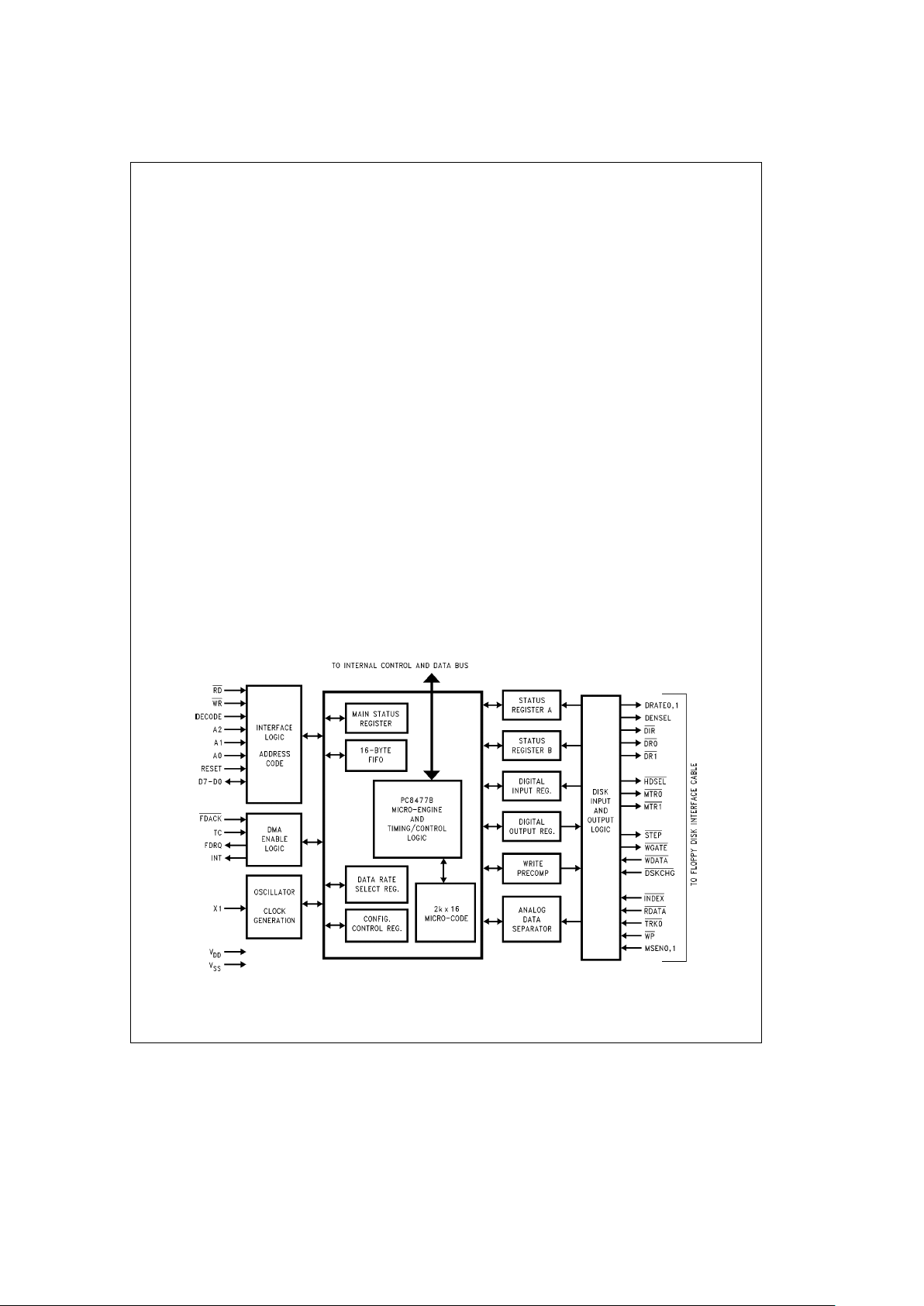
2.0 Configuration Registers (Continued)
3. Clear PTR bit 1 and then set PTR bit 0 (power-down)
high. See Section 2.5.3 PTR bits 0 and 1.
2.7 POWER-UP PROCEDURE AND CONSIDERATIONS
2.7.1 UART Power-Up
The clock signal to the UARTs is controlled through the
Configuration Registers (FER, PTR). In order to restore the
clock signal to one or both UARTs the following conditions
must exist:
1. The appropriate enable bit (FER 1,2) for the UART(s)
must be set
2. and the power-down bit (PTR 0) must not be set.
2.7.2 FDC Power-Up
The clock signal to the FDC is controlled through the Configuration Registers, the FDC Mode Command and the Data
Rate Select Register. In order to restore the clock signal to
the FDC the following conditions must exist:
1. The appropriate enable bit (FER 3) must be set
2. and the power-down bit (PTR 0) must not be set.
In addition to these conditions, one of the following must be
done to initiate the recovery from power-down mode:
1. Read the Main Status Register until the RQM bit (MSR7)
is set or
2. Write to the Data Rate Select Register and set the Software Reset bit (DSR7) or
3. Write to the Digital Output Register, clear and then set
the Reset bit (DOR2) or
4. Read the Data Register and the Main Status Register
until the RQM bit is set.
If the crystal has been stopped, read the RQM bit in the
Main Status Register until it is set. The RQM bit is not set
until the crystal has stabilized.
3.0 FDC Register Description
The floppy disk controller is suitable for all PC-AT, EISA,
PS/2, and general purpose applications. The operational
mode (PC-AT, PS/2, and Model 30) of the FDC is determined by bits 7, 6 of ASC register. AT mode is the default.
DP8473 and N82077 software compatibility is provided. Key
features include a 16-byte FIFO, PS/2 diagnostic register
support, perpendicular recording mode, CMOS disk interface, and a high performance analog data separator. See
Figure 3-1
.
The FDC supports the standard PC data rate drives of 250/
500 kbps, 300/500 kbps, and 1 Mbps in MFM-encoded data
mode, but is no longer guaranteed through functional testing to support the older FM encoded data mode. References to the older FM mode remain in this document to
clarify the true functional operation of the device.
The 1 Mbps data rate is used by the high performance tape
and floppy drives. The FDC supports these floppy drives
which utilize high density media, and require the perpendicular recording mode format. When used with the 1 Mbps
data rate, this new format allows the use of 4 MB floppy
drives which format Extra Density (ED) media to 2.88 MB
capacity.
The high performance internal analog data separator needs
no external components. It improves on the window margin
performance standards of the DP8473, and is compatible
with the strict data separator requirements of floppy disk
and floppy-tape drives.
The FDC contains write precompensation circuitry that defaults to 125 ns for 250 kbps, 300 kbps, and 500 kbps and
to 41.67 ns for 1 Mbps. These values can be overridden in
software to disable write precompensationn or to provide
levels of precompensation up to 250 ns.
TL/C/12379– 28
FIGURE 3-1. FDC Functional Block Diagram
27
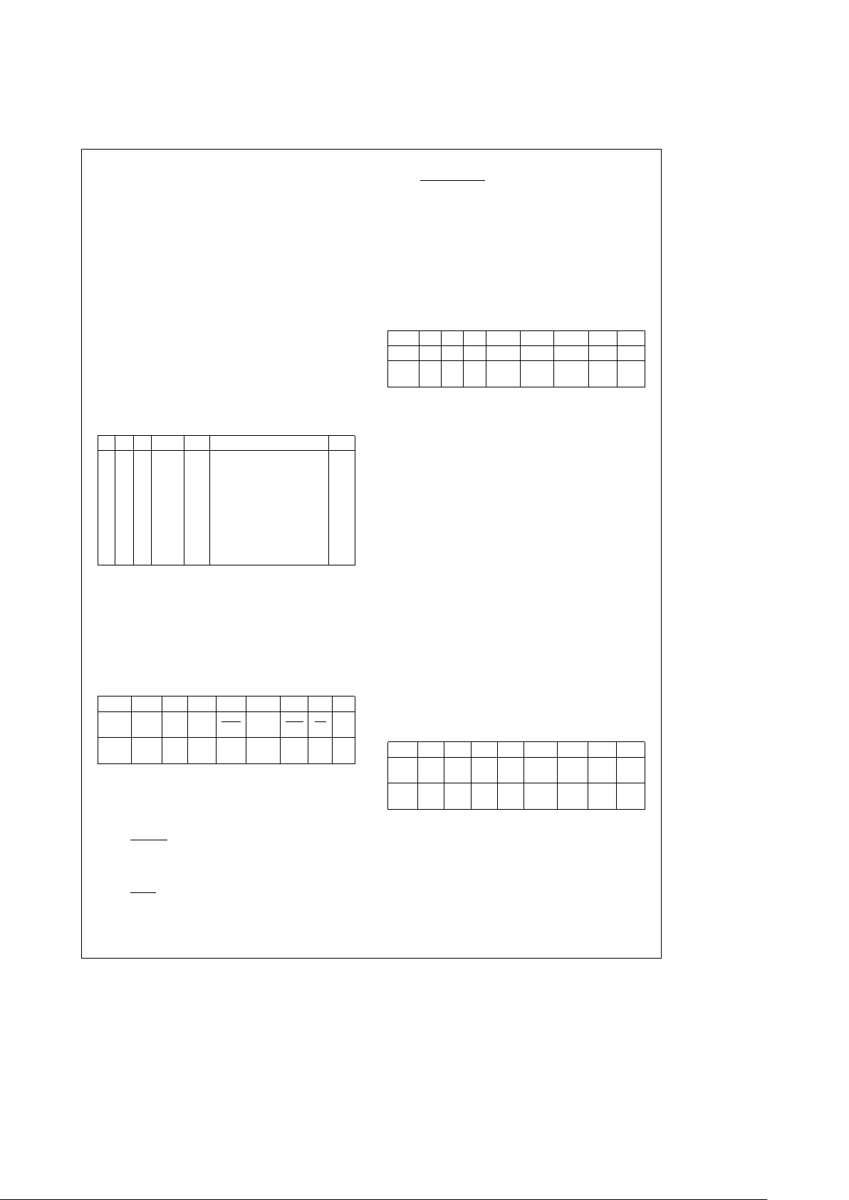
3.0 FDC Register Description (Continued)
The FDC has internal 24 mA data bus buffers which allow
direct connection to the system bus. The internal 40 mA
totem-pole disk interface buffers are compatible with both
CMOS drive inputs and 150X resistor terminated disk drive
inputs.
3.1 FDC CONTROL REGISTERS
The following FDC registers are mapped into the addresses
shown in Table 3-1 and described in the following sections.
The base address range is provided by the on-chip address
decoder pin. For PC-AT or PS/2 applications, the diskette
controller primary address range is 3F0 to 3F7h, and the
secondary address range is 370 to 377h. The FDC supports
three different register modes: the PC-AT mode, PS/2
mode (Micro Channel systems), and the Model 30 mode
(Model 30). See Section 5.2 for more details on how each
register mode is enabled. When applicable, the register definition for each mode of operation is given. If no special
notes are made, then the register is valid for all three register modes.
TABLE 3-1. Register Description and Addresses
A2 A1 A0 IDENT R/W Register
0 0 0 0 R Status Register A* SRA
0 0 1 0 R Status Register B* SRB
0 1 0 X R/W Digital Output Register DOR
0 1 1 X R/W Tape Drive Register TDR
1 0 0 X R Main Status Register MSR
1 0 0 X W Data Rate Select Register DSR
1 0 1 X R/W Data Register (FIFO) FIFO
1 1 0 X X None (Bus TRI-STATE)
1 1 1 X R Digital Input Register DIR
1 1 1 X W Configuration Control Register CCR
*Note: SRA and SRB are enabled by IDENTe0 during a chip reset only.
3.1.1 Status Register A (SRA) Read Only
This is a read-only diagnostic register that is part of the
PS/2 floppy controller register set, and is enabled when in
the PS/2 mode. This register monitors the state of the IRQ6
pin and some of the disk interface signals. The SRA can be
read at any time when in PS/2 mode. In the PC-AT mode,
D7–D0 are TRI-STATE during a mP read.
SRAÐPS/2 Mode
D7 D6 D5 D4 D3 D2 D1 D0
DESC IRQ6
RES STEP TRK0
HDSEL INDX WP DIR
PEND
RESET
0 N/A 0 N/A 0 N/A N/A 0
COND
D7 Interrupt Pending: This active high bit reflects the
state of the IRQ6 pin.
D6 Reserved.
D5 Step: Active high status of the STEP disk interface
output.
D4 Track 0
: Active low status of the TRK0 disk inter-
face input.
D3 Head Select: Active high status of the HDSEL disk
interface output.
D2 Index
: Active low status of the INDEX disk interface
input.
D1 Write Protect
: Active low status of the WP disk in-
terface input.
D0 Direction: Active high status of the DIR disk inter-
face output.
3.1.2 Status Register B (SRB) Read Only
This read-only diagnostic register is part of the PS/2 floppy
controller register set, and is enabled when in the PS/2
mode. The SRB can be read at any time when in PS/2
mode. In the PC-AT mode, D7 – D0 are TRI-STATE during a
mP read.
SRBÐPS/2 Mode
D7 D6 D5 D4 D3 D2 D1 D0
DESC 1 1 DR0 WDATA RDATA WGATE MTR1 MTR0
RESET
N/A N/A 0 0 0 0 0 0
COND
D7 Reserved: Always 1.
D6 Reserved: Always 1.
D5 Drive Select 0: Reflects the status of the Drive Se-
lect 0 bit in the DOR (address 2, bit 0). It is cleared
after a hardware reset, not a software reset.
D4 Write Data: Every inactive edge transition of the
WDATA disk interface output causes this bit to
change states.
D3 Read Data: Every inactive edge transition of the
RDATA disk interface output causes this bit to
change states.
D2 Write Gate: Active high status of the WGATE disk
interface output.
D1 Motor Enable 1: Active high status of the MTR1
disk interface output. Low after a hardware reset,
unaffected by a software reset.
D0 Motor Enable 0: Active high status of the MTR0
disk interface output. Low after a hardware reset,
unaffected by a software reset.
3.1.3 Digital Output Register (DOR) Read/Write
The DOR controls the drive select and motor enable disk
interface outputs, enables the DMA logic, and contains a
software reset bit. The contents of the DOR is set to 00h
after a hardware reset, and is unaffected by a software reset. The DOR can be written to at any time.
DOR
D7 D6 D5 D4 D3 D2 D1 D0
DESC MTR3 MTR2 MTR1 MTR0 DMAEN RESET
DRIVE DRIVE
SEL 1 SEL 0
RESET
0000 0 0 0 0
COND
D7 Motor Enable 3: This bit controls the MTR3 disk
interface output.A1inthis bit causes the MTR3 pin
to go active.
D6 Motor Enable 2: Same function as D7 except for
MTR2.
D5 Motor Enable 1: Same function as D7 except for
MTR1. (See bit 4 of FCR for further information.)
D4 Motor Enable 0: Same function as D7 except for
MTR0. (See bit 4 of FCR for further information.)
28

3.0 FDC Register Description (Continued)
D3 DMA Enable: This bit has two modes of operation.
PC-AT mode: Writinga1tothis bit enables the
FDRQ, FDACK
, TC, and IRQ6 pins. Writinga0to
this bit disables the FDACK
and TC pins and TRISTATE the FDRQ and the IRQ6 pins. This bit is a 0
after a reset when in these modes.
PS/2 mode: This bit is reserved, and the FDRQ,
FDACK
, TC, and IRQ6 pins are always enabled. Dur-
ing a reset, the FDRQ, FDACK
, TC, and IRQ6 lines
remain enabled, and D3 is 0.
D2 Reset Controller: Writinga0tothis bit resets the
controller. It remains in the reset condition until a 1
is written to this bit. A software reset does not affect
the DSR, CCR, and other bits of the DOR. A software reset affects the Configure and Mode command bits (see Section 4.0 FDC Command Set Description). The minimum time that this bit must be
low is 100 ns. Thus, toggling the Reset Controller bit
during consecutive writes to the DOR is an acceptable method of issuing a software reset.
D1, 0 Drive Select: These two bits are binary encoded for
the four drive selects DR0–DR3, so that only one
drive select output is active at a time. (See bit 4 of
FCR for further information.)
It is common programming practice to enable both the motor enable and drive select outputs for a particular drive.
Table 3-2 shows the DOR values to enable each of the four
drives.
TABLE 3-2. Drive Enable Values
Drive DOR Value
0 1Ch
12D
24E
38F
Note: The MTR3, MTR2, DRV3, DRV2 pins are only available in four-drive
mode (bit 4 of FER is 1) and require external logic.
3.1.4 Tape Drive Register (TDR) Read/Write
The TDR register is the Tape Drive Register and the floppy
disk controller media and drive type register. The register
has three modes of operation (see Table 3-3):
PC-AT Compatible mode. The register is used to assign a
particular drive number to the tape drive support mode of
the data separator. All other logical drives can be assigned
as floppy drive support. Bits 2– 7 are TRI-STATE during
read.
Automatic Media Sense mode. Bits 5 –7 are implemented,
in addition to the bits of the Compatible PC-AT TDR mode.
Bits 2 – 4 are reserved.
Enhanced mode. This is the PS/2 TDR mode. It uses all
the register’s bits for operation with PS/2 floppy drives.
The use of the TDR bits, for each of these modes, is shown
in Table 3-3.
D7 Extra Density: When bit 5 is 0, this media id bit is
used with bit 6 to indicate the type of media currently in the active floppy drive. If bit 5 is 1, it is invalid.
This bit holds MSEN1 pin value. See Table 3-4 for
details regarding bits 5 – 7.
D6 High Density: When bit 5 is 0, this media id bit is
used with bit 7 to indicate the type of media currently in the active floppy drive. If bit 5 is 1, it is invalid.
This bit holds MSEN0 pin value. See Table 3-4 for
details regarding bits 5 – 7.
TABLE 3-3. TDR Operation Modes
Mode
FCR ASC
Bit D7 D6 D5 D4 D3 D2 D1 D0
Bit 0 Bit 2
PC-AT Compatible 1 0
DESC XX X X X X
TAPE TAPE
SEL 1 SEL 0
RESET
N/A N/A N/A N/A N/A N/A 0 0
COND
Automatic Media Sense 0 0
DESC ED HD
VALID
XX X
TAPE TAPE
DATA SEL 1 SEL 0
RESET
N/A N/A N/A N/A N/A N/A 0 0
COND
Enhanced or
1
0
1
DESC ED HD
VALID
X SWP1 SWP0
TAPE TAPE
DATA SEL 1 SEL 0
RESET
N/A N/A N/A 1 0 0 0 0
COND
29
3.0 FDC Register Description (Continued)
D5 Valid Data:
Automatic Media Sense mode: The state of bit 5
is determined by the state of the VLD0,1
bits in the
ASC Configuration Register. If this bit is 0, there is
valid media id sense data in bits 7 and 6 of this
register. Bit 5 holds VLD0
when drive 0 is accessed,
and media sense is configurfed. It holds VLD1
when
drive 1 is accessed, and media sense is configured.
Otherwise, it is set to 1 to indicate that media information is not available. Valid data should be used
only when accessing drives 0 and 1. See Table 3-4
for details regarding bits 5 –7.
PC-AT Compatible mode: When four drive encoding is used (FER4
e
1), this bit is set to 1.
TABLE 3-4. Media ID Bits Functions
Bit 7 Bit 6 Bit 5 Media Type
X X 1 Invalid Data
0 0 0 5.25
×
0 1 0 2.88M
1 0 0 1.44M
1 1 0 720k
D4 Reserved.
D3, 2 Bits 3 and 2 are read/write bits that control bits con-
trol logical drive exchange.
When working with four drives encoding (bit 4 of
FER is 1) the logical drive exchange is not performed.
00: No logical drive exchange.
01: Logical drive exchange between drives 0 and 1.
DR1
internal signal to DR0 pin.
MTR1 internal signal to MTR0 pin.
DR0 internal signal to DR1 pin.
MTR0 internal signal to MTR1 pin.
10: Logical drive exchange between drives 0 and 2.
The DR0
and MTR0 pins function is exchanged
as follows:
DR2
internal signal to DR0 pin.
MTR2 internal signal to MTR0 pin.
11: Reserved. Unpredictable results when 11 is
configured.
D1, 0 Tape Select 1, 0: These bits assign a logical drive
number to a tape drive. Drive 0 is not available as a
tape drive and is reserved as the floppy disk boot
drive. See Table 3-5 for the tape drive assignment
values.
TABLE 3-5. Tape Drive Assignment Values
TAPESEL1 TAPESEL0
Drive
Selected
0 0 None
011
102
113
3.1.5 Main Status Register (MSR) Read Only
The read-only Main Status Register indicates the current
status of the disk controller. The Main Status Register is
always available to be read. One of its functions is to control
the flow of data to and from the Data Register (FIFO). The
Main Status Register indicates when the disk controller is
ready to send or receive data through the Data Register. It
should be read before each byte is transferred to or from
the Data Register except during a DMA transfer. No delay is
required when reading this register after a data transfer.
After a hardware or software reset, or recovery from a power-down state, the Main Status Register is immediately
available to be read by the mP. It contains a value of 00h
until the oscillator circuit has stabilized, and the internal registers have been initialized. When the FDC is ready to receive a new command, it reports an 80h to the mP. The
system software can poll the MSR until it is ready. The worst
case time allowed for the MSR to report an 80h value (RQM
set) is 2.5 ms after reset or power up.
MSR
D7 D6 D5 D4 D3 D2 D1 D0
DESC RQM DIO NON CMD DRV3 DRV2 DRV1 DRV0
DMA PROG BUSY BUSY BUSY BUSY
RESET
0000 0000
COND
D7 Request for Master: Indicates that the controller is
ready to send or receive data from the mP through
the FIFO. This bit is cleared immediately after a byte
transfer and is set again as soon as the disk controller is ready for the next byte. During a Non-DMA
Execution phase, the RQM indicates the status of
the interrupt pin.
D6 Data I/O (Direction): Indicates whether the con-
troller is expecting a byte to be written to (0) or read
from (1) the Data Register.
D5 Non-DMA Execution: Indicates that the controller
is in the Execution Phase of a byte transfer operation in the Non-DMA mode. This mode can be used
for multiple byte transfers by the mP in the Execution Phase via interrupts or software polling.
D4 Command in Progress: This bit is set after the first
byte of the Command Phase is written. This bit is
cleared after the last byte of the Result Phase is
read. If there is no Result Phase in a command, the
bit is cleared after the last byte of the Command
Phase is written.
D3 Drive 3 Busy: Set after the last byte of the Com-
mand Phase of a Seek or Recalibrate command is
issued for drive 3. Cleared after reading the first
byte in the Result Phase of the Sense Interrupt
Command for this drive.
D2 Drive 2 Busy: Same as above, but for drive 2.
D1 Drive 1 Busy: Same as above, but for drive 1.
D0 Drive 0 Busy: Same as above, but for drive 0.
30
 Loading...