NSC PC87200VUL Datasheet
PC87200 PCI to ISA Bridge
© 1999 National Semiconductor Corporation
www.national.com
August 1999
PC87200 PCI to ISA Bridge
1.0 General Description
The PC87200 Enhanced Integrated PCI-to-ISA bridge
works with an LPC chipset to provide ISA slot support. It is
a complement to the National Semiconductor PC8736x
Super I/O family.
2.0 Features
2.1 General
– Functionally compatible with Intel 82380AB
– 5.0 V tolerant PCI and ISA interfaces
– Slave mode serializedIRQ support for both quiet and
continuous modes
– PC/PCI DMA support
– 32-bit address decode for the 1MB BIOS ROM
– Supports ISA bus mastering
– 160-pin PQFP package
2.2 PCI-to-ISA Bridge
– PCI 2.1 compliant 33 MHz bus
– Supports PCI initiator-to-ISA and ISA master-to-PCI
cycle translations
– Subtractive agentforunclaimed transactions(seethe
PROHIBIT signal description for exceptions)
– Parallel to Serial IRQ conversion including
IRQ3,4,5,6,7,9,10,11,12,14,15
– Supports 4 ISA slots directly without buffering
– Programmable ISA clock (8.33 to 11 MHz)
– Slow slew rate on edges
2.3 "PROHIBIT" functional support
– Disables PCI bus subtractive decoding when PRO-
HIBIT is asserted
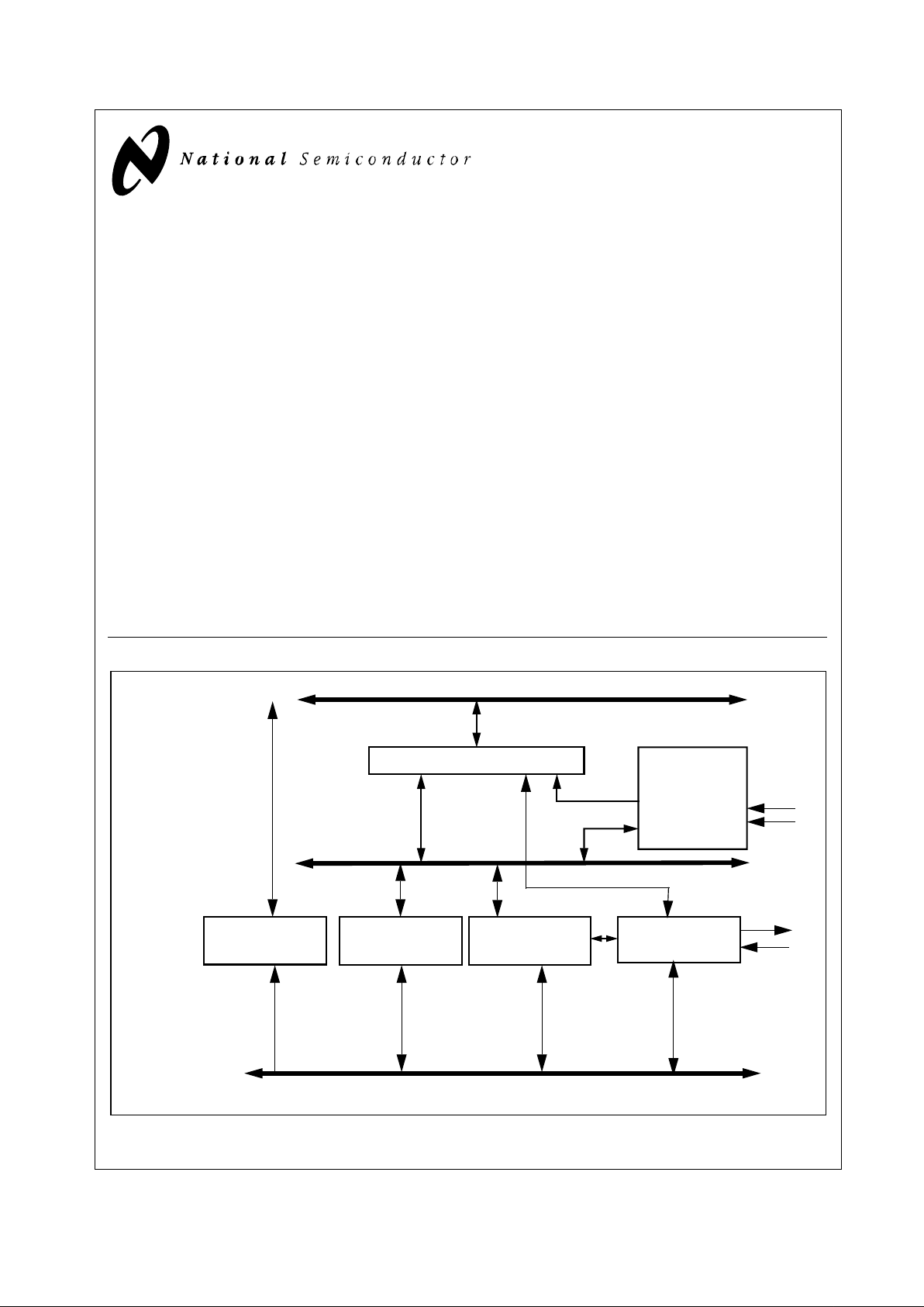
Block Diagram
X-Bus
ISA Bus
PCI Bus
PCI to X-Bus / X-Bus to PCI Bridge
PCI Configuration
Registers
X-Bus Arbiter
PC87200 Support
Serial IRQ Slave
mode interface logic
Serialized IRQ
Interface
PC/PCI DMA
Interface
ISA bus Target
Interface
ISA bus Master
Interface
PCPCIREQ#
PCPCIGNT#
Decoding logic
BPD#
PROHIBIT
TRI-STATE® is a registered trademark of National Semiconductor Corporation.

2 www.national.com
Table of Contents
1.0 General Description . . . . . . . . . . . . . . . . . . . . . . . . . . . .1
2.0 Features . . . . . . . . . . . . . . . . . . . . . . . . . . . . . . . . . . . . . .1
2.1 General . . . . . . . . . . . . . . . . . . . . . . . . . . . . . . . . .1
2.2 PCI-to-ISA Bridge . . . . . . . . . . . . . . . . . . . . . . . . . 1
2.3 "PROHIBIT" functional support . . . . . . . . . . . . . . . 1
3.0 Device Overview . . . . . . . . . . . . . . . . . . . . . . . . . . . . . . .3
3.1 PCI Bus Interface . . . . . . . . . . . . . . . . . . . . . . . . . .3
3.2 ISA Bus Interface . . . . . . . . . . . . . . . . . . . . . . . . . . 3
3.3 Serialized IRQ support . . . . . . . . . . . . . . . . . . . . . .3
3.4 PROHIBIT signal support . . . . . . . . . . . . . . . . . . .5
3.5 PC/PCI DMA Interface Support . . . . . . . . . . . . . . . 5
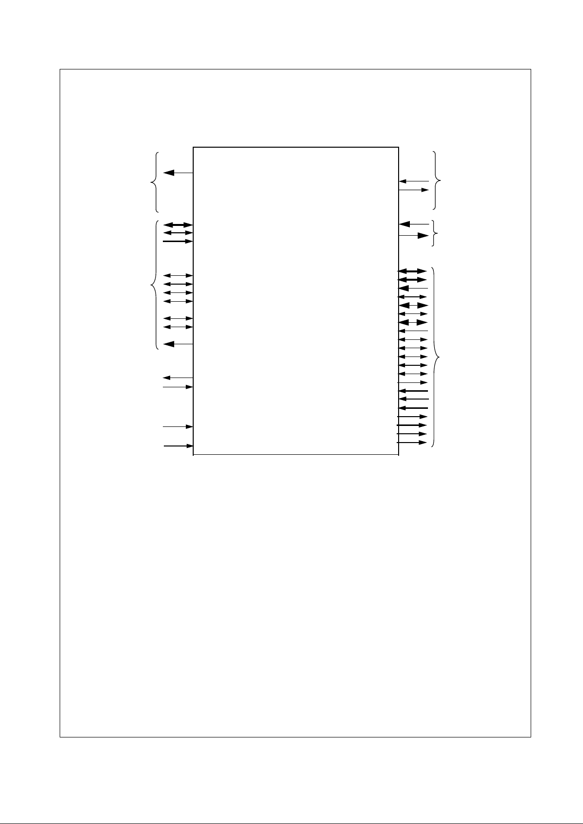
4.0 Device Pinout . . . . . . . . . . . . . . . . . . . . . . . . . . . . . . . . . 7
5.0 Pin Descriptions . . . . . . . . . . . . . . . . . . . . . . . . . . . . . . . 8
5.1 Signal Definitions . . . . . . . . . . . . . . . . . . . . . . . . . .8
5.2 Pin Assignments . . . . . . . . . . . . . . . . . . . . . . . . . .9
5.3 Signal Descriptions . . . . . . . . . . . . . . . . . . . . . . . .9
6.0 Configuration . . . . . . . . . . . . . . . . . . . . . . . . . . . . . . . .15
7.0 Register Descriptions . . . . . . . . . . . . . . . . . . . . . . . . .16
7.1 Register Summary . . . . . . . . . . . . . . . . . . . . . . . .16
7.2 Chipset Register Space . . . . . . . . . . . . . . . . . . . .17
8.0 Electrical Characteristics . . . . . . . . . . . . . . . . . . . . . . .22
8.1 Electrical Specifications . . . . . . . . . . . . . . . . . . . .22
8.2 PC87200Test Modes . . . . . . . . . . . . . . . . . . . . . .22
8.3 Electrical Connections . . . . . . . . . . . . . . . . . . . . . 29
8.4 Absolute Maximum Ratings . . . . . . . . . . . . . . . . .29
8.5 Recommended Operating Conditions . . . . . . . . .29
8.6 DC Characteristics . . . . . . . . . . . . . . . . . . . . . . .30
8.7 AC Characteristics . . . . . . . . . . . . . . . . . . . . . . . .31
9.0 Physical Dimensions . . . . . . . . . . . . . . . . . . . . . . . . . . 33
3 www.national.com
3.0 Device Overview
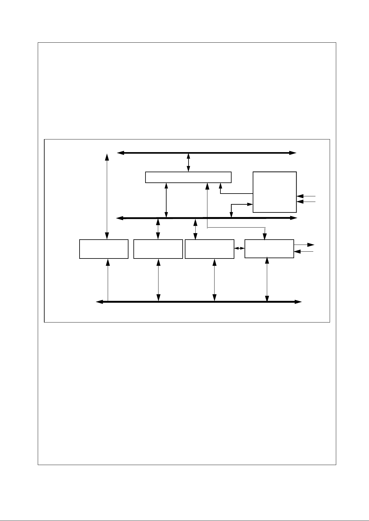
The PC87200 can be described as providing the functional
blocks shown in Figure 1.
— PCI bus master/slave interface
— ISA bus master/slave interface
— Serial IRQ slave mode interface
— PROHIBIT signal support
— PC/PCI DMA interface
3.1 PCI Bus Interface
The PC87200 provides a PCI bus interface that is both a
slave for PCI cycles initiated by the CPU or other PCI mas-
ter devices, and a PC/PCI DMA master for DMA transfer
cycles. The PC87200 supports positive decode for the
BIOS ROM in the special test mode and implements subtractive decode for unclaimed PCI accesses when the
PROHIBIT signal is low. The PC87200 also generates
address and data parity and performs parity checking.
Configuration registers are accessed through the PCI interface using the PCI Bus Type 1 configuration mechanism as
described in the PCI 2.1 Specification.
3.2 ISA Bus Interface
The PC87200 provides an ISA bus interface for subtractive-decoded memory and I/O cycles on PCI. The
PC87200 is the default subtractive decoding agent and will
forward all unclaimed memory and I/O cycles to the ISA
interface; however, the PC87200 may be configured to
ignore either I/O, memory or all unclaimed cycles (subtractive decode disabled) by asserting the PROHIBIT signal.
ISA master cycles will only be passed to the PCI bus if they
access memory. I/O accesses are left to complete on the
ISA bus.
ISA master cycles that access memory on ISA bus are not
supported by the PC87200.
3.3 Serialized IRQ support
The PC87200’s Serial Interrupt interface uses a serial
interrupt bus to transmit ISA Bus legacy interrupt requests.
The bus is a one pin bus(SERIRQ) and uses the PCI clock
as its timing reference. The serial interrupt bus is a multidrop bus that is shared by all PCI devices that have legacy
interrupts. The serial interrupt logic conforms to the serial-
ized IRQ defined in the Serialized IRQ on the “PCI way” Version 6.0 specification. Programming of the serial interrupt controller when the controller is currently running can
produce unexpected results.
X-Bus
ISA Bus
PCI Bus
PCI to X-Bus / X-Bus to PCI Bridge
PCI Configuration
Registers
X-Bus Arbiter
PC87200 Support
Serial IRQ Slave
mode interface logic
Serialized IRQ
Interface
PC/PCI DMA
Interface
ISA bus Target
Interface
ISA bus Master
Interface
PCPCIREQ#
PCPCIGNT#
Decoding logic
BPD#
PROHIBIT
Internal Block Diagram
3.0 Device Overview (Continued)
4 www.national.com
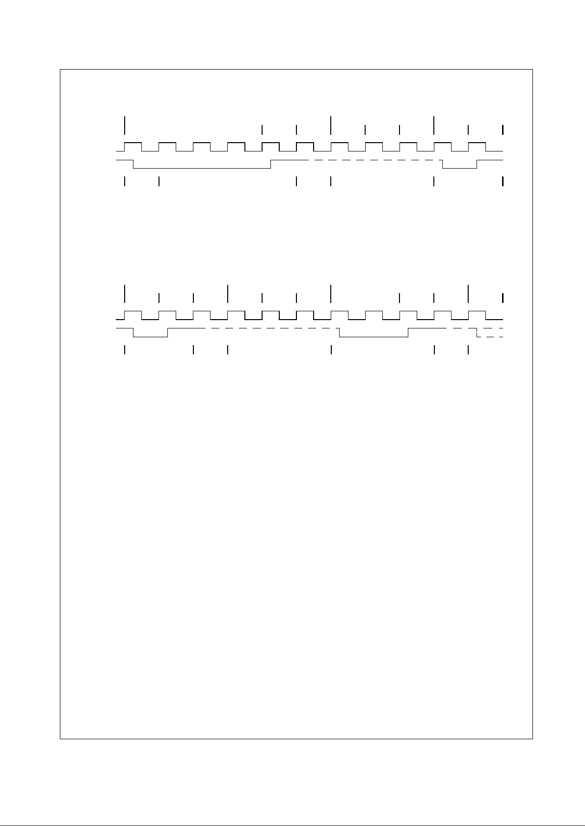
Timing of the serialized IRQ is illustrated as follows.
3.3.1 Serial Interrupts (Slave Mode)
There are two types of Serial Interrupt transfer modes; the
following describes the operation of the PC87200’s Serial
Interrupt Interface as a Slave:
1. Quiet Mode: Any Serial Interrupt device may initiate a
Start Cycle, while theSerial Interruptinterface isIdle, by
driving SERIRQ low for one PCI clock period. After driving lowfor one clock the device should immediately TRI-
STATE
®
SERIRQ, without ever driving this signal high.
A Start Cycle may not be initiated in the middleof an active Serial Interrupt transfer.Between Stopand Start Cycles the SERIRQsignal willbe pulled highand theSerial
Interrupt interface will be Idle.
When the PC87200 Serial Interrupt interface must initiate a Start Cycle in order to transfer any pending interrupt request to the Master. The only exception to this
requirementis whenaSerial Interrupttransfer sequence
is already in progressand the PC87200 can transferthe
request during this present Serial Interrupt transfer sequence,then the SerialInterrupt device isnotrequired to
generate another Start Cycle.
2. Continuous Mode: The PC87200 tracks both the Start
and Stop Frames and is responsible for inserting its interrupt requests on the appropriate IRQ frames.
3.3.2 IRQ Sampling Periods
Once a Start Cycle has been initiated all Serial Interrupt
devices watch for the rising edge of the Start Pulse and
start counting IRQ Sample periods from that point. Each
IRQ Sample Period is three clocks long, with the first clock
being the Sampled phase, the second clock being the
Recovery phase, and the third clock being the Turn-around
phase. During the Sample phase the Serial Interrupt
device drives SERIRQ low if its associated IRQ signal/data
is presently low. If its IRQ signal/data is high the Serial
Interrupt device must TRI-STATE SERIRQ. During the
Recovery phase, the Serial Interrupt device that drove
SERIRQ low (if any Serial Interface device does) is
required to drive back high. During the Turn-around phase
all Serial Interface devices will TRI-STATE SERIRQ. All
Serial Interface devices will drive SERIRQ low at the
appropriate sample point regardless of which device initiated the sample activity, if its associated IRQ signal/data is
low.
Slave
The PC87200 will support the interrupt request frames
listed in the following table.
The Generation clock for each IRQ follows the low to high
edge of the Start Pulse by the number of PCI Clocks listed
in Table 1.
Note: : The number of clocks equals: (3 x (IRQ number + 1)) - 1
3.3.3 Stop Cycle Control
The PC87200 will monitor SERIRQ for a Stop Cycle, so
that it may initiate a Start Cycle for a pending transition in
any of its IRQs (Quiet Mode). For Continuous Mode, the
PC87200 will not initiate any Start Cycle, but will track the
Start and Stop Cycles and insert its IRQs appropriately.
PCI CLK
SERIRQ
START R T S R T S R
START CYCLE
START
Driving
Source
Slave (Q)
Master (C)
Master NONE NONE IRQ1 Source
IRQ0 IRQ1
R = Recovery; T= Turn-around; S = Sample
Start Cycle Timing
PCI CLK
SERIRQ
RTSRTTR
STOP CYCLE
Driving
Source
IRQ15 Source MasterNONE NONE NONE
IRQ15
R = Recovery; T= Turn-around; S = Sample
S
STOP
(NOTE 1)
START
IOCHK#
NOTE 1: The Stop pulse is 2 clocks wide for Quiet mode, 3 clocks wide for Continuous mode
Stop Cycle Timing
3.0 Device Overview (Continued)
5 www.national.com
3.4 PROHIBIT signal support
The chipset will use this signal to claim the BIOS first and
then deassert the "PROHIBIT" signal to configure the PCI
to ISA bridge to continue the boot sequence.
Special test mode support is provided by means of the
BPD# pin. When this test mode is active, the PC87200 will
enable positive memory decode during boot up to enable
the host to look for boot ROM on ISA card.
PROHIBIT will be a don’t care in this test mode at boot up
for the ROM BIOS range, but should function normally after
booting
3.5 PC/PCI DMA Interface Support
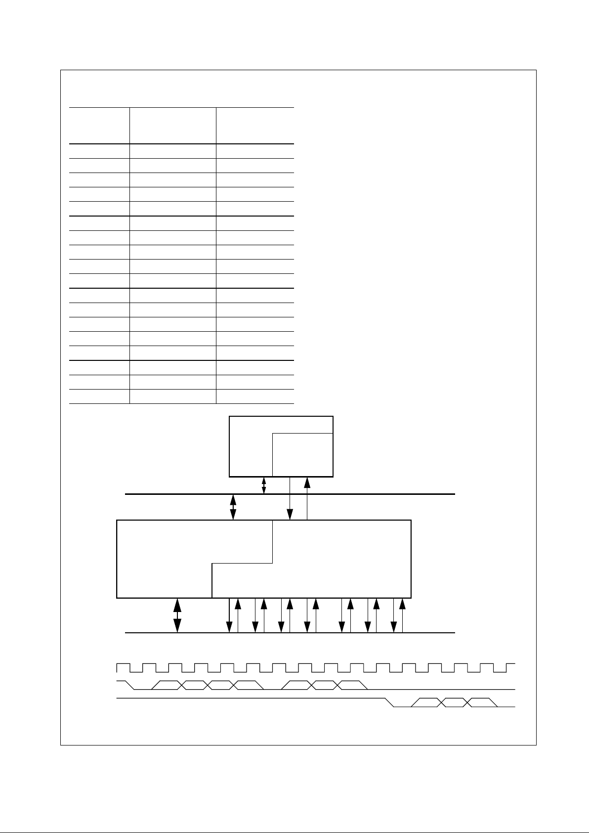
The PC87200 operatesas a PC/PCI DMA Secondary Arbitration Bridge. The PC87200 can passall seven legacy ISA
bus DMA channel requests to the PC/PCI DMA Primary
Bus Arbiter using the channel passing protocol defined in
the Moble PC/PCI DMA Arbitration and Protocol Specification (Revision 2.2). Figure 1 shows the topology of the
PC87200 PC/PCI DMA requests and grants:
The PC87200 converts the seven legacy ISA bus DMA
requests (DREQ0, 1, 2, 3, 5, 6 and 7) into a serial PC/PCI
DMA compliant REQ# sequence and converts the corresponding PC/PCI DMA GNT# sequence into the appropriate DMAacknowledge (DACK0-3, 5-7#). ThisPC/PCI DMA
expansion Channel Passing Protocol is illustrated
Figure 2.
Table 1. SERIRQ Slave Generation Periods
SERIRQ
Period
Signal Generated
# of clocks past
Start
1 Reserved. 2
2 Reserved. 5
3 Reserved. 8
4 IRQ3 11
5 IRQ4 14
6 IRQ5 17
7 IRQ6 20
8 IRQ7 23
9 Reserved. 26
10 IRQ9 29
11 IRQ10 32
12 IRQ11 35
13 IRQ12 38
14 Reserved. 41
15 IRQ14 44
16 IRQ15 47
17 IOCHK# 50
21:18 Reserved. 62,59,56, 53
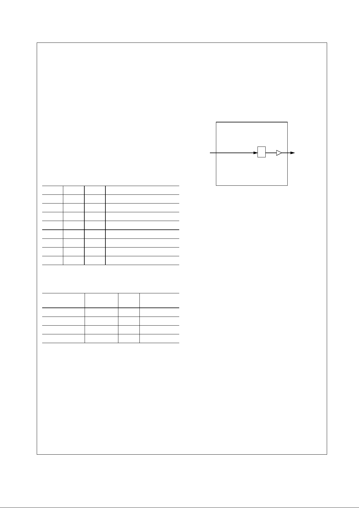
Figure 1. PC87200 PC/PCI DMA Topology
Figure 2. Channel Passing Protocol
PC/PCI DMA
Primary Bus
Arbiter
PCI Bus
PCPCIREQ#
PCPCIGNT#
PC87200
DACK0#
DREQ0
DACK1#
DREQ1
DACK2#
DREQ2
DACK3#
DREQ3
DACK5#
DREQ5
DACK6#
DREQ6
DACK7#
DREQ7
PC/PCI DMA Interface Support
ISA Bus
start
CH0
CH1
CH2 CH3 CH4 CH5 CH6
CH7
start
bit 0 bit 1 bit 2
PCICLK
PCPCIREQ#
PCPCIGNT#
3.0 Device Overview (Continued)
6 www.national.com
When a legacy ISA bus DMA request is asserted, the
PC87200 will transmit that request to the PC/PCI Primary
Bus Arbiter by encoding it and driving it out the PC87200’s
PCPCIREQ# according to the above; first PCPCIREQ# will
be driven low for one PCICLK period to indicate that the
serial encoded request transfer is starting. Then the
PC87200 willdrive each ofthe next eight bits with the value
of its corresponding DREQ. (NOTE: Channel 4 will always
be driven low.) At the end of the request sequence, the
PC87200 will continue to drive its PCPCIREQ# signal
active, indicating that the request is still being maintained.
In response to the request sequence, the PC/PCI Primary
Bus Arbiter will respond with a PC/PCI DMA encoded grant
transfer when it is granting the PCI bus for a PC/PCI DMA
transfer cycle. The PC/PCI encoded grant transfer will
begin when the PC/PCI Primary Bus Arbiter drives
PCPCIGNT# low for one PCICLK period to indicate the
start of the grant sequence; then the next three
PCPCIGNT# signal PCICLK periods will then contain the
encoded grant value, indicating which legacy ISA DMA
channel is being granted the PC Bus.
After receiving a valid grant from the PC/PCI DMA Arbiter,
the PC87200 will recognize the following I/O accesses as
DMA I/O Reads(Writes) from (to) the granted legacy ISA
DMA channel.
PCI bus address bit 2 (A2) indicates if the cycle is to be a
Terminal Count cycle or not.
For Normal DMA Cycles, PCI bus I/O Reads and Writes
will be translated to legacy ISA DMA Reads and Writes
respectively. For Verify DMA Cycles, only PCI bus I/O
Reads will be translated to legacy ISA DMA Verify cycles.
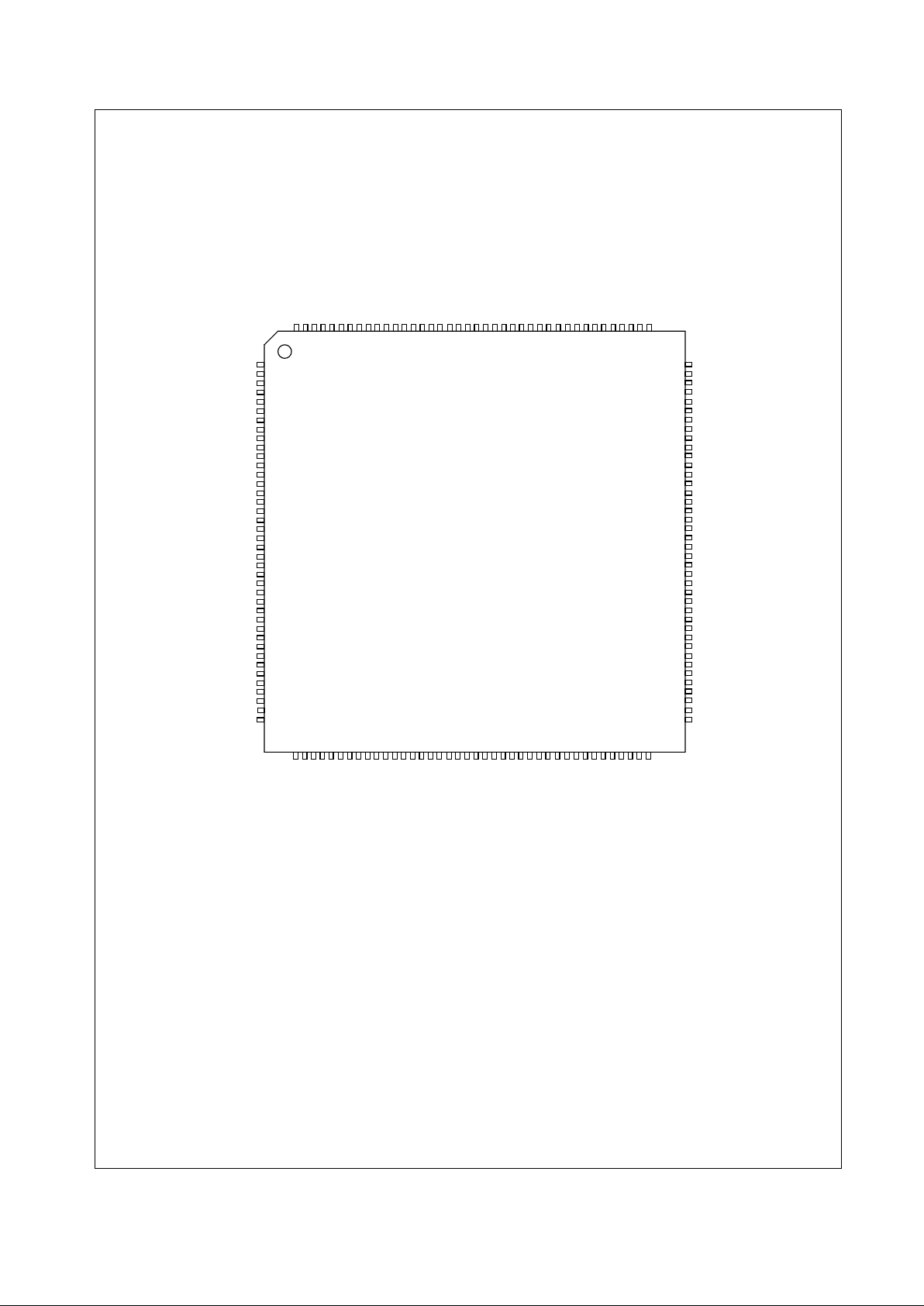
3.5.4 Clock Generation
The PC87200 generates the ISA clock using PCI clock signal (typically 33 MHz).
A PCICLK divisor (3,4) is programmable through PCI configuration register to generate the ISA clock signal. This
provides support for the generation of ISACLK frequencies
8.33 MHz and 11 MHz off of a 33MHz PCICLK.
Figure 3. showsa block diagramfor clock generation within
the PC87200.
bit 2 bit 1 bit 0 Channel Granted
0 0 0 DMA Channel 0 (DACK0#)
0 0 1 DMA Channel 0 (DACK1#)
0 1 0 DMA Channel 0 (DACK2#)
0 1 1 DMA Channel 0 (DACK3#)
1 0 0 RESERVED
1 0 1 DMA Channel 0 (DACK5#)
1 1 0 DMA Channel 0 (DACK6#)
1 1 1 DMA Channel 0 (DACK7#)
DMA Cycle
Type
DMA
I/O Address
TC (A2) PCI Cycle Type
Normal 0000_0000h 0 I/O Read/Write
Normal TC 0000_0004h 1 I/O Read/Write
Verify 0000_00C0h 0 I/O Read
Verify TC 0000_00C4h 1 I/O Read.
Figure 3. PC87200 Clock Generation
N
SYSCLKPCICLK
PC87200
7 www.national.com
4.0 Device Pinout
AD31
1
2
3
4
5
6
7
8
9
10
11
12
13
14
15
16
17
18
19
20
21
22
23
24
25
26
27
28
29
30
31
32
33
34
35
36
37
38
39
40
414243444546474849505152535455565758596061626364656667686970717273747576777879
80
120
119
118
117
116
115
114
113
112
111
110
109
108
107
106
105
104
103
102
101
100
99
98
97
96
95
94
93
92
91
90
89
88
87
86
85
84
83
82
81
160
159
158
157
156
155
154
153
152
151
150
149
148
147
146
145
144
143
142
141
140
139
138
137
136
135
134
133
132
131
130
129
128
127
126
125
124
123
122
121
Vdd
Vss
SA18
SA19
DACK2#
DREQ2
SYSCLK
SD7
SD6
SD5
SD4
IOCHK#
SD3
SD2
SD1
SD0
Vdd
Vss
IOCHRDY
SMEMR#
AEN
SMEMW#
IOR#
IOW#
MEMCS16#
IOCS16#
SA20
SA21
SA22
SA23
IRQ10
IRQ11
IRQ9
IRQ12
IRQ15
IRQ14
Vdd
Vss
DACK0#
DREQ0
MEMR#
MEMW#
DACK5#
DREQ5
SD8
SD9
SD10
SD11
DACK6#
DREQ6
SD12
SD13
SD14
SD15
DACK7#
DREQ7
Vdd
Vss
MASTER#
SBHE#
TC
BPD#
AD30
AD29
AD28
AD27
AD26
Vdd
Vss
C/BE3#
IDSEL
AD23
AD22
AD25
AD24
Vdd
Vss
AD0
AD1
AD2
AD3
AD4
AD5
Vss
Vdd
AD6
AD7
C/BE0#
AD8
AD9
AD10
Vss
Vdd
AD11
AD12
AD13
AD14
AD15
C/BE1#
Vss
Vdd
PAR
SERR#
STOP#
DEVSEL#
TRDY#
IRDY#
Vss
Vdd
FRAME#
C/BE2#
AD16
AD17
AD18
AD19
AD20
AD21
SA17
SA16
SA15
SA14
SA13
SA12
SA11
SA10
SA9
Vss
Vdd
SA8
SA7
SA6
SA5
SA4
SA3
SA2
SA1
SA0
Vss
Vdd
PROHIBIT
DREQ1
DACK1#
RSTDRV
DREQ3
DACK3#
IRQ7
IRQ6
IRQ5
IRQ4
IRQ3
SERIRQ
PCPCIGNT#
PCPCIREQ#
PCIRST#
PCICLK
Vss
Vdd
BALE
REFRESH#
8 www.national.com
5.0 Pin Descriptions
5.1 Signal Definitions
This section defines the signals and describes the external interface of the PC87200. The following diagram shows the
pins organized by their functional groupings. Internal test and electrical pins are not shown.
AD[31:0]
C/BE[3:0]#
PAR
FRAME#
TRDY#
STOP#
DEVSEL#
SERR#
IDSEL
SERIRQ
PCI Bus
IRQ Interface
IRDY#
PCICLK
SYSCLK
Clocks
Reset
PCIRST#
PC87200
SA[23:0]
IOCHK#
SBHE#
BALE
IOCHRDY
REFRESH#
IOR#
IOW#
MEMCS16#
MEMR#
MEMW#
AEN
DREQ[7:5], [3:0]
DACK#[7:5], [3:0]
TC
IRQ[15:14], [12:9], [7:3]
ISA Bus
IOCS16#
SD[15:0]
SMEMW#
SMEMR#
Serialized
PROHIBIT
MASTER#
BPD#
RSTDRV
PC87200 Signal Groups
PCPCIGNT#
PCPCIREQ#
Enhanced Integrated PCI-to-ISA
Bridge

9 www.national.com
5.0 Pin Descriptions (Continued)
5.2 Pin Assignments
The tables in this section use several common abbreviations. Table 2. lists the mnemonics and their meanings.
In the next section, description of each signal within its associated functional group is provided.
5.3 Signal Descriptions
5.3.1 Reset Signals
5.3.2 Clock Interface Signals
Table 2. Pin Type Definitions
Mnemonic Definition
I Standard input pin.
I/O Bidirectional pin.
O Totem-pole output.
OD Open-drain output structure that allows multiple devices to share the pin in a wired-OR configuration.
PU Pull-up resistor.
PD Pull-down resistor.
smt Schmitt Trigger.
s/t/s Sustained TRI-STATE, an active-low TRI-STATE signal owned and driven by one and only one agent at a
time. The agent that drives an s/t/s pin low must drive it high for at least one clock before letting it float. A
new agent cannot start drivingan s/t/ssignal anysooner thanone clockafter theprevious owner lets it float.
A pull-up resistor is required to sustain the inactive state until another agent drives itand must be provided
by the central resource.
t/s TRI-STATE signal.
VDD (PWR) Power pin.
VSS (GND) Ground pin.
# The"#" symbolat theend of asignal name indicatesthatthe active,orasserted stateoccurs whenthe signal
is at a lowvoltage level. When "#" is not presentafter thesignal name, the signal isasserted whenat a high
voltage level.
Signal Name Pin
No.
Type Description
PCIRST# 124 I PCI Reset
PCIRST# is the reset signal for the PCI bus.
RSTDRV 135 O Reset Drive
This signal is asserted to reset devices that reside on the ISA bus. It will be driven
by the inverse of the PCIRST# input signal.
Signal Name Pin No. Type Description
PCICLK 123 I PCI Clock
This clock runs at the PCI clock frequency and is used to drive most of the
PC87200 circuitry.
SYSCLK 8 O ISA Bus Clock
ISACLK is derived from PCICLK and is typically programmed for 8.33MHz.
F0 Index 50h[2:0]is usedto program the ISA clockdivisor. Thesebits determine
the divisor of the PCI clock used to generate the ISA bus clock. If F0 Index
50h[2:0] is set to:
010 = Divide by three (sysclk=11MHz)
011 = Divide by four (sysclk = 8.33MHz)
All other values are invalid and can produce unexpected results.

10 www.national.com
5.0 Pin Descriptions (Continued)
5.3.3 PCI Interface Signals
Signal Name Pin No. Type Description
AD[31:0] 65,66,
67,68,
69,70,
73,74,
77,78,
81,82,
83,84,
85,86,
100,101,
102,103,
104,107,
108,109,
111,112,
115,116,
117,118,
119,120
I/O
t/s
PCI Address/Data
AD[31:0] is a physicaladdress duringthe firstclock ofa PCI transaction; it is the
data during subsequent clocks.
When the PC87200 is a PCI master, AD[31:0] are outputs during the address
and write data phases, and are inputs during the read data phase of a transaction.
When the PC87200 is a PCI slave, AD[31:0] are inputs during the address and
write data phases, and are outputs during the read data phase of a transaction.
C/BE[3:0]# 75,87,
99,110
I/O
t/s
PCI Bus Command and Byte Enables
During the address phaseof aPCI transaction, C/BE[3:0]# defines the bus com-
mand. During the data phase of a transaction, C/BE[3:0]# are the data byte enables.
C/BE[3:0]# are outputs whenthe PC87200is aPCI master and are inputs when
it is a PCI slave.
IDSEL 76 I Initialization Device Select
It is used as a chip select during configuration read and write transactions.
FRAME# 88 I/O
t/s
PCI Cycle Frame
FRAME# is assertedto indicatethe startand durationof a transaction. It isdeas-
serted on the final data phase.
FRAME# is an input when the PC87200 is a PCI slave.
IRDY# 91 I/O
t/s
PCI Initiator Ready
IRDY#is drivenbythe masterto indicatevalid data ona write transaction,or that
it is ready to receive data on a read transaction.
When the PC87200 is a PCI slave, IRDY# is an input that can delay the begin-
ning of a write transaction or the completion of a read transaction.
Wait cycles are inserted until both IRDY# and TRDY# are asserted together.
TRDY# 92 I/O
t/s
PCI Target Ready
TRDY# is asserted by a PCIslave to indicate it is ready tocomplete the current
data transfer.
TRDY# is an input that indicates a PCI slave has driven valid data on a read or
a PCI slave is ready to accept data from the PC87200 on a write.
TRDY# is an output that indicates the PC87200 has placed valid data on
AD[31:0] during a read or is ready to accept the data from a PCI master on a
write.
Wait cycles are inserted until both IRDY# and TRDY# are asserted together.
STOP# 94 I/O
t/s
PCI Stop
As an input, STOP# indicates that a PCI slave wants to terminate the current
transfer. The transfer will be aborted, retried, or disconnected.
As anoutput, STOP# is asserted withTRDY# to indicate a targetdisconnect, or
without TRDY# to indicate a target retry.
 Loading...