NSC PC8477BV-1 Datasheet
PC8477B (SuperFDCTM)
Advanced Floppy Disk Controller
Y
General Description
The PC8477B CMOS advanced floppy disk controller is an
enhanced version of National’s DP8473 floppy controller.
The PC8477B is software compatible with the DP8473 and
NEC mPD765 floppy disk controllers. In addition, it is pin and
software compatible with the Intel 82077AA floppy controller. The PC8477B, a 24 MHz crystal, a device chip select,
and a resistor package are all that is needed for a complete
PC-AT
, PS/2Éor EISA floppy controller solution.
É
The PC8477B includes advanced features such as a
16 byte FIFO (Burst and Non-Burst modes), support of Perpendicular Recording Mode disk drives, PS/2 diagnostic
registers for Model 30 and Models 50/60/80, standard
CMOS disk I/O, and additional commands to control these
new features. The 16 byte FIFO will increase system performance at higher data rates and with multi-tasking bus
structures. This controller is designed to fit into all PC-AT,
EISA, and PS/2 designs, as well as other advanced applications.
Features
Y
Pin and software compatible with Intel 82077AA FDC
Y
Software compatible with NSC’s DP8473
16 byte FIFO (default disabled)
Ð Burst and Non-Burst modes
Ð Programmable threshold
Y
Perpendicular Mode Recording drive support
Y
High performance internal analog data separator (no
external filter components required)
Y
Low power CMOS with manual power down mode
Y
Automatic power down mode, for complete software
transparency
Y
Integrates all PC-AT, and PS/2 logic
Ð On chip Oscillator
Ð PC compatible FDC address decode
Ð PS/2 Model 30 and Model 50/60/80 diagnostic
Ð DMA control circuitry
Ð High current CMOS disk interface outputs
Ð Data Rate and Digital Output registers
Ð12mA mP bus interface buffers
Y
Data Rate Support: 250/300 kb/s, 500 kb/s,
and 1 Mb/s
Y
Write precompensation software programmable
Y
68 pin PLCC package
Y
60 pin PQFP package
Ideal for space limited applications
PC8477B (SuperFDC) Advanced Floppy Disk Controller
August 1993
registers
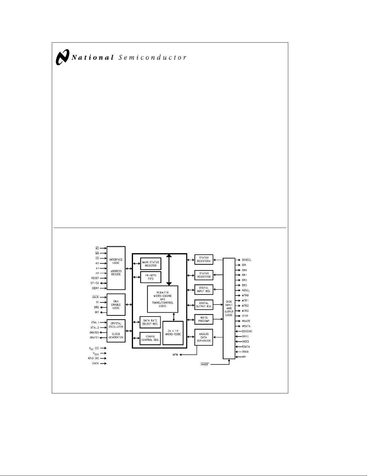
Functional Block Diagram
FIGURE 1-1
SuperFDCTMis a trademark of National Semiconductor Corporation.
TRI-STATE
is a registered trademark of National Semiconductor Corporation.
É
IBM
, PC-ATÉand PS/2Éare registered trademarks of International Business Machines Corp.
É
C
1995 National Semiconductor Corporation RRD-B30M75/Printed in U. S. A.
TL/F/11332
TL/F/11332– 3

Table of Contents
1.0 INTRODUCTION
2.0 PIN DESCRIPTION
3.0 REGISTER DESCRIPTION
3.1 Status Register A (SRA)
3.1.1 SRAÐPS/2 Mode
3.1.2 SRAÐModel 30 Mode
3.2 Status Register B (SRB)
3.2.1 SRBÐPS/2 Mode
3.2.2 SRBÐModel 30 Mode
3.3 Digital Output Register (DOR)
3.4 Tape Drive Register (TDR)
3.5 Main Status Register (MSR)
3.6 Data Rate Select Register (DSR)
3.7 Data Register (FIFO)
3.8 Digital Input Register (DIR)
3.8.1 DIRÐPC-AT Mode
3.8.2 DIRÐPS/2 Mode
3.8.3 DIRÐModel 30 Mode
3.9 Configuration Control Register (CCR)
3.9.1 CCRÐPC-AT and PS/2 Modes
3.9.2 CCRÐModel 30 Mode
3.10 Result Phase Status Registers
3.10.1 Status Register 0 (ST0)
3.10.2 Status Register 1 (ST1)
3.10.3 Status Register 2 (ST2)
3.10.4 Status Register 3 (ST3)
4.0 COMMAND SET DESCRIPTION
4.1 Command Set Summary
4.2 Command Description
4.2.1 Configure Command
4.2.2 Dumpreg Command
4.2.3 Format Command
4.2.4 Invalid Command
4.2.5 Lock Command
4.2.6 Mode Command
4.2.7 NSC Command
4.2.8 Perpendicular Mode Command
4.2.9 Read Data Command
4.2.10 Read Deleted Data Command
4.2.11 Read ID Command
4.2.12 Read A Track Command
4.2.13 Recalibrate Command
4.2.14 Relative Seek Command
4.2.15 Scan Commands
4.2.16 Seek Command
4.2.17 Sense Drive Status Command
4.2.18 Sense Interrupt Command
4.2.19 Set Track Command
4.2.20 Specify Command
4.2.21 Verify Command
4.2.22 Version Command
4.2.23 Write Data Command
4.2.24 Write Deleted Data Command
5.0 FUNCTIONAL DESCRIPTION
5.1 Microprocessor Interface
5.2 Modes of Operation
5.3 Controller Phases
5.3.1 Command Phase
5.3.2 Execution Phase
5.3.2.1 DMA ModeÐFIFO Disabled
5.3.2.2 DMA ModeÐFIFO Enabled
5.3.2.3 Interrupt ModeÐFIFO Disabled
5.3.2.4 Interrupt ModeÐFIFO Enabled
5.3.2.5 Software Polling
5.3.3 Result Phase
5.3.4 Idle Phase
5.3.5 Drive Polling Phase
5.4 Data Separator
5.5 Crystal Oscillator
5.6 Dynamic Window Margin Performance
5.7 Perpendicular Recording Mode
5.8 Data Rate Selection
5.9 Write Precompensation
5.10 Low Power Mode Logic
5.11 Reset Operation
6.0 DEVICE DESCRIPTION
6.1 DC Electrical Characteristics
6.2 AC Electrical Characteristics
6.2.1 AC Test Conditions
6.2.2 Clock Timing
6.2.3 Microprocessor Read Timing
6.2.4 Microprocessor Write Timing
6.2.5 DMA Timing
6.2.6 Reset Timing
6.2.7 Write Data Timing
6.2.8 Drive Control Timing
6.2.9 Read Data Timing
7.0 REFERENCE SECTION
7.1 Mnemonic Definitions for PC8477B Commands
7.2 PC8477B Enhancements vs. 82077AA
7.3 PC8477B Interface in a PC-AT
7.4 Software Initialization Sequence
7.5 PC8477B/PC8477A differences
7.6 Revision History
2

List of Figures
PC8477B Functional Block Diagram АААААААААААААААААААААААААААААААААААААААААААААААААААААААААААААААААААААААААААААА1-1
PC8477B Pin Diagram for 68 Pin PLCC and 60 Pin PQFP АААААААААААААААААААААААААААААААААААААААААААААААААААААААААААА1-2
IBMЙ, Perpendicular, and ISO Formats Supported by Format CommandААААААААААААААААААААААААААААААААААААААААААААААА4-1
PC8477B Data Separator Block Diagram АААААААААААААААААААААААААААААААААААААААААААААААААААААААААААААААААААААААААА5-1
Read Data AlgorithmРState DiagramААААААААААААААААААААААААААААААААААААААААААААААААААААААААААААААААААААААААААААА5-2
PC8477B Dynamic Window Margin Performance ААААААААААААААААААААААААААААААААААААААААААААААААААААААААААААААААААА5-3
g
PC8477B Dynamic Window Margin Performance with
Perpendicular Recording Drive R/W Head and Pre-Erase Head АААААААААААААААААААААААААААААААААААААААААААААААААААААА5-5
Clock Timing АААААААААААААААААААААААААААААААААААААААААААААААААААААААААААААААААААААААААААААААААААААААААААААААААА6-1
Microprocessor Read Timing АААААААААААААААААААААААААААААААААААААААААААААААААААААААААААААААААААААААААААААААААААА6-2
Microprocessor Write Timing АААААААААААААААААААААААААААААААААААААААААААААААААААААААААААААААААААААААААААААААААААА6-3
DMA Timing ААААААААААААААААААААААААААААААААААААААААААААААААААААААААААААААААААААААААААААААААААААААААААААААААААА6-4
Reset Timing АААААААААААААААААААААААААААААААААААААААААААААААААААААААААААААААААААААААААААААААААААААААААААААААААА6-5
Write Data Timing АААААААААААААААААААААААААААААААААААААААААААААААААААААААААААААААААААААААААААААААААААААААААААААА6-6
Drive Control TimingАААААААААААААААААААААААААААААААААААААААААААААААААААААААААААААААААААААААААААААААААААААААААААА6-7
Read Data Timing АААААААААААААААААААААААААААААААААААААААААААААААААААААААААААААААААААААААААААААААААААААААААААААА6-8
PC8477B in a PC-AT System АААААААААААААААААААААААААААААААААААААААААААААААААААААААААААААААААААААААААААААААААААА7-1
PC84777B Initialization ААААААААААААААААААААААААААААААААААААААААААААААААААААААААААААААААААААААААААААААААААААААААА7-2
3% ISVАААААААААААААААААААААААААААААААААААААААААААААААААААААА5-4
List of Tables
Register Description and Addresses АААААААААААААААААААААААААААААААААААААААААААААААААААААААААААААААААААААААААААААА3-1
Drive Enable Values АААААААААААААААААААААААААААААААААААААААААААААААААААААААААААААААААААААААААААААААААААААААААААА3-2
Tape Drive Assignment ValuesААААААААААААААААААААААААААААААААААААААААААААААААААААААААААААААААААААААААААААААААААА3-3
Write Precompensation Delays АААААААААААААААААААААААААААААААААААААААААААААААААААААААААААААААААААААААААААААААААА3-4
Default Precompensation DelaysААААААААААААААААААААААААААААААААААААААААААААААААААААААААААААААААААААААААААААААААА3-5
Data Rate Select Encoding АААААААААААААААААААААААААААААААААААААААААААААААААААААААААААААААААААААААААААААААААААААА3-6
Typical Format Gap Length Values ААААААААААААААААААААААААААААААААААААААААААААААААААААААААААААААААААААААААААААААА4-1
DENSEL Encoding ААААААААААААААААААААААААААААААААААААААААААААААААААААААААААААААААААААААААААААААААААААААААААААА4-2
DENSEL Default Encoding АААААААААААААААААААААААААААААААААААААААААААААААААААААААААААААААААААААААААААААААААААААА4-3
Effects of WGATE and GAP ААААААААААААААААААААААААААААААААААААААААААААААААААААААААААААААААААААААААААААААААААААА4-4
Sector Size Selection ААААААААААААААААААААААААААААААААААААААААААААААААААААААААААААААААААААААААААААААААААААААААААА4-5
SK Effect of Read Data Command ААААААААААААААААААААААААААААААААААААААААААААААААААААААААААААААААААААААААААААААА4-6
Result Phase Termination Values with No Error АААААААААААААААААААААААААААААААААААААААААААААААААААААААААААААААААААА4-7
SK Effect on Read Deleted Data Command ААААААААААААААААААААААААААААААААААААААААААААААААААААААААААААААААААААААА4-8
Maximum Recalibrate Step Pulses Based on R255 and ETR ААААААААААААААААААААААААААААААААААААААААААААААААААААААААА4-9
Scan Command Termination Values ААААААААААААААААААААААААААААААААААААААААААААААААААААААААААААААААААААААААААААА4-10
Status Register 0 Termination Codes АААААААААААААААААААААААААААААААААААААААААААААААААААААААААААААААААААААААААААА4-11
Set Track Register Address АААААААААААААААААААААААААААААААААААААААААААААААААААААААААААААААААААААААААААААААААААА4-12
Step Rate (SRT) Values ААААААААААААААААААААААААААААААААААААААААААААААААААААААААААААААААААААААААААААААААААААААА4-13
Motor Off Time (MFT) Values ААААААААААААААААААААААААААААААААААААААААААААААААААААААААААААААААААААААААААААААААААА4-14
Motor On Time (MNT) ValuesААААААААААААААААААААААААААААААААААААААААААААААААААААААААААААААААААААААААААААААААААА4-15
Verify Command Result Phase Table АААААААААААААААААААААААААААААААААААААААААААААААААААААААААААААААААААААААААААА4-16
Nominal t
Minimum t
PC8477B–82077 Parameter Comparison ААААААААААААААААААААААААААААААААААААААААААААААААААААААААААААААААААААААААА7-1
Density Encoding АААААААААААААААААААААААААААААААААААААААААААААААААААААААААААААААААААААААААААААААААААААААААААААА7-2
Values ААААААААААААААААААААААААААААААААААААААААААААААААААААААААААААААААААААААААААААААААААААААА6-1
ICP,tDRP
ValuesАААААААААААААААААААААААААААААААААААААААААААААААААААААААААААААААААААААААААААААААААААААААААА6-2
WDW
3

1.0 Introduction
The PC8477B advanced floppy disk controller is suitable for
all PC-AT, EISA, PS/2, and general purpose applications.
The operational mode (PC-AT, PS/2, and Model 30) of the
PC8477B is determined by hardware strapping of the IDENT
and MFM pins. DP8473 and Intel 82077AA software compatibility is provided. Key features include the 16 byte FIFO,
PS/2 diagnostic register support, the perpendicular recording mode, CMOS disk interface, and a high performance
analog data separator.
The PC8477B supports the standard PC data rates of 250,
300, 500 kb/s, and 1 Mb/s in MFM encoded data mode, but
is no longer guaranteed through functional testing to support the older FM encoded data mode. References to the
older FM mode remain in this document to clarify the true
functional operation of the device.
The 1 Mb/s data rate is used by new high performance tape
and floppy drives emerging in the PC market today. The new
floppy drives utilize high density media which requires the
PC8477B supported perpendicular recording mode format.
When used with the 1 Mb/s data rate this new format allows
the use of 4 Mb floppy drives which format ED media to
2.88 MB data capacity.
The high performance internal analog data separator needs
no external components. It improves on the window margin
performance standards of the DP8473, and is compatible
with the strict data separator requirements of floppy and
floppy-tape drives.
The PC8477B contains write precompensation and circuitry
that will default to 125 ns for 250, 300, and 500 kb/s,
41.67 ns at 1 Mb/s. These values can be overridden
through software to disable write precompensation or to
provide levels of precompensation up to 250 ns. The
PC8477B has internal 12 mA data bus buffers which allow
direct connection to the system bus. The internal 48 mA
totem-pole disk interface buffers are compatible with both
CMOS drive inputs and 150X resistor terminated disk drive
inputs.
The PC8477B is available in a 68 pin Plastic Leaded Chip
Carrier (PLCC) package, and in a 60 pin Plastic Quad Flat
Package (PQFP).
4
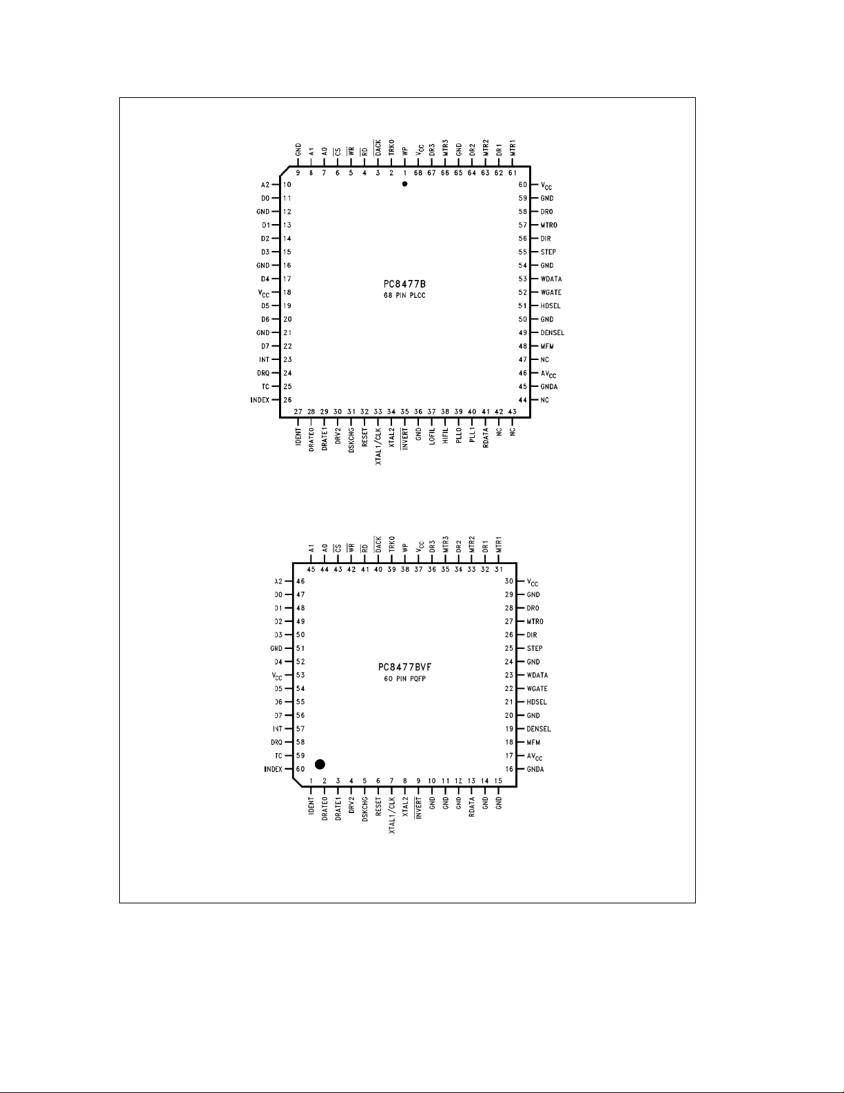
Connection Diagrams
Plastic Chip Carrier (V)
Order Number PC8477BV-1
See NS Package Number V68A
Plastic Quad Flat Package (VF)
Order Number PC8477BVF-1
See NS Package Number VF60A
FIGURE 1-2
TL/F/11332– 1
TL/F/11332– 2
5
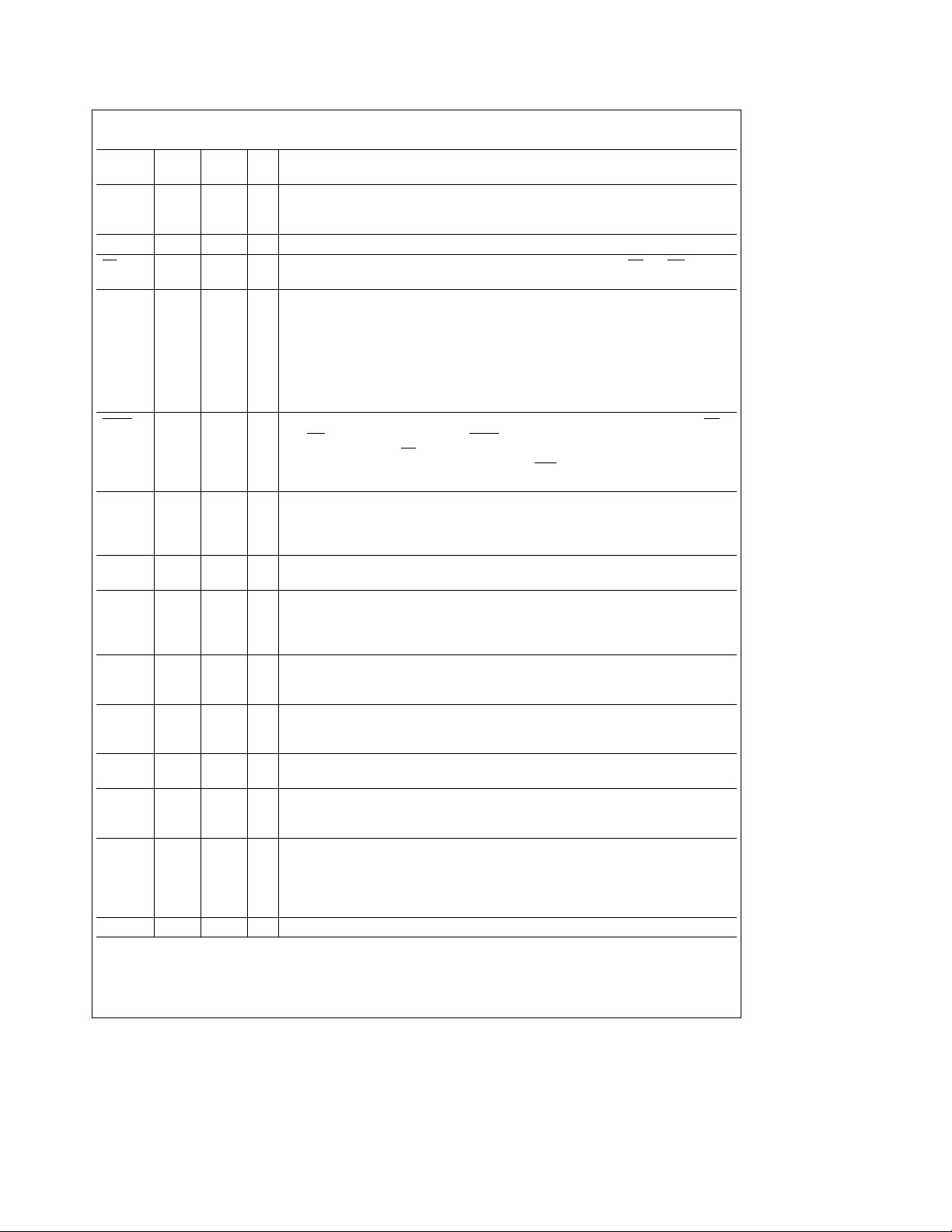
2.0 Pin Description
Symbol
A0 7 44 I Address. These address lines from the microprocessor determine which internal FDC
A1 8 45 register is accessed. See TABLE 3-1 in the Register Description section. A0–A2 are don’t
A2 10 46 cares during a DMA transfer.
AVCC 46 17 Analog Supply. This pin is the 5V supply for the analog data separator.
CS 643IChip Select. Active low input from address decoder used to enable the RD and WR inputs
D0 11 47 I/O Data. Bi-directional data lines to the microprocessor. D0 is the LSB and D7 is the MSB.
D1 13 48 These signals all have 12 mA buffered outputs.
D2 14 49
D3 15 50
D4 17 52
D5 19 54
D6 20 55
D7 22 56
DACK 340IDMA Acknowledge. Active low input to acknowledge the DMA request and enable the RD
DENSEL 49 19 O Density Select. Indicates when a high density data rate (500 kb/s or 1 Mb/s) or a low
DIR 56 26 O Direction. This output determines the direction of the head movement (activeestep in,
DR0 58 28 O Drive Select 0 –3. These are the decoded drive select outputs that are controlled by Digital
DR1 62 32 Output Register bits D0, D1. The Drive Select outputs are gated by DOR bits 4–7.
DR2 64 34
DR3 67 36
DRATE0 28 2 O Data Rate 0,1. These outputs reflect the currently selected data rate, (bits 0 and 1 in the
DRATE1 29 3 CCR or the DSR, whichever was written to last). These pins are totem-pole buffered outputs
DRQ 24 58 O DMA Request. Active high output to signal the DMA controller that a data transfer is needed.
DRV2 30 4 I Drive2. This input indicates whether a second disk drive has been installed. The state of this
DSKCHG 31 5 I Disk Change. The input indicates if the drive door has been opened. The state of this pin is
GND 9, 12, 10, 11, Ground
GNDA 45 16 Analog Ground. This is the analog ground for the data separator.
PLCC PQFP
Pin Pin
16, 21, 12, 14,
36, 50, 15, 20,
54, 59, 24, 29,
65 51
I/O Function
during register I/O. Should be held inactive during DMA transfers.
and WR inputs during a DMA transfer. DACK should be held inactive high during normal read
or write accesses when CS
enabled by bit D3 of the DOR. When in PS/2 mode, DAK
DOR is reserved.
density data rate (250 or 300 kb/s) has been selected. DENSEL is active high for high
density (5.25
IDENT is low. DENSEL is also programmable via the Mode command (see Section 4.2.6).
inactive
(6 mA sink, 4 mA source).
When in PC-AT or Model 30 mode, this signal is enabled by bit D3 of the DOR. When in PS/2
mode, DRQ is always enabled, and bit D3 of the DOR is reserved.
pin is available from Status Register A in PS/2 mode.
available from the Digital Input register. This pin can also be configured as the RGATE data
separator diagnostic input via the Mode command (see Section 4.2.6).
drives) when IDENT is high, and active low for high density (3.5×drives) when
×
e
step out) during a seek operation. During read or writes, DIR will be inactive.
is active. When in PC-AT or Model 30 mode, this signal is
is always enabled, and bit D3 of the
6

2.0 Pin Description (Continued)
Symbol
HDSEL 51 21 O Head Select. This output determines which side of the disk drive is accessed. Active selects side
HIFIL 38 (Note 1) High Filter. No connect. No external capacitor is required. An external capacitor can be
IDENT 27 1 I Identity. During chip reset, the IDENT and MFM pins are sampled to determine the mode of
INDEX 26 60 I Index. This input signals the beginning of a track.
INT 23 57 O Interrupt. Active high output to signal the completion of the execution phase for certain
INVERT 35 9 I Invert. Determines the polarity of all disk interface signals. When tied low, the internal disk output
LOFIL 37 (Note 1) Low Filter. No connect. No external capacitor is required. An external capacitor can be
MFM 48 18 I/O MFM. During a chip reset when in PS/2 mode (IDENT low), this pin is sampled to select the PS/2
MTR0 57 27 O Motor Select 0 – 3. These are the motor enable lines for drives 0– 3, and are controlled by bits D7 –
MTR1 61 31
MTR2 63 33
MTR3 66 35
NC 42 (Note 1) No Connect. These pins must be left unconnected.
PLCC PQFP
Pin Pin
43
44
47
I/O Function
1, inactive selects side 0.
connected, but it will have no effect on the data separator performance.
operation according to the following table:
IDENT MFM Mode
1 1 or NC PC-AT Mode
1 0 Illegal
0 1 or NC PS/2 Mode
0 0 Model 30 Mode
AT ModeÐThe DMA enable bit in the DOR is valid. TC is active high. Status Registers A and B
are disabled (TRI-STATEÉ).
Model 30 ModeÐThe DMA enable bit in the DOR is valid. TC is active high. Status Registers A
and B are enabled.
PS/2 ModeÐThe DMA enable bit in the DOR is a don’t care, and the DRQ and INT signals will
always be enabled. TC is active low. Status Registers A and B are enabled.
After chip reset, the state of IDENT determines the polarity of the DENSEL output.
When IDENT is a logic ‘‘1’’, DENSEL is active high for 500 kb/s and 1 Mb/s data rates.
When IDENT is a logic ‘‘0’’, DENSEL is active low for 500 kb/s and 1 Mb/s data rates.
(See Mode command for further explanation of DENSEL.)
commands. Also used to signal when a data transfer is ready during a Non-DMA operation. When
in PC-AT or Model 30 mode, this signal is enabled by bit D3 of the DOR. When in PS/2 mode, INT
is always enabled, and bit D3 of the DOR is reserved.
buffers and inverting Schmitt input receivers are enabled, and the disk interface signals are active
low. When tied high, the disk interface signals are active high, and external receivers and output
buffers are required.
connected, but it will have no effect on the data separator performance.
mode (MFM high), or the Model 30 mode (MFM low). An internal pull-up or external pull-down
10 kX resistor will select between the two PS/2 modes. When the PC-AT mode is desired (IDENT
high), MFM should be left pulled high internally. MFM reflects the current data encoding format
when RESET is inactive. MFM
can also be configured as the PUMP data separator diagnostic output via the Mode command (see
Section 4.2.6).
D4 of the Digital Output register.
e
high, FMelow. Defaults to low after a chip reset. This signal
7
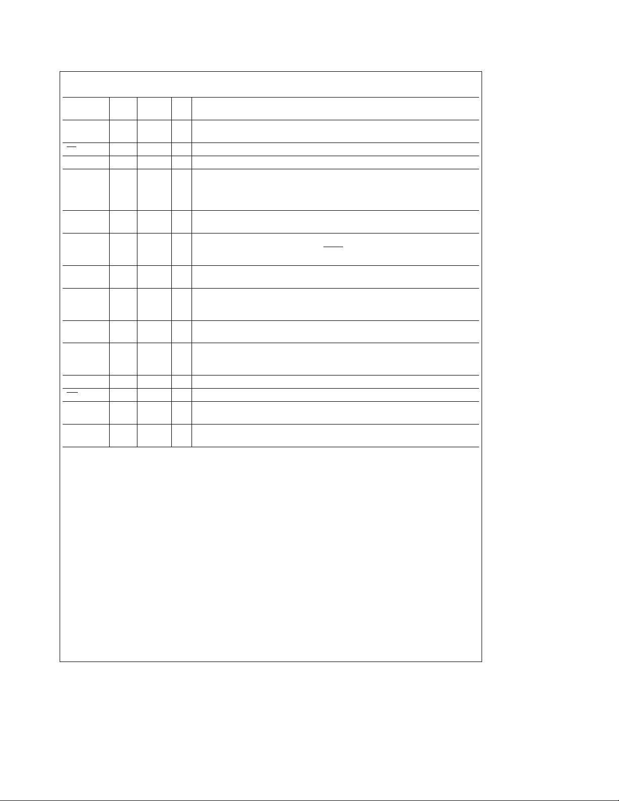
2.0 Pin Description (Continued)
Symbol
PLL0 39 (Note 1) Phase Locked Loop 0,1. No connects. These pins can be tied high or low with no affect
PLL1 40 on the data separator performance.
RD 441IRead. Active low input to signal a read from the controller to the microprocessor.
RDATA 41 13 I Read Data. This input is the raw serial data read from the disk drive.
RESET 32 6 I Reset. Active high input that resets the controller to the idle state, and resets all disk
STEP 55 25 O Step. This output signal issues pulses to the disk drive at a software programmable rate
TC 25 59 I Terminal Count. Control signal from the DMA controller to indicate the termination of a
TRK0 2 39 I Track 0. This input indicates to the controller that the head of the selected disk drive is at
V
CC
WDATA 53 23 O Write Data. This output is the write precompensated serial data that is written to the
WGATE 52 22 O Write Gate. This output signal enables the write circuitry of the selected disk drive.
WP 1 38 I Write Protect. This input indicates that the disk in the selected drive is write protected.
WR 542IWrite. Active low input to signal a write from the microprocessor to the controller.
XTAL1/CLK 33 7 I Crystal1/Clock. One side of an external 24 MHz crystal is attached here. If a crystal is
XTAL2 34 8 I Crystal2. One side of an external 24 MHz crystal is attached here. This pin is left
Note 1: When converting the 68 pin PLCC to a 60 pin PQFP, eight pins were removed. The following signals were affected in this conversion process:
PLCC PQFP
Pin Pin
I/O Function
interface outputs to their inactive states. The DOR, DSR, CCR, Mode command,
Configure command, and Lock command parameters are cleared to their default values.
The Specify command parameters are not affected.
to move the head during a seek operation.
DMA transfer. TC is accepted only when DACK
is active. TC is active high in PC-AT and
Model 30 modes, and active low in PS/2 mode.
track zero.
18 30 Voltage. This is thea5V supply voltage for the digital circuitry.
60 37
68 53
selected disk drive. Precompensation is software selectable.
WGATE has been designed to prevent glitches during power up and power down. This
prevents writing to the disk when power is cycled.
not used, a TTL or CMOS compatible clock is connected to this pin.
unconnected if an external clock is used.
1. NC (No Connect) signals on pins 42 and 43 of the 68 pin PLCC were converted to GND (Ground) signals on pins 14 and 15 of the 60 pin PQFP,
respectively.
2. NC (No Connect) signals on pins 44 and 47 of the 68 pin PLCC were removed for the 60 pin PQFP.
3. HIFIL (pin 38) and LOFIL (pin 37) of the 68 pin PLCC were removed for the 60 pin PQFP.
4. PLL0 (pin 39) and PLL1 (pin 40) of the 68 PLCC were converted to GND (ground) signals on the PQFP (pins 11 and 12 respectively).
5. The GND (ground) signals on pins 9, 12, 21, and 65 of the 68 pin PLCC are not available for the 60 pin PQFP. These signals are tied to ground internally.
8
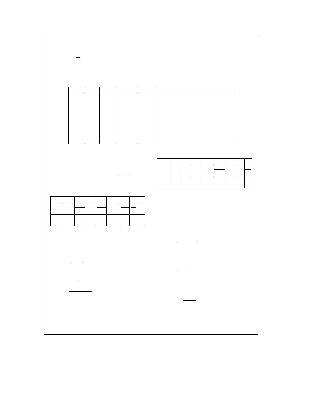
3.0 Register Description
The following PC8477B registers are mapped into the addresses shown below, with the base address range being
provided by the CS
diskette controller primary address range is 3F0 to 3F7
(hex), and the secondary address range is 370 to 377 (hex).
The PC8477B supports three different register modes: the
3.1 STATUS REGISTER A (SRA) Read Only
This is a read only diagnostic register that is part of the
PS/2 floppy controller register set, and is enabled when in
the PS/2 or Model 30 mode. This register monitors the state
of the INT pin and some of the disk interface signals. The
state of these bits is independent of the INVERT
SRA can be read at any time when in PS/2 mode. In the
PC-AT mode, D7 – D0 are TRI-STATE during a mP read.
3.1.1 SRAÐPS/2 Mode
INT
DESC
PEND
RESET
COND
D7 Interrupt Pending: This active high bit reflects
D6 2nd Drive Installed
D5 Step: Active high status of the STEP disk inter-
D4 Track 0
D3 Head Select: Active high status of the HDSEL
D2 Index
D1 Write Protect
D0 Direction: Active high status of the DIR disk in-
pin. For PC-AT or PS/2 applications, the
TABLE 3-1. Register Description and Addresses
A2 A1 A0 IDENT R/W Register
0 0 0 0 R Status Register A SRA
0 0 1 0 R Status Register B SRB
0 1 0 X R/W Digital Output Register DOR
0 1 1 X R/W Tape Drive Register TDR
1 0 0 X R Main Status Register MSR
1 0 0 X W Data Rate Select Register DSR
1 0 1 X R/W Data Register (FIFO) FIFO
1 1 0 X X None (Bus TRI-STATE)
1 1 1 X R Digital Input Register DIR
1 1 1 X W Configuration Control Register CCR
Note: SRA and SRB are enabled by IDENTe0 during a chip reset only.
pin. The
D7 D6 D5 D4 D3 D2 D1 D0
DRV2 STEP TRK0 HDSEL INDX WP DIR
0 N/A 0 N/A 0 N/A N/A 0
the state of the INT pin.
: Active low status of the
DRV2 disk interface input, indicating if a second
drive has been installed.
face output.
: Active low status of the TRK0 disk in-
terface input.
disk interface output.
: Active low status of the INDEX disk in-
terface input.
: Active low status of the WP disk
interface input.
terface output.
PC-AT mode, PS/2 mode (Models 50/60/80), and the Model 30 mode (Model 30). See Section 5.1 for more details on
how each register mode is enabled. When applicable, the
register definition for each mode of operation will be given.
If no special notes are made, then the register is valid for all
three register modes.
3.1.2 SRAÐ Model 30 Mode
D7 D6 D5 D4 D3 D2 D1 D0
INT
DESC
RESET
COND
D7 Interrupt Pending: This active high bit reflects
D6 DMA Request: Active high status of the DRQ
D5 Step: Active high status of the latched STEP
D4 Track 0: Active high status of TRK0 disk inter-
D3 Head Select
D2 Index: Active high status of the INDEX disk in-
D1 Write Protect: Active high status of the WP
D0 Direction
3.2 STATUS REGISTER B (SRB) Read Only
This is a read only diagnostic register that is part of the
PS/2 floppy controller register set, and is enabled when in
the PS/2 or Model 30 mode. The state of these bits is independent of the INVERT
time when in PS/2 mode. In the PC-AT mode, D7–D0 are
TRI-STATE during a mP read.
DRQ STEP TRK0 HDSEL INDX WP DIR
PEND
0 0 0 N/A 1 N/A N/A 1
that state of the INT pin.
signal.
disk interface output. This bit is latched with the
STEP output going active, and is cleared with a
read from the DIR, or with a hardware or software reset.
face input.
disk interface output.
terface input.
disk interface input.
terface output.
: Active low status of the HDSEL
: Active low status of the DIR disk in-
pin. The SRB can be read at any
9
3.0 Register Description (Continued)
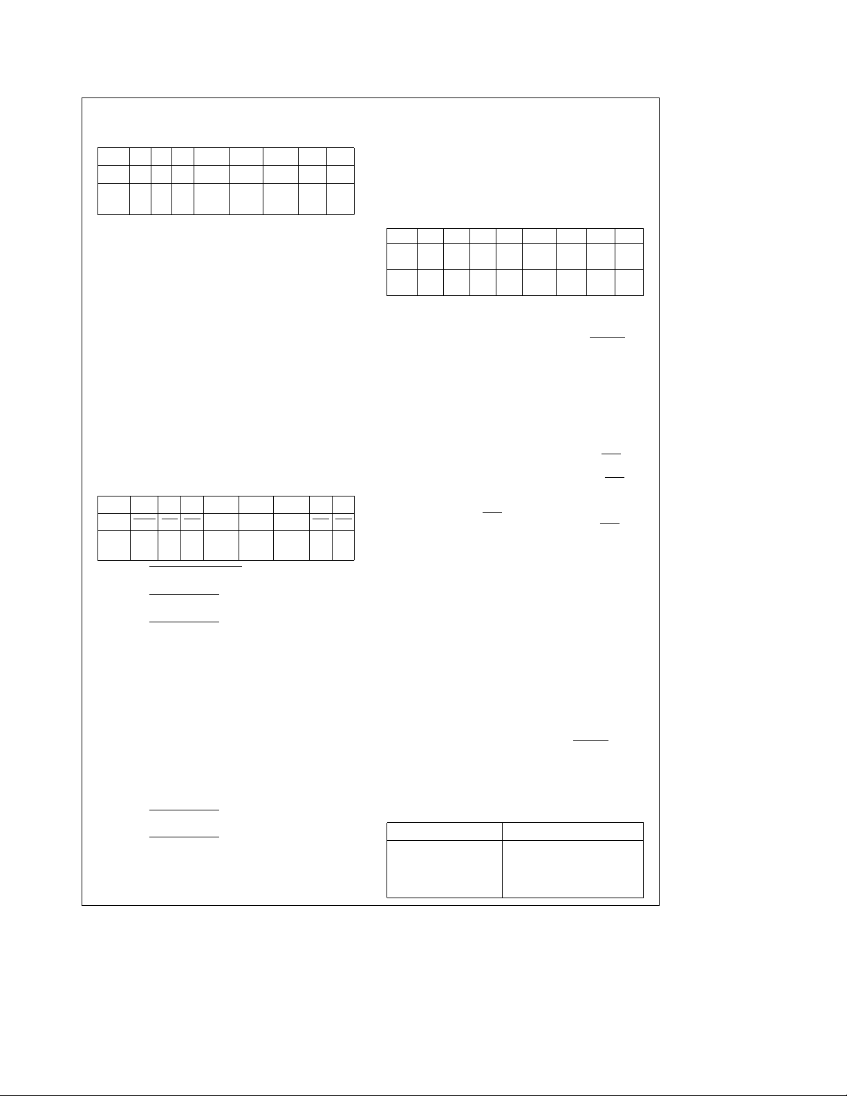
3.2.1 SRBÐPS/2 Mode
D7 D6 D5 D4 D3 D2 D1 D0
DESC 1 1 DR0 WDATA RDATA WGATE MTR1 MTR0
RESET
N/A N/A 0 0 0 0 0 0
COND
D7 Reserved: Always 1.
D6 Reserved: Always 1.
D5 Drive Select 0: Reflects the status of the Drive
D4 Write Data: Every inactive edge transition of
D3 Read Data: Every positive edge transition of the
D2 Write Gate: Active high status of the WGATE
D1 Motor Enable 1: Active high status of the
D0 Motor Enable 0: Active high status of the
3.2.2 SRBÐModel 30 Mode
DESC DRV2 DR1 DR0 WDATA RDATA WGATE DR3 DR2
RESET
COND
D7 2nd Drive Installed: Active low status of the
D6 Drive Select 1
D5 Drive Select 0
D4 Write Data: Active high status of latched
D3 Read Data: Active high status of latched
D2 Write Gate: Active high status of latched
D1 Drive Select 3
D0 Drive Select 2
Select 0 bit in the DOR (address 2, bit 0). This
bit is cleared after a hardware reset, not a software reset.
the WDATA disk interface output causes this bit
to change states.
RDATA disk interface output causes this bit to
change states.
disk interface output.
MTR1 disk interface output. Low after a hardware reset, unaffected by a software reset.
MTR0 disk interface output. Low after a hardware reset, unaffected by a software reset.
D7 D6 D5 D4 D3 D2 D1 D0
N/A 1 1 0 0 0 1 1
DRV2 disk interface input.
: Active low status of the DR1
disk interface output.
: Active low status of the DR0
disk interface output.
WDATA signal. This bit is latched by the inactive going edge of WDATA and is cleared by a
read from the DIR. This bit is not gated by
WGATE.
RDATA signal. This bit is latched by the inactive
going edge of RDATA and is cleared by a read
from the DIR.
WGATE signal. This bit is latched by the active
going edge of WGATE and is cleared by a read
from the DIR.
: Active low status of the DR3
disk interface output.
: Active low status of the DR2
disk interface output.
3.3 DIGITAL OUTPUT REGISTER (DOR) Read/Write
The DOR controls the drive select and motor enable disk
interface outputs, enables the DMA logic, and contains a
software reset bit. The contents of the DOR are set to 00
(hex) after a hardware reset, and are unaffected by a software reset. The DOR can be written to at any time.
DOR
D7 D6 D5 D4 D3 D2 D1 D0
DESC MTR3 MTR2 MTR1 MTR0 DMAEN RESET
RESET
0000 0 0 0 0
COND
DRIVE DRIVE
SEL 1 SEL 0
D7 Motor Enable 3: This bit controls the MTR3
disk interface output.A1inthis bit causes the
MTR3 pin to go active. The actual level of
MTR3 depends on the state of the INVERT
pin.
D6 Motor Enable 2: Same function as D7 except
for MTR2.
D5 Motor Enable 1: Same function as D7 except
for MTR1.
D4 Motor Enable 0: Same function as D7 except
for MTR0.
D3 DMA Enable: This bit has two modes of opera-
tion. PC-AT mode or Model 30 mode: Writing
a 1 to this bit will enable the DRQ, DAK
, INT
and TC pins. Writinga0tothis bit will
TRI-STATE DRQ and INT, and disable DAK
and
TC. This bit is a 0 after a reset when in these
modes. PS/2 mode: This bit is reserved, and
the DRQ, DAK
enabled. During a reset, the DRQ, DAK
, INT and TC pins will always be
, and
INT lines will remain enabled, and D3 will be a
0.
D2 Reset Controller: Writinga0tothis bit resets
the controller. It will remain in the reset condition untila1iswritten to this bit. A software
reset does not affect the DSR, CCR, and other
bits of the DOR. A software reset will affect the
Configure and Mode command bits (see Section 4.0 Command Set Description). The minimum time that this bit must be low is 100 ns.
Thus, toggling the Reset Controller bit during
consecutive writes to the DOR is an acceptable
method of issuing a software reset.
D1–D0 Drive Select: These two bits are binary encod-
ed for the four drive selects DR0 –DR3, so that
only one drive select output is active at a time.
The actual level of the drive select outputs is
determined by the state of the INVERT
pin.
It is common programming practice to enable both the motor enable and drive select outputs for a particular drive.
Table 3-2 below shows the DOR values to enable each of
the four drives.
TABLE 3-2. Drive Enable Values
Drive DOR Value
0 1C (Hex)
12D
24E
38F
10

3.0 Register Description (Continued)
3.4 DRIVE REGISTER (TDR) Read/Write
This register is used to assign a particular drive number with
the tape drive support mode of the data separator. All other
logical drives are assigned floppy drive support with the
data separator. Any future reference to the assigned tape
drive will invoke tape drive support. The TDR is unaffected
by a software reset.
TDR
D7 D6 D5 D4 D3 D2 D1 D0
DESC XXXXXX
RESET
N/A N/A N/A N/A N/A N/A 0 0
COND
D7–D2 Reserved: These bits are ignored when written
to and are TRI-STATE when read.
D1–D0 Tape Select 1,0: These two bits assign a logical
drive number to be a tape drive. Drive 0 is not
available as a tape drive, and is reserved as the
floppy disk boot drive. See Table 3-3 for the
tape drive assignment values.
TABLE 3-3. Tape Drive Assignment Values
TAPESEL1 TAPESEL0
0 0 None
011
102
113
3.5 MAIN STATUS REGISTER (MSR) Read Only
The read only Main Status Register indicates the current
status of the disk controller. The Main Status Register is
always available to be read. One of its functions is to control
the flow of data to and from the Data Register (FIFO). The
Main Status Register indicates when the disk controller is
ready to send or receive data through the Data Register. It
should be read before each byte is transferred to or from
the Data Register except during a DMA transfer. No delay is
required when reading this register after a data transfer.
After a hardware or software reset, or recovery from a power down state, the Main Status Register is immediately available to be read by the mP. It will contain a value of 00 hex
until the oscillator circuit has stabilized, and the internal registers have been initialized. When the PC8477B is ready to
receive a new command, it will report an 80 hex to the mP.
The system software can poll the MSR until it is ready. The
worst case time allowed for the MSR to report an 80 hex
value (RQM set) is 2.5 ms after reset or power up.
MSR
D7 D6 D5 D4 D3 D2 D1 D0
RQM DIO NON CMD DRV3 DRV2 DRV1 DRV0
DESC
RESET
COND
DMA PROG BUSY BUSY BUSY BUSY
00000000
TAPE TAPE
SEL1 SEL0
DRIVE
SELECTED
D7 Request for Master: Indicates that the control-
ler is ready to send or receive data from the mP
through the FIFO. This bit is cleared immediately after a byte transfer and will become set
again as soon as the disk controller is ready for
the next byte. During a Non-DMA Execution
phase, the RQM indicates the status of the interrupt pin.
D6 Data I/O (Direction): Indicates whether the
controller is expecting a byte to be written to (0)
or read from (1) the Data Register.
D5 Non-DMA Execution: Indicates that the con-
troller is in the Execution Phase of a byte transfer operation in the Non-DMA mode. Used for
multiple byte transfers by the mP in the Execution Phase through interrupts or software polling.
D4 Command in Progress: This bit is set after the
first byte of the Command Phase is written. This
bit is cleared after the last byte of the Result
Phase is read. If there is no Result Phase in a
command, the bit is cleared after the last byte
of the Command Phase is written.
D3 Drive 3 Busy: Set after the last byte of the
Command Phase of a Seek or Recalibrate command is issued for drive 3. Cleared after reading
the first byte in the Result Phase of the Sense
Interrupt Command for this drive.
D2 Drive 2 Busy: Same as above for drive 2.
D1 Drive 1 Busy: Same as above for drive 1.
D0 Drive 0 Busy: Same as above for drive 0.
3.6 DATA RATE SELECT REGISTER (DSR) Write Only
This write only register is used to program the data rate,
amount of write precompensation, power down mode, and
software reset. The data rate is programmed via the CCR,
not the DSR, for PC-AT and PS/2 Model 30 and MicroChannel applications. Other applications can set the data rate in
the DSR. The data rate of the floppy controller is determined by the most recent write to either the DSR or CCR.
The DSR is unaffected by a software reset. A hardware reset will set the DSR to 02 (hex), which corresponds to the
default precompensation setting and 250 kb/s.
DSR
D7 D6 D5 D4 D3 D2 D1 D0
S/W LOW0PRE- PRE- PRE-
DESC
RESET PWR COMP2 COMP1 COMP0
RESET
000000 1 0
COND
DRATE1 DRATE0
D7 Software Reset: A 1 in this bit location will re-
set the part similar to the DOR RESET (D2) except that this software reset is self-clearing.
D6 Low Power: A 1 to this bit will put the controller
into the Manual Low Power mode. The oscillator and data separator circuits will be turned off.
Manual Low Power can also be accessed via
the Mode command. The chip will come out of
low power after a software reset, or access to
the Data Register or Main Status Register.
11

3.0 Register Description (Continued)
D5 Undefined: Should be set to 0.
D4–D2 Precompensation Select: These three bits se-
D1–D0 Data Rate Select 1,0: These bits determine the
Note: FM mode is not guaranteed through functional testing.
3.7 DATA REGISTER (FIFO) Read/Write
The FIFO (read/write) is used to transfer all commands,
data, and status between the mP and the PC8477B. During
the Command Phase, the mP writes the command bytes into
the FIFO after polling the RQM and DIO bits in the MSR.
During the Result Phase, the mP reads the result bytes from
the FIFO after polling the RQM and DIO bits in the MSR.
The enabling of the FIFO and setting of the FIFO threshold
is done via the Configure command. If the FIFO is enabled,
lect the amount of write precompensation the
floppy controller will use on the WDATA disk
interface output. Table 3-4 shows the amount of
precompensation used for each bit pattern. In
most cases, the default values (Table 3-5) can
be used; however, alternate values can be chosen for specific types of drives and media.
Track 0 is the default starting track number for
precompensation. The starting track number
can be changed in the Configure command.
data rate for the floppy controller. See Table 3-6
for the corresponding data rate for each value
of D1, D0. The data rate select bits are unaffected by a software reset, and are set to 250 kb/s
after a hardware reset.
TABLE 3-4. Write Precompensation Delays
PRECOMP
432
Precompensation Delay
1 1 1 0.0 ns
0 0 1 41.7 ns
0 1 0 83.3 ns
0 1 1 125.0 ns
1 0 0 166.7 ns
1 0 1 208.3 ns
1 1 0 250.0 ns
0 0 0 DEFAULT
TABLE 3-5. Default Precompensation Delays
Data Rate Precompensation Delay
1 Mb/s 41.7 ns
500 kb/s 125.0 ns
300 kb/s 125.0 ns
250 kb/s 125.0 ns
TABLE 3-6. Data Rate Select Encoding
Data Rate Select Data Rate
1 2 MFM FM
1 1 1 Mb/s Illegal
0 0 500 kb/s 250 kb/s
0 1 300 kb/s 150 kb/s
1 0 250 kb/s 125 kb/s
only the Execution Phase byte transfers use the 16 byte
FIFO. The FIFO is always disabled during the Command
and Result Phases of a controller operation. If the FIFO is
enabled, it will not be disabled after a software reset if the
LOCK bit is set in the Lock Command. After a hardware
reset, the FIFO is disabled to maintain compatibility with PCAT systems.
The 16 byte FIFO can be used for DMA, Interrupt, or software polling type transfers during the execution of a read,
write, format, or scan command. In addition, the FIFO can
be put into a Burst or Non-Burst mode with the Mode command. In the Burst mode, DRQ or INT remains active until
all of the bytes have been transferred to or from the FIFO. In
the Non-Burst mode, DRQ or INT is deasserted for 350 ns
to allow higher priority transfer requests to be serviced. The
Mode command can also disable the FIFO for either reads
or writes separately. The FIFO allows the system a larger
latency without causing a disk overrun/underrun error. Typical uses of the FIFO would be at the 1 Mb/s data rate, or
with multi-tasking operating systems. The default state of
the FIFO is disabled, with a threshold of zero. The default
state is entered after a hardware reset.
Data Register (FIFO)
D7 D6 D5 D4 D3 D2 D1 D0
DESC Data[7:0
RESET
COND
]
Byte Mode
During the Execution Phase of a command involving data
transfer to/from the FIFO, the system must respond to a
data transfer service request based on the following formula:
Maximum Allowable Data Transfer Service Time
(THRESH
a
1)c8ct
DRP
b
(16ct
ICP
)
This formula is good for all data rates with the FIFO enabled
or disabled. THRESH is a four bit value programmed in the
Configure command, which sets the FIFO threshold. If the
FIFO is disabled, THRESH is zero in the above formula. The
last term of the formula, (16
to the microcode overhead required by the PC8477B. This
c
t
) is an inherent delay due
ICP
delay is also data rate dependent. See Table 6-1 for the
t
and t
DRP
ICP
times.
The programmable FIFO threshold (THRESH) is useful in
adjusting the floppy controller to the speed of the system. In
other words, a slow system with a sluggish DMA transfer
capability would use a high value of THRESH, giving the
system more time to respond to a data transfer service request (DRQ for DMA mode or INT for Interrupt mode). Conversely, a fast system with quick response to a data transfer
service request would use a low value of THRESH.
3.8 DIGITAL INPUT REGISTER (DIR) Read Only
This diagnostic register is used to detect the state of the
DSKCHG disk interface input and some diagnostic signals.
The function of this register depends on the register mode
of operation. When in the PC-AT mode, the D6 – D0 are
TRI-STATE to avoid conflict with the fixed disk status register at the same address. The DIR is unaffected by a software reset.
12
3.0 Register Description (Continued)
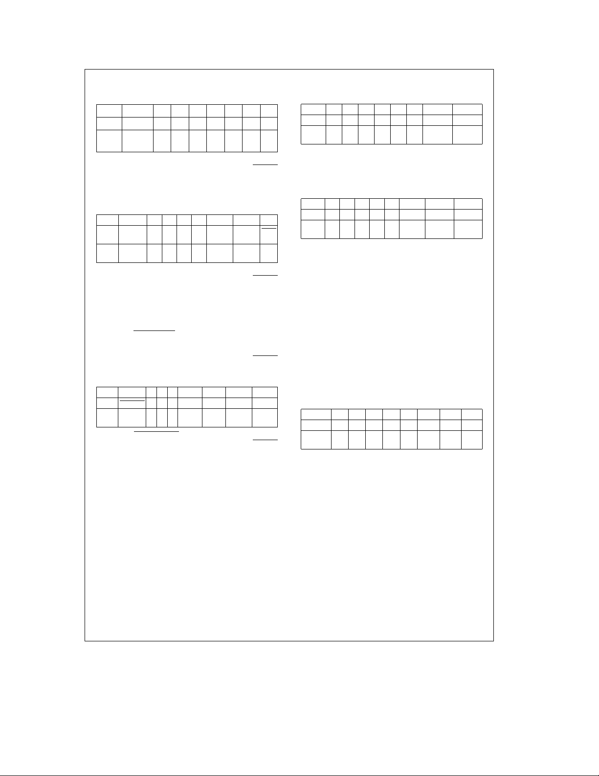
3.8.1 DIRÐPC-AT Mode
D7 D6 D5 D4 D3 D2 D1 D0
DESC DSKCHG X X X X X X X
RESET
COND
D7 Disk Changed: Active high status of DSKCHG
D6–D0 Undefined: TRI-STATE. Used by hard disk con-
3.8.2 DIRÐPS/2 Mode
DESC DSKCHG 1 1 1 1 DRATE1 DRATE0
RESET
COND
D7 Disk Changed: Active high status of DSKCHG
D6–D3 Reserved: Always 1.
D2–D1 Data Rate Select 1,0: These bits indicate the
D0 High Density
3.8.3 DIRÐModel 30 Mode
DESC DSKCHG 0 0 0 DMAEN NOPRE DRATE1 DRATE0
RESET
COND
D7 Disk Changed: Active low status of DSKCHG
D6–D4 Reserved: Always 0.
D3 DMA Enable: Active high status of the DMAEN
D2 No Precompensation: Active high status of the
D1–D0 Data Rate Select 1,0: These bits indicate the
3.9 CONFIGURATION CONTROL REGISTER (CCR) Write
Only
This is the write only data rate register commonly used in
PC-AT applications. This register is not affected by a software reset, and is set to 250 kb/s after a hardware reset.
The data rate of the floppy controller is determined by the
last write to either the CCR or DSR.
N/A N/A N/A N/A N/A N/A N/A N/A
disk interface input, independent of INVERT
value.
troller status register.
D7 D6 D5 D4 D3 D2 D1 D0
N/A N/A N/A N/A N/A N/A N/A 1
disk interface input, independent of INVERT
value.
status of the DRATE1 – 0 bits programmed
through the DSR/CCR.
: This bit is low when the 1 Mb/s
or 500 kb/s data rate is chosen, and high when
the 300 kb/s or 250 kb/s data rate is chosen.
This bit is independent of the IDENT or INVERT
value.
D7 D6 D5 D4 D3 D2 D1 D0
N/A 0 0 0 0 0 1 0
disk interface input, independent of INVERT
value.
bit in the DOR.
NOPRE bit in the CCR.
status of the DRATE1 – 0 bits programmed
through the DSR/CCR.
HIGH
DEN
3.9.1 CCRÐPC-AT and PS/2 Modes
D7 D6 D5 D4 D3 D2 D1 D0
DESC 0 0 0 0 0 0 DRATE1 DRATE0
RESET
N/A N/A N/A N/A N/A N/A 1 0
COND
D7–D2 Reserved: Should be set to 0.
D1–D0 Data Rate Select 1,0: These bits determine the
data rate of the floppy controller. See Table 3-6
for the appropriate values.
3.9.2 CCRÐModel 30 Mode
D7 D6 D5 D4 D3 D2 D1 D0
DESC 0 0 0 0 0 NOPRE DRATE1 DRATE0
RESET
N/A N/A N/A N/A N/A 0 1 0
COND
D7–D3 Reserved: Should be set to 0.
D2 No Precompensation: This bit can be set by
software, but it has no functionality. It can be
read by bit D2 of the DIR when in the Model 30
register mode. Unaffected by a software reset.
D1–D0 Data Rate Select 1,0: These bits determine the
data rate of the floppy controller. See Table 3-6
for the appropriate values.
3.10 RESULT PHASE STATUS REGISTERS
The Result Phase of a command contains bytes that hold
status information. The format of these bytes are described
below. Do not confuse these status bytes with the Main
Status Register, which is a read only register that is always
valid. The Result Phase status registers are read from the
Data Register (FIFO) only during the Result Phase of certain
commands (see Section 4.1 Command Set Summary). The
status of each register bit is indicated when the bit is a 1.
3.10.1 Status Register 0 (ST0)
D7 D6 D5 D4 D3 D2 D1 D0
DESC IC IC SE EC 0 HDS DS1 DS0
RESET
COND
00000 0 0 0
D7–D6 Interrupt Code:
e
00
Normal Termination of Command.
e
01
Abnormal Termination of Command. Execution of command was started, but was
not successfully completed.
e
10
Invalid Command Issued. Command issued was not recognized as a valid command.
e
11
Internal drive ready status changed state
during the drive polling mode. Only occurs
after a hardware or software reset.
D5 Seek End: Seek, Relative Seek, or Recalibrate
command completed by the controller. (Used
during a Sense Interrupt command.)
D4 Equipment Check: After a Recalibrate com-
mand, Track 0 signal failed to occur. (Used during Sense Interrupt command.)
D3 Not Used. Always 0.
13
3.0 Register Description (Continued)
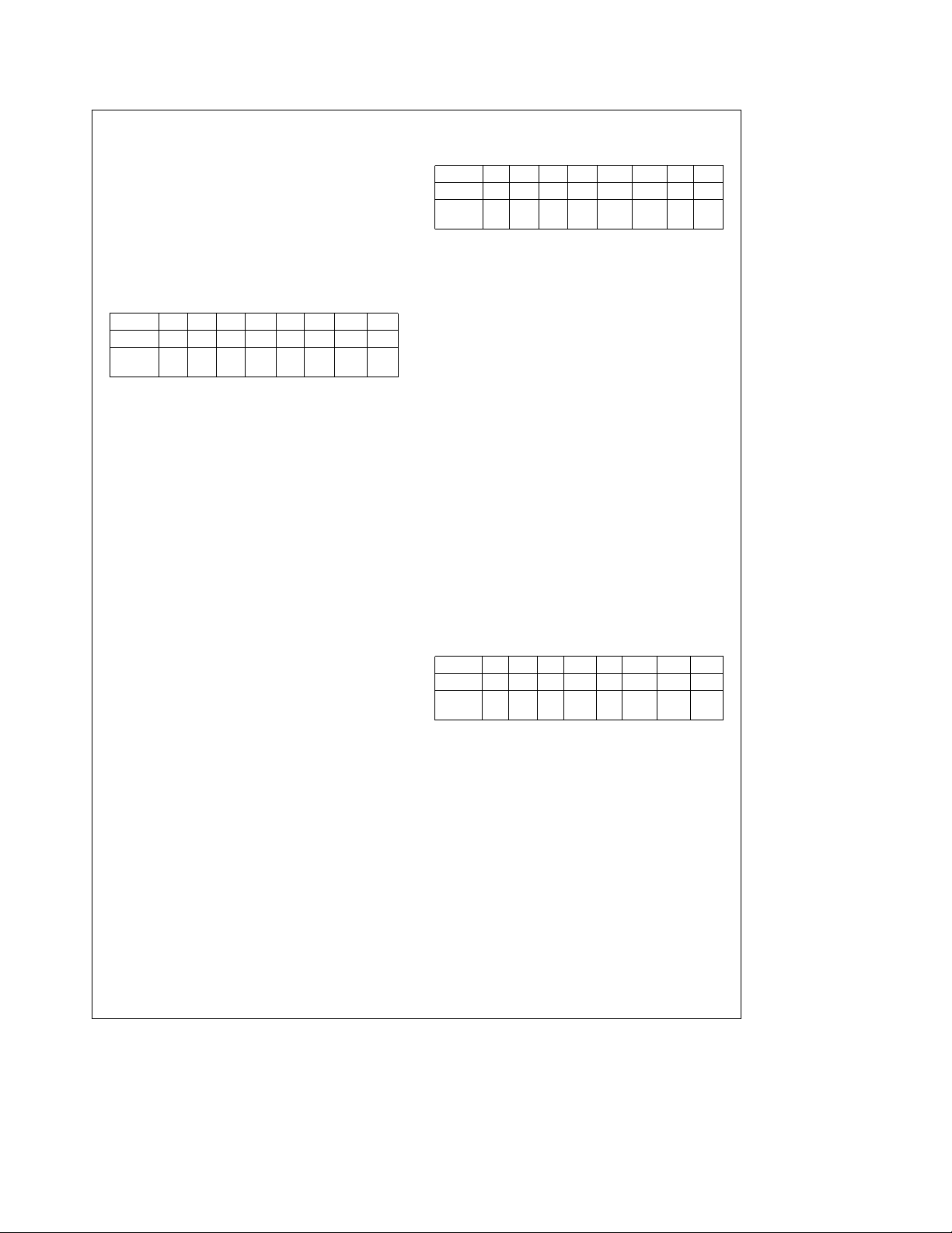
D2 Head Select: Indicates the active high status of
D1–D0 Drive Select 1,0: These two binary encoded
3.10.2 Status Register 1 (ST1)
DESC ET 0 CE OR 0 ND NW MA
RESET
COND
D7 End of Track: Controller transferred the last
D6 Not Used. Always 0.
D5 CRC Error: If this bit is set and bit 5 of ST2 is
D4 Overrun: Controller was not serviced by the mP
D3 Not Used. Always 0.
D2 No Data: Three possible problems:
D1 Not Writable: Write Protect pin is active when a
D0 Missing Address Mark: If bit 0 of ST2 is clear
the HDSEL pin at the end of the Execution
Phase.
bits indicate the logical drive selected at the end
of the Execution Phase.
e
00
Drive 0 selected.
e
01
Drive 1 selected.
e
10
Drive 2 selected.
e
11
Drive 3 selected.
D7 D6 D5 D4 D3 D2 D1 D0
000 0 00 0 0
byte of the last sector without the TC pin becoming active. The last sector is the End of
Track sector number programmed in the Command Phase.
clear, then there was a CRC error in the Address Field of the correct sector. If bit 5 of ST2
is also set, then there was a CRC error in the
Data Field.
soon enough during a data transfer in the Execution Phase. For read operations, indicates a
data overrun. For write operations, indicates a
data underrun.
1. Controller cannot find the sector specified in
the Command Phase during the execution of
a Read, Write, Scan, or Verify command. An
address mark was found however, so it is not
a blank disk.
2. Controller cannot read any Address Fields
without a CRC error during a Read ID command.
3. Controller cannot find starting sector during
execution of Read A Track command.
Write or Format command is issued.
then the controller cannot detect any Address
Field Address Mark after two disk revolutions. If
bit 0 of ST2 is set then the controller cannot
detect the Data Field Address Mark after finding
the correct Address Field.
3.10.3 Status Register 2 (ST2)
D7 D6 D5 D4 D3 D2 D1 D0
DESC 0 CM CD WT SEH SNS BT MD
RESET
COND
D7 Not Used. Always 0.
D6 Control Mark: Controller tried to read a sector
D5 CRC Error in Data Field: Controller detected a
D4 Wrong Track: Only set if desired sector is not
D3 Scan Equal Hit: ‘‘Equal’’ condition satisfied dur-
D2 Scan Not Satisfied: Controller cannot find a
D1 Bad Track: Only set if the desired sector is not
D0 Missing Address Mark in Data Field: Control-
3.10.4 Status Register 3 (ST3)
DESC 0 WP 1 TK0 1 HDS DS1 DS0
RESET
COND
D7 Not Used. Always 0.
D6 Write Protect: Indicates active high status of
D5 Not Used. Always 1.
D4 Track 0: Indicates active high status of the
D3 Not Used. Always 1.
D2 Head Select: Indicates the active high status of
D1–D0 Drive Select 1,0: These two binary encoded
0000 0 0 00
which contained a deleted data address mark
during execution of Read Data or Scan commands. Or, if a Read Deleted Data command
was executed, a regular address mark was detected.
CRC error in the Data Field. Bit 5 of ST1 is also
set.
found, and the track number recorded on any
sector of the current track is different from the
track address specified in the Command Phase.
ing any Scan command.
sector on the track which meets the desired
condition during any Scan command.
found, the track number recorded on any sector
on the track is FF (hex) indicating a hard error in
IBM format, and is different from the track address specified in the Command Phase.
ler cannot find the Data Field AM during a Read,
Scan, or Verify command. Bit 0 of ST1 is also
set.
D7 D6 D5 D4 D3 D2 D1 D0
00101 0 0 0
the WP pin.
TRK0 pin.
the HD bit in the Command Phase.
bits indicate the DS1 –DS0 bits in the Command
Phase.
14
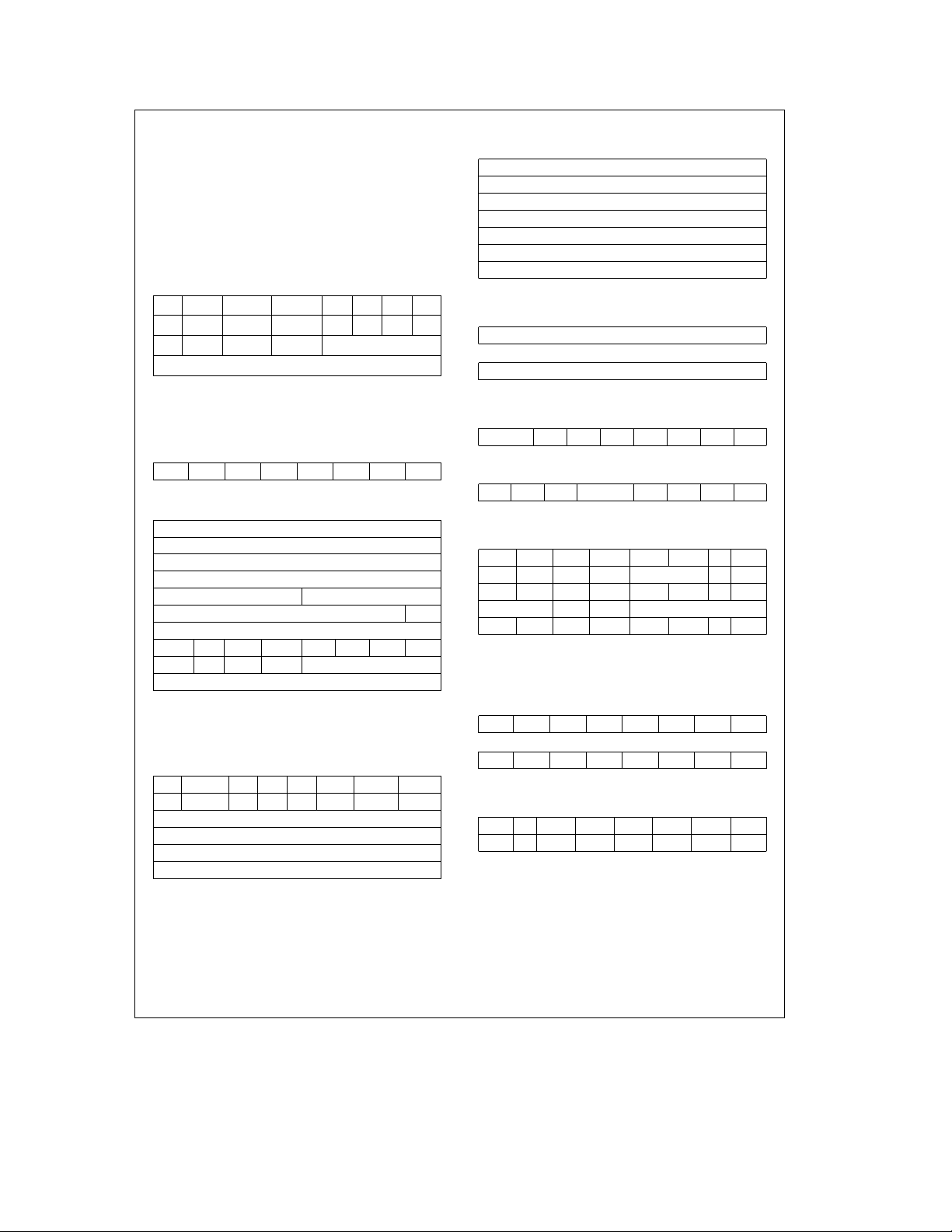
4.0 Command Set Description
The following is a table of the PC8477B command set. Each
command contains a unique first command byte called the
opcode byte which will identify to the controller how many
command bytes to expect. If an invalid command byte is
issued to the controller, it will immediately go into the Result
Phase and the status will be 80 (hex), which signifies Invalid
Command.
4.1 COMMAND SET SUMMARY
CONFIGURE
Command Phase
0 0 0 1 0011
0 0 0 0 0000
0 EIS FIFO POLL THRESH
PRETRK
Execution Phase: Internal registers written.
No Result Phase
DUMPREG
Command Phase
00001110
Execution Phase: Internal registers read.
Result Phase
PTR Drive 0
PTR Drive 1
PTR Drive 2
PTR Drive 3
Step Rate Time Motor Off Time
Motor On Time DMA
Sectors per Track/End of Track
LOCK 0 DC3 DC2 DC1 DC0 GAP WG
0 EIS FIFO POLL THRESH
PRETRK
Note: Sectors per Track parameter returned if last command issued was
Format. End of Track parameter returned if last command issued was Read
or Write.
FORMAT TRACK
Command Phase
0 MFM 0 0 1 1 0 1
X X XXXHDDR1DR0
Bytes per Sector
Sectors per Track
Format Gap
Data Pattern
Execution Phase: System transfers four ID bytes (track,
head, sector, bytes/sector) per sector to the floppy controller via DMA or Non-DMA modes. The entire track is formatted. The data block in the Data Field of each sector is filled
with the data pattern byte.
Result Phase
Status Register 0
Status Register 1
Status Register 2
Undefined
Undefined
Undefined
Undefined
INVALID
Command Phase
Invalid Op Codes
Result Phase
Status Register 0 (80 hex)
LOCK
Command Phase
LOCK 0 0 1 0 1 0 0
Execution Phase: Internal register is written.
Result Phase
0 0 0 LOCK 0 0 0 0
MODE
Command Phase
0000 0001
TMR IAF IPS 0 LOW PWR 1 ETR
FWR FRD BST R255 0 0 0 0
DENSEL BFR WLD Head Settle
0000 0RGOPU
Execution Phase: Internal registers are written.
No Result Phase
NSC
Command Phase
00011000
Result Phase
01110011
PERPENDICULAR MODE
Command Phase
00010010
OW 0 DC3 DC2 DC1 DC0 GAP WG
Execution Phase: Internal registers are written.
No Result Phase
15
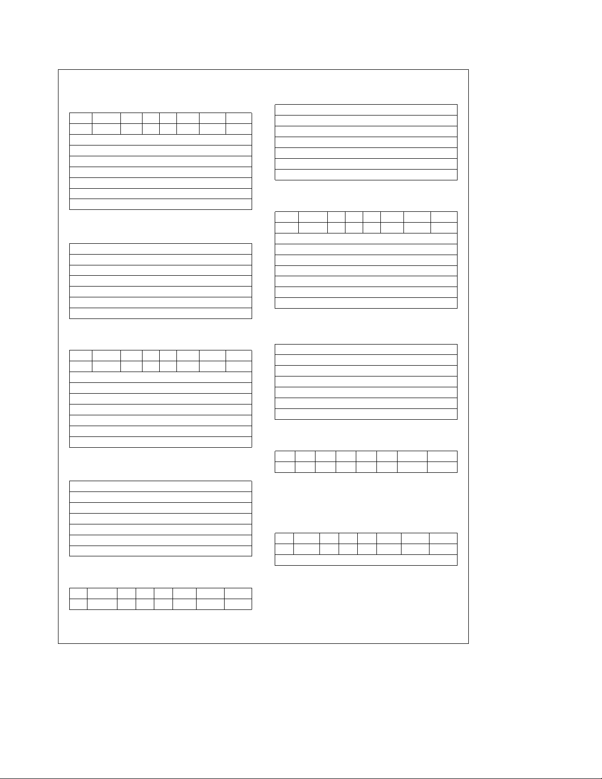
4.0 Command Set Description (Continued)
READ DATA
Command Phase
MT MFM SK 0 0 1 1 0
IPS X X X X HD DR1 DR0
Track Number
Drive Head Number
Sector Number
Bytes per Sector
End of Track Sector Number
Intersector Gap Length
Data Length
Execution Phase: Data read from disk drive is transferred
to system via DMA or Non-DMA modes.
Result Phase
Status Register 0
Status Register 1
Status Register 2
Track Number
Head Number
Sector Number
Bytes per Sector
READ DELETED DATA
Command Phase
MT MFM SK 0 1 1 0 0
IPS X X X X HD DR1 DR0
Track Number
Drive Head Number
Sector Number
Bytes per Sector
End of Track Sector Number
Intersector Gap Length
Data Length
Execution Phase: Data read from disk drive is transferred
to system via DMA or Non-DMA modes.
Result Phase
Status Register 0
Status Register 1
Status Register 2
Track Number
Head Number
Sector Number
Bytes per Sector
READ ID
Command Phase
0 MFM 0 0 1 0 1 0
X X XXXHDDR1DR0
Execution Phase: Controller reads first ID Field header
bytes it can find and reports these bytes to the system in the
result bytes.
Result Phase
Status Register 0
Status Register 1
Status Register 2
Track Number
Head Number
Sector Number
Bytes per Sector
READ A TRACK
Command Phase
0 MFM 0 0 0 0 1 0
IPS X XXXHDDR1DR0
Track Number
Drive Head Number
Sector Number
Bytes per Sector
End of Track Sector Number
Intersector Gap Length
Data Length
Execution Phase: Data read from disk drive is transferred
to system via DMA or Non-DMA modes.
Result Phase
Status Register 0
Status Register 1
Status Register 2
Track Number
Head Number
Sector Number
Bytes per Sector
RECALIBRATE
Command Phase
000001 1 1
0 0 0 0 0 0 DR1 DR0
Execution Phase: Disk drive head is stepped out to
Track 0.
No Result Phase
RELATIVE SEEK
Command Phase
1 DIR 0 0 1 1 1 1
X X X X X HD DR1 DR0
Relative Track Number
Execution Phase: Disk drive head stepped in or out a
programmable number of tracks.
No Result Phase
16
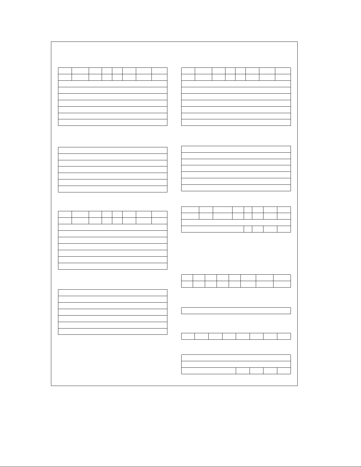
4.0 Command Set Description (Continued)
SCAN EQUAL
Command Phase
MT MFM SK 1 0 0 0 1
IPS X X X X HD DR1 DR0
Track Number
Drive Head Number
Sector Number
Bytes per Sector
End of Track Sector Number
Intersector Gap Length
Sector Step Size
Execution Phase: Data transferred from system to
controller is compared to data read from disk.
Result Phase
Status Register 0
Status Register 1
Status Register 2
Track Number
Head Number
Sector Number
Bytes per Sector
SCAN HIGH OR EQUAL
Command Phase
MT MFM SK 1 1 1 0 1
IPS X X X X HD DR1 DR0
Track Number
Drive Head Number
Sector Number
Bytes per Sector
End of Track Sector Number
Intersector Gap Length
Sector Step Size
Execution Phase: Data transferred from system to
controller is compared to data read from disk.
Result Phase
Status Register 0
Status Register 1
Status Register 2
Track Number
Head Number
Sector Number
Bytes per Sector
SCAN LOW OR EQUAL
Command Phase
MT MFM SK 1 1 0 0 1
IPS X X X X HD DR1 DR0
Track Number
Drive Head Number
Sector Number
Bytes per Sector
End of Track Sector Number
Intersector Gap Length
Sector Step Size
Execution Phase: Data transferred from system to
controller is compared to data read from disk.
Result Phase
Status Register 0
Status Register 1
Status Register 2
Track Number
Head Number
Sector Number
Bytes per Sector
SEEK
Command Phase
00 001111
X X X X X HD DR1 DR0
New Track Number
MSN of Track Number 0 0 0 0
Note: Last Command Phase byte is required only if ETR is set in Mode
Command.
Execution Phase: Disk drive head is stepped in or out to a
programmable track.
No Result Phase
SENSE DRIVE STATUS
Command Phase
00000 1 0 0
XXXXXHDDR1DR0
Execution Phase: Disk drive status information is detected
and reported.
Result Phase
Status Register 3
SENSE INTERRUPT
Command Phase
00001000
Execution Phase: Status of interrupt is reported.
Result Phase
Status Register 0
Present Track Number (PTR)
MSNofPTR 0000
Note: Third Result Phase byte can only be read if ETR is set in the Mode
Command.
17
 Loading...