NSC NSC800D-3, NSC800D-3I, NSC800E-3M, NSC800E-4I, NSC800N-1 Datasheet
...
TL/C/5171
NSC800 High-Performance Low-Power CMOS Microprocessor
June 1992
NSC800TMHigh-Performance
Low-Power CMOS Microprocessor
General Description
The NSC800 is an 8-bit CMOS microprocessor that functions as the central processing unit (CPU) in National Semiconductor’s NSC800 microcomputer family. National’s
microCMOS technology used to fabricate this device provides system designers with performance equivalent to
comparable NMOS products, but with the low power advantage of CMOS. Some of the many system functions incorporated on the device, are vectored priority interrupts, refresh
control, power-save feature and interrupt acknowledge. The
NSC800 is available in dual-in-line and surface mounted
chip carrier packages.
The system designer can choose not only from the dedicated CMOS peripherals that allow direct interfacing to the
NSC800 but from the full line of National’s CMOS products
to allow a low-power system solution. The dedicated peripherals include NSC810A RAM I/O Timer, NSC858 UART,
and NSC831 I/O.
All devices are available in commercial, industrial and military temperature ranges along with two added reliability
flows. The first is an extended burn in test and the second is
the military class C screening in accordance with Method
5004 of MIL-STD-883.
Features
Y
Fully compatible with Z80Éinstruction set:
Powerful set of 158 instructions
10 addressing modes
22 internal registers
Y
Low power: 50 mW at 5V V
CC
Y
Unique power-save feature
Y
Multiplexed bus structure
Y
Schmitt trigger input on reset
Y
On-chip bus controller and clock generator
Y
Variable power supply 2.4Vb6.0V
Y
On-chip 8-bit dynamic RAM refresh circuitry
Y
Speed: 1.0 ms instruction cycle at 4.0 MHz
NSC800-4 4.0 MHz
NSC800-35 3.5 MHz
NSC800-3 2.5 MHz
NSC800-1 1.0 MHz
Y
Capable of addressing 64k bytes of memory and 256
I/O devices
Y
Five interrupt request lines on-chip
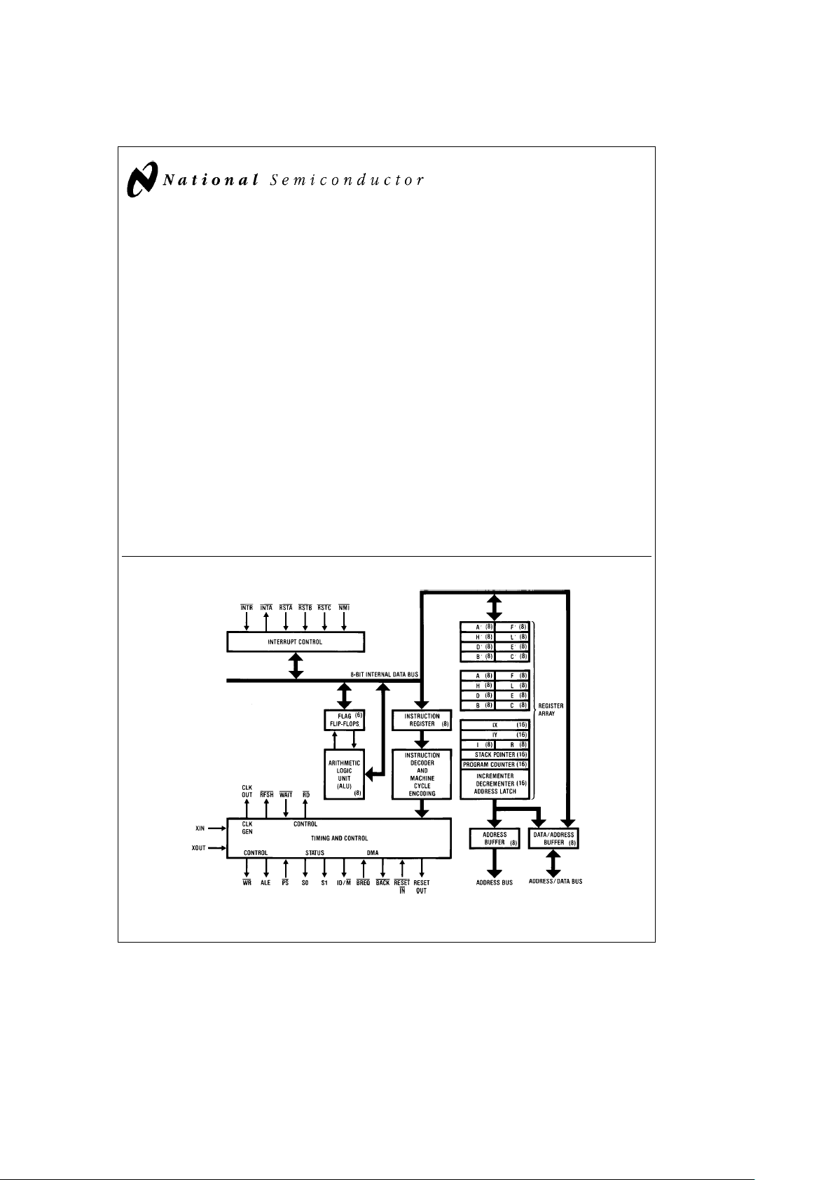
Block Diagram
TL/C/5171– 73
NSC800TMis a trademark of National Semiconductor Corp.
TRI-STATE
É
is a registered trademark of National Semiconductor Corp.
Z80
É
is a registered trademark of Zilog Corp.
C
1995 National Semiconductor Corporation RRD-B30M105/Printed in U. S. A.

Table of Contents
1.0 ABSOLUTE MAXIMUM RATINGS
2.0 OPERATING CONDITIONS
3.0 DC ELECTRICAL CHARACTERISTICS
4.0 AC ELECTRICAL CHARACTERISTICS
5.0 TIMING WAVEFORMS
NSC800 HARDWARE
6.0 PIN DESCRIPTIONS
6.1 Input Signals
6.2 Output Signals
6.3 Input/Output Signals
7.0 CONNECTION DIAGRAMS
8.0 FUNCTIONAL DESCRIPTION
8.1 Register Array
8.2 Dedicated Registers
8.2.1 Program Counter
8.2.2 Stack Pointer
8.2.3 Index Register
8.2.4 Interrupt Register
8.2.5 Refresh Register
8.3 CPU Working and Alternate Register Sets
8.3.1 CPU Working Registers
8.3.2 Alternate Registers
8.4 Register Functions
8.4.1 Accumulator
8.4.2 F RegisterÐFlags
8.4.3 Carry (C)
8.4.4 Adds/Subtract (N)
8.4.5 Parity/Overflow (P/V)
8.4.6 Half Carry (H)
8.4.7 Zero Flag (Z)
8.4.8 Sign Flag (S)
8.4.9 Additional General Purpose Registers
8.4.10 Alternate Configurations
8.5 Arithmetic Logic Unit (ALU)
8.6 Instruction Register and Decoder
9.0 TIMING AND CONTROL
9.1 Internal Clock Generator
9.2 CPU Timing
9.3 Initialization
9.4 Power Save Feature
9.0 TIMING AND CONTROL
9.5 Bus Access Control
9.6 Interrupt Control
NSC800 SOFTWARE
10.0 INTRODUCTION
11.0 ADDRESSING MODES
11.1 Register
11.2 Implied
11.3 Immediate
11.4 Immediate Extended
11.5 Direct Addressing
11.6 Register Indirect
11.7 Indexed
11.8 Relative
11.9 Modified Page Zero
11.10 Bit
12.0 INSTRUCTION SET
12.1 Instruction Set Index/Alphabetical
12.2 Instruction Set Mnemonic Notation
12.3 Assembled Object Code Notation
12.4 8-Bit Loads
12.5 16-Bit Loads
12.6 8-Bit Arithmetic
12.7 16-Bit Arithmetic
12.8 Bit Set, Reset, and Test
12.9 Rotate and Shift
12.10 Exchanges
12.11 Memory Block Moves and Searches
12.12 Input/Output
12.13 CPU Control
12.14 Program Control
12.15 Instruction Set: Alphabetical Order
12.16 Instruction Set: Numerical Order
13.0 DATA ACQUISITION SYSTEM
14.0 NSC800M/883B MIL STD 883/CLASS C
SCREENING
15.0 BURN-IN CIRCUITS
16.0 ORDERING INFORMATION
17.0 RELIABILITY INFORMATION
2

1.0 Absolute Maximum Ratings (Note 1)
If Military/Aerospace specified devices are required,
please contact the National Semiconductor Sales
Office/Distributors for availability and specifications.
Storage Temperature
b
65§Ctoa150§C
Voltage on Any Pin
with Respect to Ground
b
0.3V to V
CC
a
0.3V
Maximum V
CC
7V
Power Dissipation 1W
Lead Temp. (Soldering, 10 seconds) 300
§
C
2.0 Operating Conditions
NSC800-1
x
T
A
e
0§Ctoa70§C
T
A
eb
40§Ctoa85§C
NSC800-3
x
T
A
e
0§Ctoa70§C
T
A
eb
40§Ctoa85§C
T
A
eb
55§Ctoa125§C
NSC800-35/883C
x
T
A
eb
55§Ctoa125§C
NSC800-4
x
T
A
e
0§Ctoa70§C
T
A
eb
40§Ctoa85§C
NSC800-4MIL
x
T
A
eb
55§Ctoa90§C
3.0 DC Electrical Characteristics V
CC
e
5Vg10%, GNDe0V, unless otherwise specified.
Symbol Parameter Conditions Min Typ Max Units
V
IH
Logical 1 Input Voltage 0.8 V
CC
V
CC
V
V
IL
Logical 0 Input Voltage 0 0.2 V
CC
V
V
HY
Hysteresis at RESET IN input V
CC
e
5V 0.25 0.5 V
V
OH1
Logical 1 Output Voltage I
OUT
eb
1.0 mA 2.4 V
V
OH2
Logical 1 Output Voltage I
OUT
eb
10 mAV
CC
b
0.5 V
V
OL1
Logical 0 Output Voltage I
OUT
e
2 mA 0 0.4 V
V
OL2
Logical 0 Output Voltage I
OUT
e
10 mA 0 0.1 V
I
IL
Input Leakage Current 0sV
IN
s
V
CC
b
10.0 10.0 mA
I
OL
Output Leakage Current 0sV
IN
s
V
CC
b
10.0 10.0 mA
I
CC
Active Supply Current I
OUT
e
0, f
(XIN)
e
2 MHz, T
A
e
25§C 8 11 mA
I
CC
Active Supply Current I
OUT
e
0, f
(XIN)
e
5 MHz, T
A
e
25§C1015mA
I
CC
Active Supply Current I
OUT
e
0, f
(XIN)
e
7 MHz,
15 21 mA
T
A
e
25§C
I
CC
Active Supply Current I
OUT
e
0, f
(XIN)
e
8 MHz, T
A
e
25§C1521mA
I
Q
Quiescent Current I
OUT
e
0, PSe0, V
IN
e
0orV
IN
e
V
CC
25mA
f
(XIN)
e
0 MHz, T
A
e
25§C, X
IN
e
0, CLKe1
I
PS
Power-Save Current I
OUT
e
0, PSe0, V
IN
e
0orV
IN
e
V
CC
57mA
f
(XIN)
e
5.0 MHz , T
A
e
25
§
C
IN
Input Capacitance 610pF
C
OUT
Output Capacitance 812pF
VCCPower Supply Voltage (Note 2) 2.4 5 6 V
Note 1: Absolute Maximum Ratings indicate limits beyond which permanent damage may occur. Continuous operation at these limits is not intended and should be
limited to those conditions specified under DC Electrical Characteristics.
Note 2: CPU operation at lower voltages will reduce the maximum operating speed. Operation at voltages other than 5V
g
10% is guaranteed by design, not
tested.
3
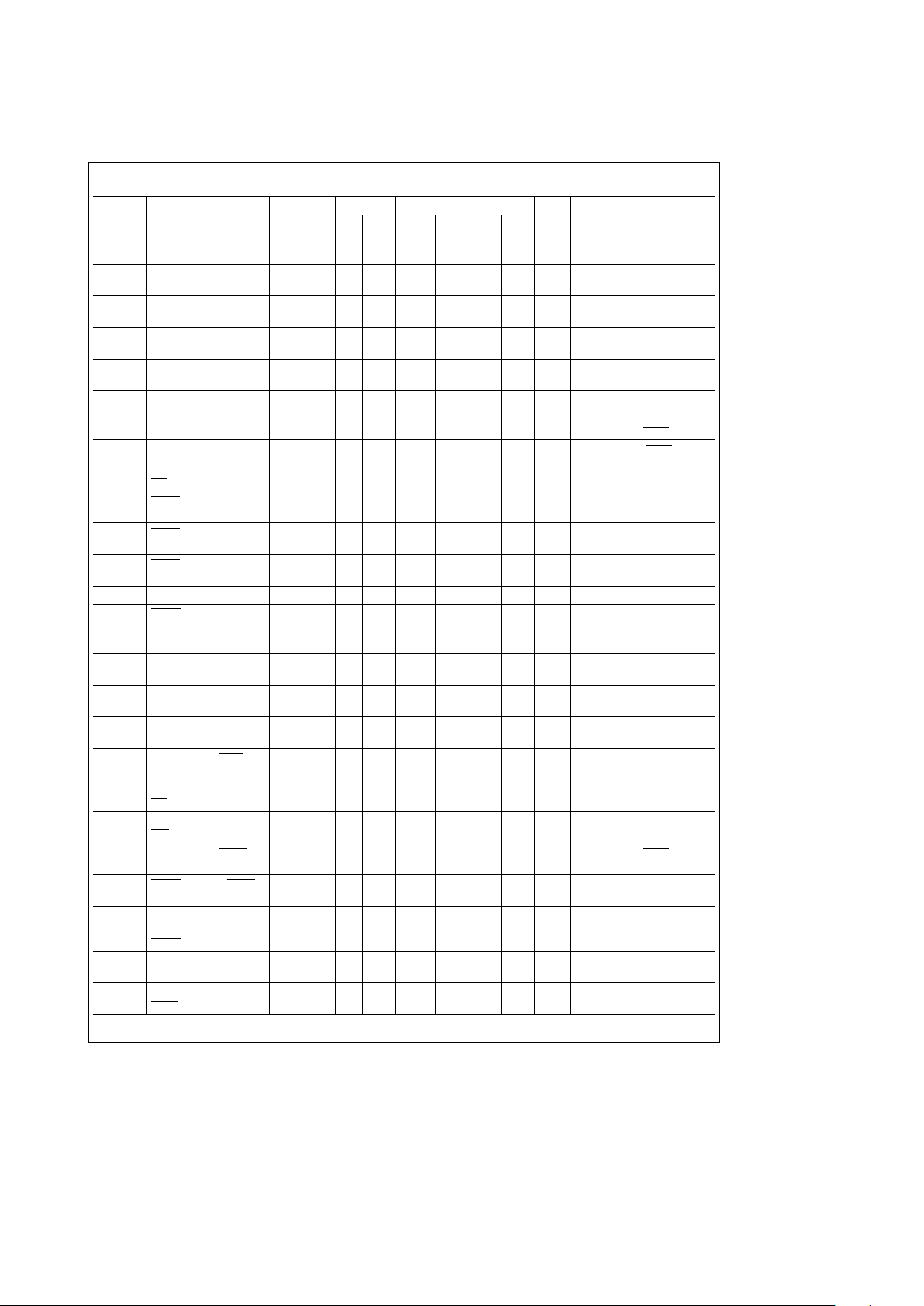
4.0 AC Electrical Characteristics V
CC
e
5Vg10%, GNDe0V, unless otherwise specified
Symbol Parameter
NSC800-1 NSC800-3 NSC800-35 NSC800-4
Units Notes
Min Max Min Max Min Max Min Max
t
X
Period at XIN and XOUT 500 3333 200 3333 142 3333 125 3333 ns
Pins
T Period at Clock Output 1000 6667 400 6667 284 6667 250 6667 ns
(
e
2tX)
t
R
Clock Rise Time 110 110 90 80 ns Measured from
10%–90% of signal
t
F
Clock Fall Time 70 60 55 50 ns Measured from
10%–90% of signal
t
L
Clock Low Time 435 150 90 80 ns 50% duty cycle, square
wave input on XIN
t
H
Clock High Time 450 145 85 75 ns 50% duty cycle, square
wave input on XIN
t
ACC(OP)
ALE to Valid Data 1340 490 340 300 ns Add t for each WAIT STATE
t
ACC(MR)
ALE to Valid Data 1875 620 405 360 ns Add t for each WAIT STATE
t
AFR
AD(0–7) Float after 0 0 0 0 ns
RD
Falling
t
BABE
BACK Rising to Bus 1000 400 300 250 ns
Enable
t
BABF
BACK Falling to 50 50 50 50 ns
Bus Float
t
BACL
BACK Fall to CLK 425 125 60 55 ns
Falling
t
BRH
BREQ Hold Time 0 0 0 0 ns
t
BRS
BREQ Set-Up Time 100 50 50 45 ns
t
CAF
Clock Falling ALE 0 70 0 65 0 60 0 55 ns
Falling
t
CAR
Clock Rising to ALE 0 100 0 100 0 90 0 80 ns
Rising
t
CRD
Clock Rising to 100 90 90 80 ns
Read Rising
t
CRF
Clock Rising to 80 70 70 65 ns
Refresh Falling
t
DAI
ALE Falling to INTA 445 160 95 85 ns
Falling
t
DAR
ALE Falling to 400 575 160 250 100 180 90 160 ns
RD
Falling
t
DAW
ALE Falling to 900 1010 350 420 225 300 200 265 ns
WR
Falling
t
D(BACK)1
ALE Falling to BACK 2460 975 635 560 ns Add t for each WAIT state
Falling Add t for opcode fetch cycles
t
D(BACK)2
BREQ Rising to BACK 500 1610 200 700 140 540 125 475 ns
Rising
t
D(I)
ALE Falling to INTR, 1360 475 284 250 ns Add t for each WAIT state
NMI
, RSTA-C,PS, Add t for opcode fetch cycles
BREQ
, Inputs Valid
t
DPA
Rising PS to 500 1685 200 760 140 580 125 510 ns See
Figure 14
also
Falling ALE
t
D(WAIT)
ALE Falling to 550 250 170 125 ns
WAIT
Input Valid
OPÐ Opcode Fetch
MRÐ Memory Read
4
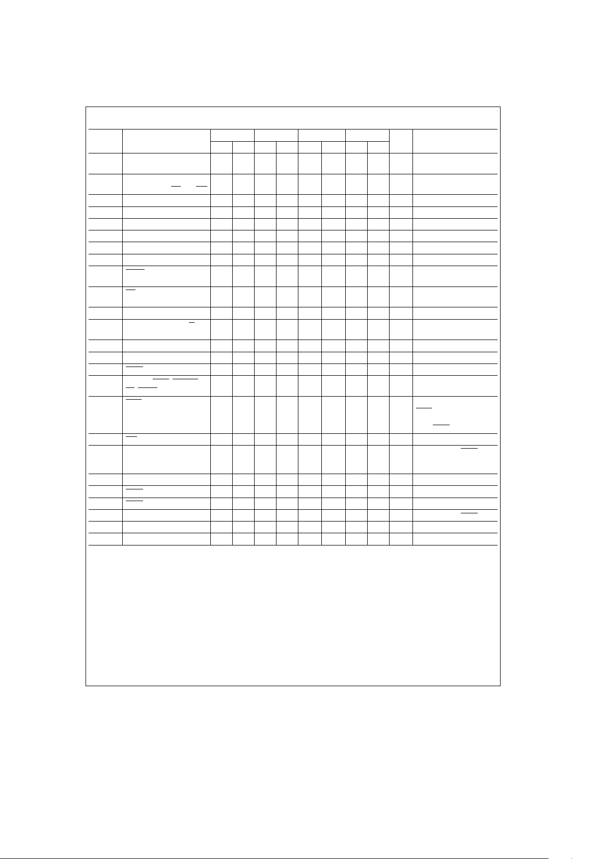
4.0 AC Electrical Characteristics V
CC
e
5Vg10%, GNDe0V, unless otherwise specified (Continued)
Symbol Parameter
NSC800-1 NSC800-3 NSC800-35 NSC800-4
Units Notes
Min Max Min Max Min Max Min Max
T
H(ADH)1
A(8–15) Hold Time During 0 0 0 0 ns
Opcode Fetch
T
H(ADH)2
A(8–15) Hold Time During 400 100 85 60 ns
Memory or IO, RD
and WR
T
H(ADL)
AD(0–7) Hold Time 100 60 35 30 ns
T
H(WD)
Write Data Hold Time 400 100 85 75 ns
t
INH
Interrupt Hold Time 0 0 0 0 ns
t
INS
Interrupt Set-Up Time 100 50 50 45 ns
t
NMI
Width of NMI Input 50 30 25 20 ns
t
RDH
Data Hold after Read 0 0 0 0 ns
t
RFLF
RFSH Rising to ALE 60 50 45 40 ns
Falling
t
RL(MR)
RD Rising to ALE Rising 390 100 50 45 ns
(Memory Read)
t
S(AD)
AD(0–7) Set-Up Time 300 45 45 40 ns
t
S(ALE)
A(8–15), SO, SI, IO/M 350 70 55 50 ns
Set-Up Time
t
S(WD)
Write Data Set-Up Time 385 75 35 30 ns
t
W(ALE)
ALE Width 430 130 115 100 ns
t
WH
WAIT Hold Time 0 0 0 0 ns
t
W(I)
Width of INTR, RSTA-C, 500 200 140 125 ns
PS
, BREQ
t
W(INTA)
INTA Strobe Width 1000 400 225 200 ns Add two t states for first
INTA of each interrupt
response string Add t for
each WAIT state
t
WL
WR Rising to ALE Rising 450 130 70 70 ns
t
W(RD)
Read Strobe Width During 960 360 210 185 ns Add t for each WAIT
State Add t/2 for Memory
Opcode Fetch
Read Cycles
t
W(RFSH)
Refresh Strobe Width 1925 725 450 395 ns
t
WS
WAIT Set-Up Time 100 70 60 55 ns
t
W(WAIT)
WAIT Input Width 550 250 195 175 ns
t
W(WR)
Write Strobe Width 985 370 250 220 ns Add t for each WAIT state
t
XCF
XIN to Clock Falling 25 100 15 95 5 90 5 80 ns
t
XCR
XIN to Clock Rising 25 85 15 85 5 90 5 80 ns
Note 1: Test conditions: te1000 ns for NSC800-1, 400 ns for NSC800, 285 ns for NSC800-35, 250 ns for NSC800-4.
Note 2: Output timings are measured with a purely capacitive load of 100 pF.
5
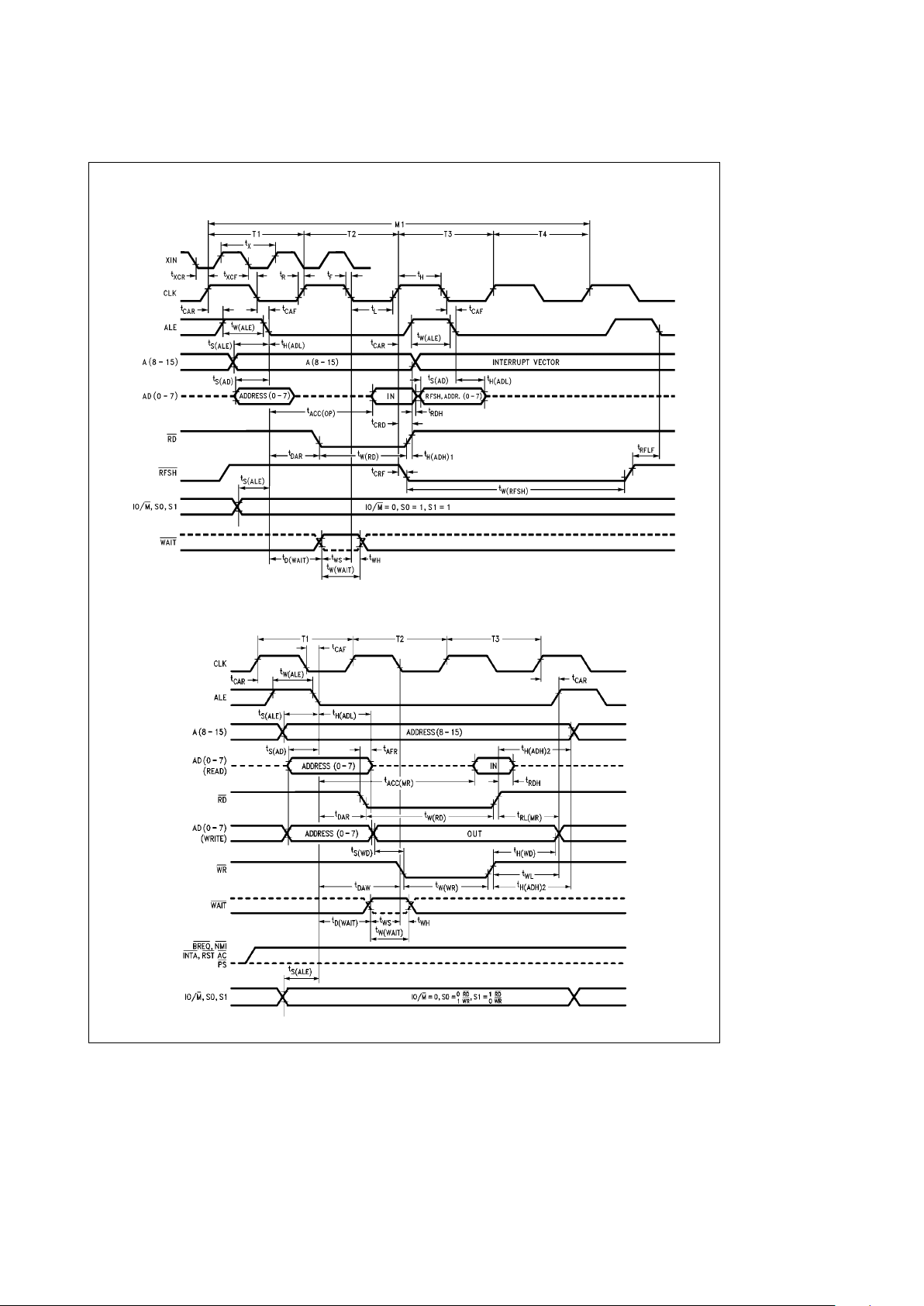
5.0 Timing Waveforms
Opcode Fetch Cycle
TL/C/5171– 3
Memory Read and Write Cycle
TL/C/5171– 4
6
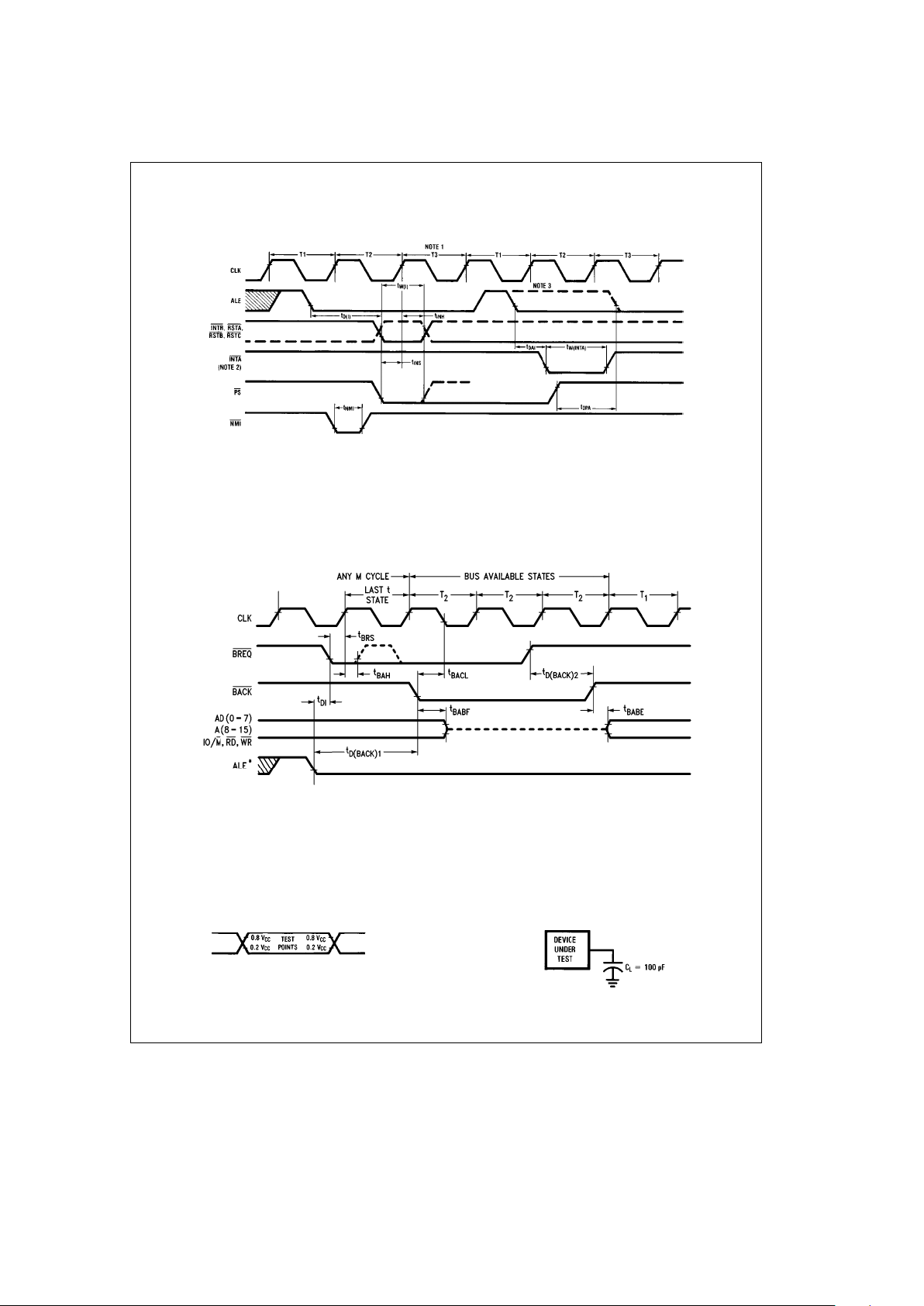
5.0 Timing Waveforms (Continued)
InterruptÐPower-Save Cycle
TL/C/5171– 5
Note 1: This t state is the last t state of the last M cycle of any instruction.
Note 2: Response to INTR input.
Note 3: Response to PS input.
Bus Acknowledge Cycle
TL/C/5171– 6
*Waveform not drawn to proportion. Use only for specifying test points.
AC Testing Input/Output Waveform
TL/C/5171– 7
AC Testing Load Circuit
TL/C/5171– 8
7

NSC800 HARDWARE
6.0 Pin Descriptions
6.1 INPUT SIGNALS
Reset Input (RESET IN): Active low. Sets A (8 –15) and AD
(0–7) to TRI-STATE
É
(high impedance). Clears the contents of PC, I and R registers, disables interrupts, and activates reset out.
Bus Request (BREQ
): Active low. Used when another de-
vice requests the system bus. The NSC800 recognizes
BREQ
at the end of the current machine cycle, and sets
A(8–15), AD(0–7), IO/M
,RD, and WR to the high imped-
ance state. RFSH
is high during a bus request cycle. The
CPU acknowledges the bus request via the BACK
output
signal.
Non-Maskable Interrupt (NMI
): Active low. The non-mask-
able interrupt, generated by the peripheral device(s), is the
highest priority interrupt. The edge sensitive interrupt requires only a pulse to set an internal flip-flop which generates the internal interrupt request. The NMI
flip-flop is monitored on the same clock edge as the other interrupts. It
must also meet the minimum set-up time spec for the interrupt to be accepted in the current machine instruction.
When the processor accepts the interrupt the flip-flop resets
automatically. Interrupt execution is independent of the interrupt enable flip-flop. NMI
execution results in saving the
PC on the stack and automatic branching to restart address
X’0066 in memory.
Restart Interrupts, A, B, C (RSTA
, RSTB, RSTC): Active
low level sensitive. The CPU recognizes restarts generated
by the peripherals at the end of the current instruction, if
their respective interrupt enable and master enable bits are
set. Execution is identical to NMI
except the interrupts vec-
tor to the following restart addresses:
Name
Restart
Address (X’)
NMI
0066
RSTA
003C
RSTB
0034
RSTC
002C
INTR
(Mode 1) 0038
The order of priority is fixed. The list above starts with the
highest priority.
Interrupt Request (INTR
): Active low, level sensitive. The
CPU recognizes an interrupt request at the end of the current instruction provided that the interrupt enable and master interrupt enable bits are set. INTR
is the lowest priority
interrupt. Program control selects one of three response
modes which determines the method of servicing INTR
in
conjunction with INTA
. See Interrupt Control.
Wait (WAIT): Active low. When set low during RD,WRor
INTA
machine cycles (during the WR machine cycle, wait
must be valid prior to write going active) the CPU extends its
machine cycle in increments of t (wait) states. The wait machine cycle continues until the WAIT
input returns high.
The wait strobe input will be accepted only during machine
cycles that have RD
,WRor INTA strobes and during the
machine cycle immediately after an interrupt has been accepted by the CPU. The later cycle has its RD strobe suppressed but it will still accept the wait.
Power-Save (PS
): Active low. PS is sampled during the last
t state of the current instruction cycle. When PS
is low, the
CPU stops executing at the end of current instruction and
keeps itself in the low-power mode. Normal operation resumes when PS
returns high (see Power Save Feature de-
scription).
CRYSTAL (X
IN,XOUT
): XINcan be used as an external
clock input. A crystal can be connected across X
IN
and
X
OUT
to provide a source for the system clock.
6.2 OUTPUT SIGNALS
Bus Acknowledge (BACK
): Active low. BACK indicates to
the bus requesting device that the CPU bus and its control
signals are in the TRI-STATE mode. The requesting device
then commands the bus and its control signals.
Address Bits 8 – 15[A(8–15)]: Active high. These are the
most significant 8 bits of the memory address during a
memory instruction. During an I/O instruction, the port address on the lower 8 address bits gets duplicated onto A(8–
15). During a BREQ/BACK cycle, the A(8 –15) bus is in the
TRI-STATE mode.
Reset Out (RESET OUT): Active high. When RESET OUT
is high, it indicates the CPU is being reset. This signal is
normally used to reset the peripheral devices.
Input/Output/Memory (IO/M
): An active high on the IO/M
output signifies that the current machine cycle is an input/
output cycle. An active low on the IO/M
output signifies that
the current machine cycle is a memory cycle. It is TRISTATE during BREQ
/BACK cycles.
Refresh (RFSH): Active low. The refresh output indicates
that the dynamic RAM refresh cycle is in progress. RFSH
goes low during T3 and T4 states of all M1 cycles. During
the refresh cycle, AD(0–7) has the refresh address and
A(8–15) indicates the interrupt vector register data. RFSH
is
high during BREQ
/BACK cycles.
Address Latch Enable (ALE): Active high. ALE is active
only during the T1 state of any M cycle and also T3 state of
the M1 cycle. The high to low transition of ALE indicates
that a valid memory, I/O or refresh address is available on
the AD(0 – 7) lines.
Read Strobe (RD
): Active low. The CPU receives data via
the AD(0 –7) lines on the trailing edge of the RD
strobe. The
RD
line is in the TRI-STATE mode during BREQ/BACK cy-
cles.
Write Strobe (WR
): Active low. The CPU sends data via the
AD(0–7) lines while the WR
strobe is low. The WR line is in
the TRI-STATE mode during BREQ
/BACK cycles.
Clock (CLK): CLK is the output provided for use as a system clock. The CLK output is a square wave at one half the
input frequency.
Interrupt Acknowledge (INTA
): Active low. This signal
strobes the interrupt response vector from the interrupting
peripheral devices onto the AD(0–7) lines. INTA
is active
during the M1 cycle immediately following the t state where
the CPU recognized the INTR
interrupt request.
Two of the three interrupt request modes use INTA.In
mode 0 one to four INTA
signals strobe a one to four byte
instruction onto the AD(0 –7) lines. In mode 2 one INTA
signal strobes the lower byte of an interrupt response vector
onto the bus. In mode 1, INTA
is inactive and the CPU re-
sponse to INTR
is the same as for an NMI or restart inter-
rupt.
8
6.0 Pin Descriptions (Continued)
Status (SO, S1): Bus status outputs provide encoded infor-
mation regarding the current M cycle as follows:
Machine Cycle
Status Control
S0 S1 IO/M RD WR
Opcode Fetch 1 1 0 0 1
Memory Read 0 1 0 0 1
Memory Write 1 0 0 1 0
I/O Read 0 1 1 0 1
I/O Write 1 0 1 1 0
Halt* 00 0 0 1
Internal Operation* 01 0 1 1
Acknowledge of Int** 11 0 1 1
*ALE is not suppressed in this cycle.
**This is the cycle that occurs immediately after the CPU accepts an inter-
rupt (RSTA
, RSTB, RSTC, INTR, NMI).
Note 1: During halt, CPU continues to do dummy opcode fetch from location
following the halt instruction with a halt status. This is so CPU can continue
to do its dynamic RAM refresh.
Note 2: No early status is provided for interrupt or hardware restarts.
6.3 INPUT/OUTPUT SIGNALS
Multiplexed Address/Data[AD(0–7)]: Active high
At RD
Time: Input data to CPU.
At WR
Time: Output data from CPU.
At Falling Edge Least significant byte of address
of ALE Time: during memory reference cycle. 8-bit
port address during I/O reference
cycle.
During BREQ
/ High impedance.
BACK
Cycle:
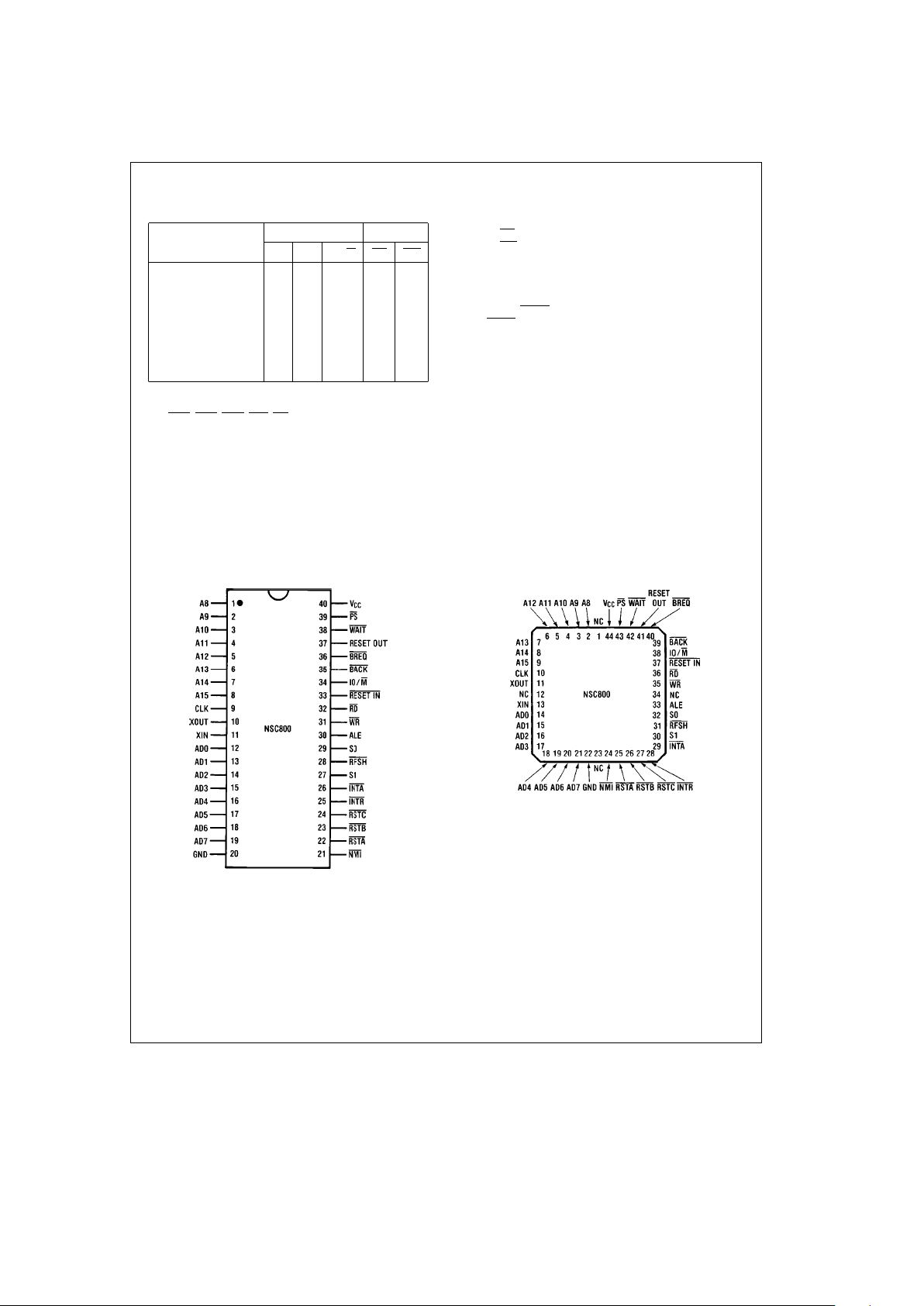
7.0 Connection Diagrams
Dual-In-Line Package
Top View
TL/C/5171– 10
Order Number NSC800D or N
See NS Package D40C or N40A
Chip Carrier Package
Top View
TL/C/5171– 11
Order Number NSC800E or V
See NS Package E44B or V44A
9
8.0 Functional Description
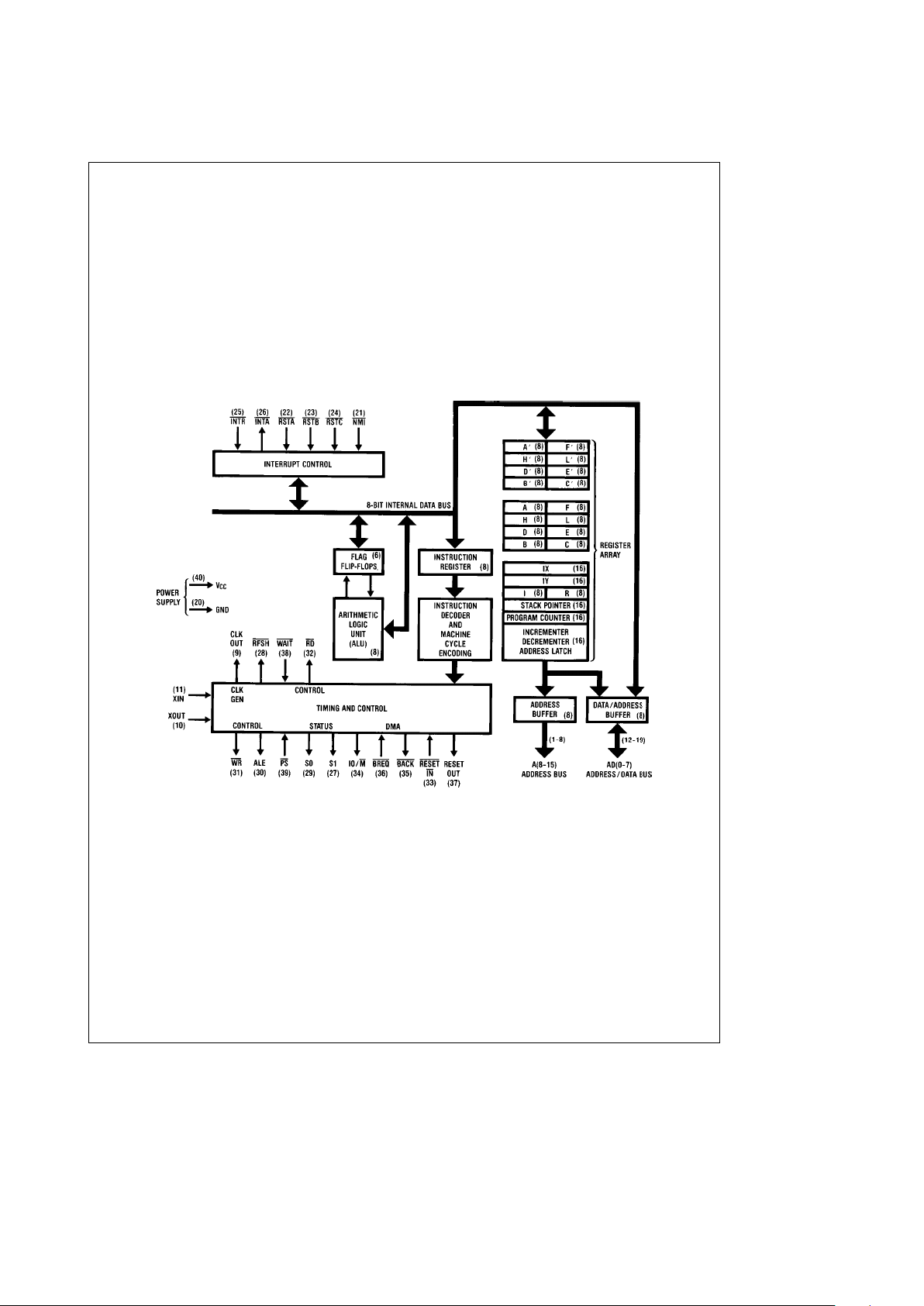
This section reviews the CPU architecture shown below, focusing on the functional aspects from a hardware perspective, including timing details.
As illustrated in
Figure 1
, the NSC800 is an 8-bit parallel
device. The major functional blocks are: the ALU, register
array, interrupt control, timing and control logic. These areas
are connected via the 8-bit internal data bus. Detailed descriptions of these blocks ae provided in the following sections.
TL/C/5171– 9
Note: Applicable pinout for 40-pin
dual-in-line package within parentheses
FIGURE 1. NSC800 CPU Functional Block Diagram
10
8.0 Functional Description (Continued)
8.1 REGISTER ARRAY
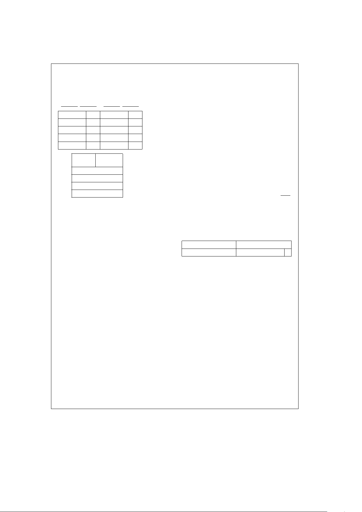
The NSC800 register array is divided into two parts: the
dedicated registers and the working registers, as shown in
Figure 2
.
Main Reg. Set Alternate Reg. Set
V â WV â W
Accumulator Flags Accumulator Flags
AFA
Ê
F
Ê
BCB
Ê
C
Ê
Working
DED
Ê
E
Ê
Registers
HLH
Ê
L
Ê
*
Interrupt Memory
Vector I Refresh R
Index Register IX Dedicated
Index Register IY
Registers
Stack Pointer SP
Program Counter PC
–
FIGURE 2. NSC800 Register Array
8.2 DEDICATED REGISTERS
There are 6 dedicated registers in the NSC800: two 8-bit
and four 16-bit registers (see
Figure 3
).
Although their contents are under program control, the program has no control over their operational functions, unlike
the CPU working registers. The function of each dedicated
register is described as follows:
CPU Dedicated Registers
Program Counter PC (16)
Stack Pointer SP (16)
Index Register IX (16)
Index Register IY (16)
Interrupt Vector Register I (8)
Memory Refresh Register R (8)
FIGURE 3. Dedicated Registers
8.2.1 Program Counter (PC)
The program counter contains the 16-bit address of the current instruction being fetched from memory. The PC increments after its contents have been transferred to the address lines. When a program jump occurs, the PC receives
the new address which overrides the incrementer.
There are many conditional and unconditional jumps, calls,
and return instructions in the NSC800’s instruction repertoire that allow easy manipulation of this register in controlling the program execution (i.e. JP NZ nn, JR Zd2, CALL
NC, nn).
8.2.2 Stack Pointer (SP)
The 16-bit stack pointer contains the address of the current
top of stack that is located in external system RAM. The
stack is organized in a last-in, first-out (LIFO) structure. The
pointer decrements before data is pushed onto the stack,
and increments after data is popped from the stack.
Various operations store or retrieve, data on the stack. This,
along with the usage of subroutine calls and interrupts, allows simple implementation of subroutine and interrupt
nesting as well as alleviating many problems of data manipulation.
8.2.3 Index Register (IX and IY)
The NSC800 contains two index registers to hold independent, 16-bit base addresses used in the indexed addressing
mode. In this mode, an index register, either IX or IY, contains a base address of an area in memory making it a pointer for data tables.
In all instructions employing indexed modes of operation,
another byte acts as a signed two’s complement displacement. This addressing mode enables easy data table manipulations.
8.2.4 Interrupt Register (I)
When the NSC800 provides a Mode 2 response to INTR
,
the action taken is an indirect call to the memory location
containing the service routine address. The pointer to the
address of the service routine is formed by two bytes, the
high-byte is from the I Register and the low-byte is from the
interrupting peripheral. The peripheral always provides an
even address for the lower byte (LSB
e
0). When the processor receives the lower byte from the peripheral it concatenates it in the following manner:
I Register External byte
8 bits 0
u
The LSB of the external byte must be zero.
FIGURE 4a. Interrupt Register
The even memory location contains the low-order byte, the
next consecutive location contains the high-order byte of
the pointer to the beginning address of the interrupt service
routine.
8.2.5 Refresh Register (R)
For systems that use dynamic memories rather than static
RAM’s, the NSC800 provides an integral 8-bit memory refresh counter. The contents of the register are incremented
after each opcode fetch and are sent out on the lower portion of the address bus, along with a refresh control signal.
This provides a totally transparent refresh cycle and does
not slow down CPU operation.
The program can read and write to the R register, although
this is usually done only for test purposes.
11

8.0 Functional Description (Continued)
8.3 CPU WORKING AND ALTERNATE REGISTER SETS
8.3.1 CPU Working Registers
The portion of the register array shown in
Figure 4b
represents the CPU working registers. These sixteen 8-bit registers are general-purpose registers because they perform a
multitude of functions, depending on the instruction being
executed. They are grouped together also due to the types
of instructions that use them, particularly alternate set operations.
The F (flag) register is a special-purpose register because
its contents are more a result of machine status rather than
program data. The F register is included because of its interaction with the A register, and its manipulations in the alternate register set operations.
8.3.2 Alternate Registers
The NSC800 registers designated as CPU working registers
have one common feature: the existence of a duplicate register in an alternate register set. This architectural concept
simplifies programming during operations such as interrupt
response, when the machine status represented by the contents of the registers must be saved.
The alternate register concept makes one set of registers
available to the programmer at any given time. Two instructions (EX AF, A‘F’ and EXX), exchange the current working
set of registers with their alternate set. One exchange between the A and F registers and their respective duplicates
(A’ and F’) saves the primary status information contained in
the accumulator and the flag register. The second exchange
instruction performs the exchange between the remaining
registers, B, C, D, E, H, and L, and their respective alternates B’, C’, D’, E’, H’, and L’. This essentially saves the
contents of the original complement of registers while providing the programmer with a usable alternate set.
CPU Main Working Register Set
Accumulator A (8) Flags F (8)
Register B (8) Register C (8)
Register D (8) Register E (8)
Register H (8) Register L (8)
CPU Alternate Working Register Set
Accumulator A’ (8) Flags F’ (8)
Register B’ (8) Register C’ (8)
Register D’ (8) Register E’ (8)
Register H’ (8) Register L’ (8)
FIGURE 4b. CPU Working and Alternate Registers
8.4 REGISTER FUNCTIONS
8.4.1 Accumulator (A Register)
The A register serves as a source or destination register for
data manipulation instructions. In addition, it serves as the
accumulator for the results of 8-bit arithmetic and logic operations.
The A register also has a special status in some types of
operations; that is, certain addressing modes are reserved
for the A register only, although the function is available for
all the other registers. For example, any register can be
loaded by immediate, register indirect, or indexed addressing modes. The A register, however, can also be loaded via
an additional register indirect addressing.
Another special feature of the A register is that it produces
more efficient memory coding than equivalent instruction
functions directed to other registers. Any register can be
rotated; however, while it requires a two-byte instruction to
normally rotate any register, a single-byte instruction is
available for rotating the contents of the accumulator (A register).
8.4.2 F Register - Flags
The NSC800 flag register consists of six status bits that
contain information regarding the results of previous CPU
operations. The register can be read by pushing the contents onto the stack and then reading it, however, it cannot
be written to. It is classified as a register because of its
affiliation with the accumulator and the existence of a duplicate register for use in exchange instructions with the accumulator.
Of the six flags shown in
Figure 5
, only four can be directly
tested by the programmer via conditional jump, call, and
return instructions. They are the Sign (S), Zero (Z), Parity/
Overflow (P/V), and Carry (C) flags. The Half Carry (H) and
Add/Subtract (N) flags are used for internal operations related to BCD arithmetic.
TL/C/5171– 23
FIGURE 5. Flag Register
12

8.0 Functional Description (Continued)
8.4.3 Carry (C)
A carry from the highest order bit of the accumulator during
an add instruction, or a borrow generated during a subtraction instruction sets the carry flag. Specific shift and rotate
instructions also affect this bit.
Two specific instructions in the NSC800 instruction repertoire set (SCF) or complement (CCF) the carry flag.
Other operations that affect the C flag are as follows:
#
Adds
#
Subtracts
#
Logic Operations (always resets C flag)
#
Rotate Accumulator
#
Rotate and Shifts
#
Decimal Adjust
#
Negation of Accumulator
Other operations do not affect the C flag.
8.4.4 Adds/Subtract (N)
This flag is used in conjunction with the H flag to ensure that
the proper BCD correction algorithm is used during the decimal adjust instruction (DAA). The correction algorithm depends on whether an add or subtract was previously done
with BCD operands.
The operations that set the N flag are:
#
Subtractions
#
Decrements (8-bit)
#
Complementing of the Accumulator
#
Block I/O
#
Block Searches
#
Negation of the Accumulator
The operations that reset the N flag are:
#
Adds
#
Increments
#
Logic Operations
#
Rotates
#
Set and Complement Carry
#
Input Register Indirect
#
Block Transfers
#
Load of the I or R Registers
#
Bit Tests
Other operations do not affect the N flag.
8.4.5 Parity/Overflow (P/V)
The Parity/Overflow flag is a dual-purpose flag that indicates results of logic and arithmetic operations. In logic operations, the P/V flag indicates the parity of the result; the
flag is set (high) if the result is even, reset (low) if the result
is odd. In arithmetic operations, it represents an overflow
condition when the result, interpreted as signed two’s complement arithmetic, is out of range for the eight-bit accumulator (i.e.
b
128 toa127).
The following operations affect the P/V flag according to
the parity of the result of the operation:
#
Logic Operations
#
Rotate and Shift
#
Rotate Digits
#
Decimal Adjust
#
Input Register Indirect
The following operations affect the P/V flag according to
the overflow result of the operation.
#
Adds (16 bit with carry, 8-bit with/without carry)
#
Subtracts (16 bit with carry, 8-bit with/without carry)
#
Increments and Decrements
#
Negation of Accumulator
The P/V flag has no significance immediately after the following operations.
#
Block I/O
#
Bit Tests
In block transfers and compares, the P/V flag indicates the
status of the BC register, always ending in the reset state
after an auto repeat of a block move. Other operations do
not affect the P/V flag.
8.4.6 Half Carry (H)
This flag indicates a BCD carry, or borrow, result from the
low-order four bits of operation. It can be used to correct the
results of a previously packed decimal add, or subtract, operation by use of the Decimal Adjust Instruction (DAA).
The following operations affect the H flag:
#
Adds (8-bit)
#
Subtracts (8-bit)
#
Increments and Decrements
#
Decimal Adjust
#
Negation of Accumulator
#
Always Set by: Logic AND
Complement Accumulator
Bit Testing
#
Always Reset By: Logic OR’s and XOR’s
Rotates and Shifts
Set Carry
Input Register Indirect
Block Transfers
Loads of I and R Registers
The H flag has no significance immediately after the following operations.
#
16-bit Adds with/without carry
#
16-Bit Subtracts with carry
#
Complement of the carry
#
Block I/O
#
Block Searches
Other operations do not affect the H flag.
13

8.0 Functional Description (Continued)
8.4.7 Zero Flag (Z)
Loading a zero in the accumulator or when a zero results
from an operation sets the zero flag.
The following operations affect the zero flag.
#
Adds (16-bit with carry, 8-bit with/without carry)
#
Subtracts (16-bit with carry, 8-bit with/without carry)
#
Logic Operations
#
Increments and Decrements
#
Rotate and Shifts
#
Rotate Digits
#
Decimal Adjust
#
Input Register Indirect
#
Block I/O (always set after auto repeat block I/O)
#
Block Searches
#
Load of I and R Registers
#
Bit Tests
#
Negation of Accumulator
The Z flag has no signficance immediately after the following operations:
#
Block Transfers
Other operations do not affect the zero flag.
8.4.8 Sign Flag (S)
The sign flag stores the state of bit 7 (the most-significant bit and sign bit) of the accumulator following an arithmetic operation. This flag is of use when dealing with signed
numbers.
The sign flag is affected by the following operation according to the result:
#
Adds (16-bit with carry, 8-bit with/without carry)
#
Subtracts (16-bit with carry, 8-bit with/without carry)
#
Logic Operations
#
Increments and Decrements
#
Rotate and Shifts
#
Rotate Digits
#
Decimal Adjust
#
Input Register Indirect
#
Block Search
#
Load of I and R Registers
#
Negation of Accumulator
The S flag has no significance immediately after the following operations:
#
Block I/O
#
Block Transfers
#
Bit Tests
Other operations do not affect the sign bit.
8.4.9 Additional General-Purpose Registers
The other general-purpose registers are the B, C, D, E, H
and L registers and their alternate register set, B’, C’, D’, E’,
H’ and L’. The general-purpose registers can be used interchangeably.
In addition, the B and C registers perform special functions
in the NSC800 expanded I/O capabilities, particularly block
I/O operations. In these functions, the C register can address I/O ports; the B register provides a counter function
when used in the register indirect address mode.
When used with the special condition jump instruction
(DJNZ) the B register again provides the counter function.
8.4.10 Alternate Configurations
The six 8-bit general purpose registers (B,C,D,E,H,L) will
combine to form three 16-bit registers. This occurs by concatenating the B and C registers to form the BC register, the
D and E registers form the DE register, and the H and L
registers form the HL register.
Having these 16-bit registers allows 16-bit data handling,
thereby expanding the number of 16-bit registers available
for memory addressing modes. The HL register typically
provides the pointer address for use in register indirect addressing of the memory.
The DE register provides a second memory pointer register
for the NSC800’s powerful block transfer operations. The
BC register also provides an assist to the block transfer
operations by acting as a byte-counter for these operations.
8.5 ARITHMETIC-LOGIC UNIT (ALU)
The arithmetic, logic and rotate instructions are performed
by the ALU. The ALU internally communicates with the registers and data buffer on the 8-bit internal data bus.
8.6 INSTRUCTION REGISTER AND DECODER
During an opcode fetch, the first byte of an instruction is
transferred from the data buffer (i.e. its on the internal data
bus) to the instruction register. The instruction register feeds
the instruction decoder, which gated by timing signals, generates the control signals that read or write data from or to
the registers, control the ALU and provide all required external control signals.
14
9.0 Timing and Control
9.1 INTERNAL CLOCK GENERATOR
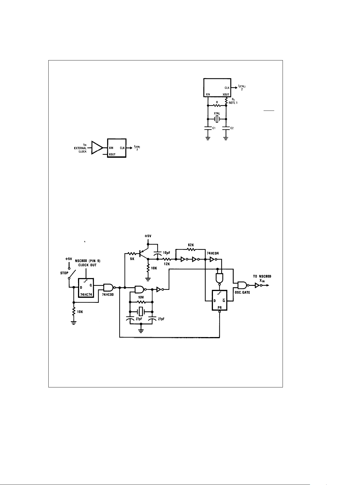
An inverter oscillator contained on the NSC800 chip provides all necessary timing signals. The chip operation frequency is equal to one half of the frequency of this oscillator.
The oscillator frequency can be controlled by one of the
following methods:
1. Leaving the X
OUT
pin unterminated and driving the X
IN
pin with an externally generated clock as shown in
Figure
6
. When driving XINwith a square wave, the minimum
duty cycle is 30% high.
TL/C/5171– 13
FIGURE 6. Use of External Clock
2. Connecting a crystal with the proper biasing network between X
IN
and X
OUT
as shown in
Figure 7
. Recommend-
ed crystal is a parallel resonance AT cut crystal.
Note 1: If the crystal frequency is between 1 MHz and 2 MHz a series
resistor, R
S
, (470X to 1500X) should be connected between
X
OUT
and R, XTAL and CZ. Additionally, the capacitance of C1
and C2 should be increased by 2 to 3 times the recommended
value. For crystal frequencies less than 1 MHz higher values of
C1 and C2 may be required. Crystal parameters will also affect
the capacitive loading requirements.
2 MHz
k
f(XTAL)
2
R
e
1MX
C1
e
20 pF
C2
e
34 pF
(Recommended)
TL/C/5171– 14
FIGURE 7. Use Of Crystal
The CPU has a minimum clock frequency input (@XIN)of
300 kHz, which results in 150 kHz system clock speed. All
registers internal to the chip are static, however there is
dynamic logic which limits the minimum clock speed. The
input clock can be stopped without fear of losing any data or
damaging the part. You stop it in the phase of the clock that
has X
IN
low and CLK OUT high. When restarting the CPU,
precautions must be taken so that the input clock meets
these minimum specification. Once started, the CPU will
continue operation from the same location at which it was
stopped. During DC operation of the CPU, typical current
drain will be 2 mA. This current drain can be reduced by
placing the CPU in a wait state during an opcode fetch cycle
then stopping the clock. For clock stop circuit, see
Figure 8
.
TL/C/5171– 36
FIGURE 8. Clock Stop Circuit
15
9.0 Timing and Control (Continued)
9.2 CPU TIMING
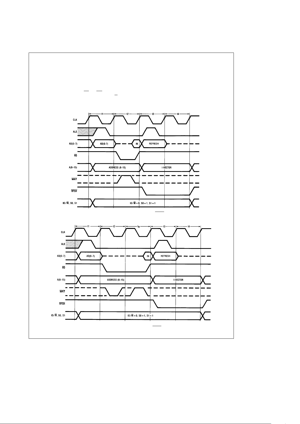
The NSC800 uses a multiplexed bus for data and addresses. The 16-bit address bus is divided into a high-order 8-bit
address bus that handles bits 8 – 15 of the address, and a
low-order 8-bit multiplexed address/data bus that handles
bits 0 – 7 of the address and bits 0 –7 of the data. Strobe
outputs from the NSC800 (ALE, RD
and WR) indicate when
a valid address or data is present on the bus. IO/M
indi-
cates whether the ensuing cycle accesses memory or I/O.
During an input or output instruction, the CPU duplicates the
lower half of the address[AD(0–7)]onto the upper address
bus[A(8–15)]. The eight bits of address will stay on A(8 –
15) for the entire machine cycle and can be used for chip
selection directly.
Figure 9
illustrates the timing relationship for opcode fetch
cycles with and without a wait state.
TL/C/5171– 15
FIGURE 9a. Opcode Fetch Cycles without WAIT
States
TL/C/5171– 16
FIGURE 9b. Opcode Fetch Cycles with WAIT States
16
9.0 Timing and Control (Continued)
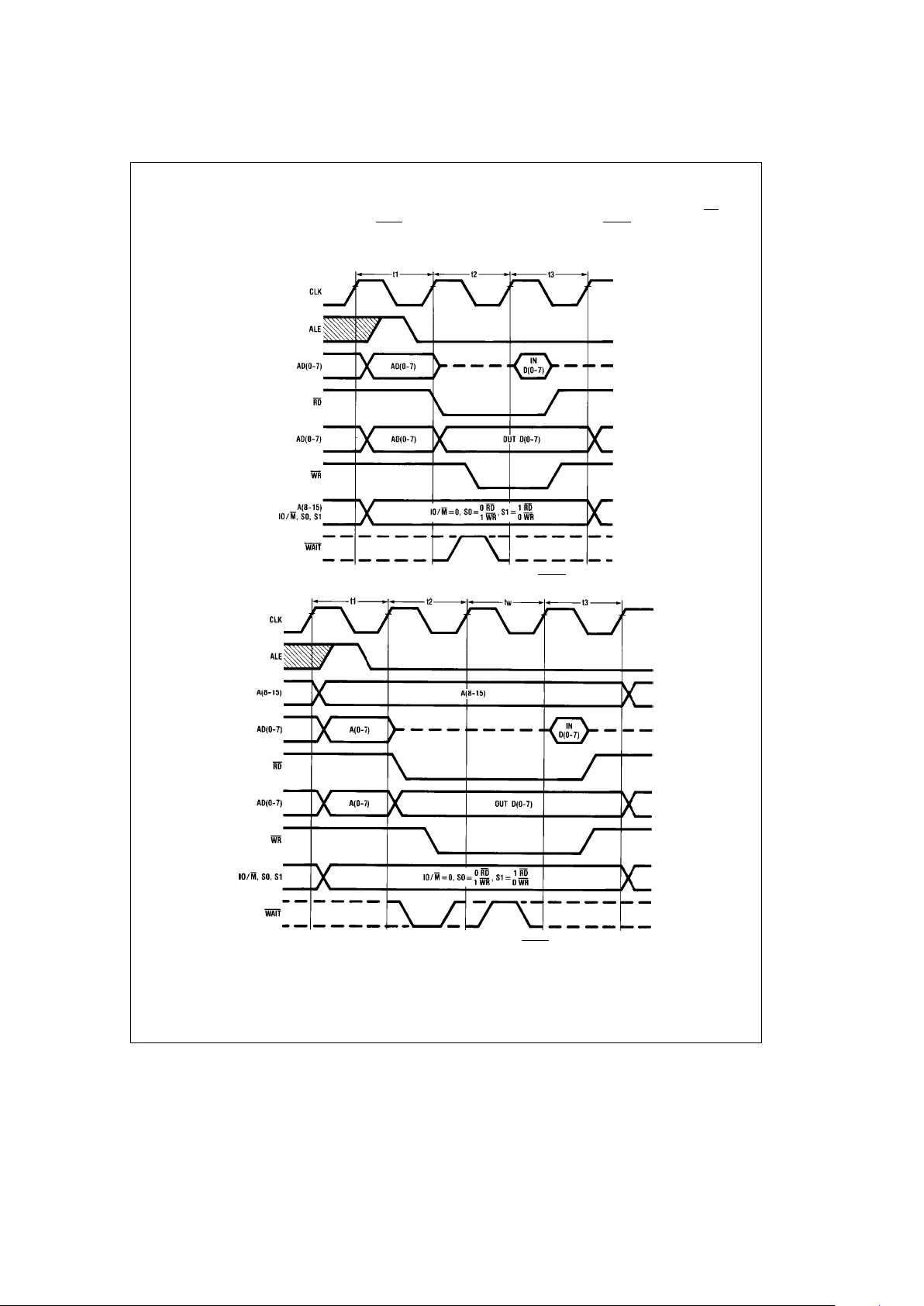
During the opcode fetch, the CPU places the contents of
the PC on the address bus. The falling edge of ALE indicates a valid address on the AD(0 –7) lines. The WAIT
input
is sampled during t
2
and if active causes the NSC800 to
insert a wait state (t
w
). WAIT is sampled again during twso
that when it goes inactive, the CPU continues its opcode
fetch by latching in the data on the rising edge of RD
from
the AD(0 – 7) lines. During t
3
, RFSH goes active and AD(0–
7) has the dynamic RAM refresh address from register R
and A(8 – 15) the interrupt vector from register I.
TL/C/5171– 17
FIGURE 10a. Memory Read/Write Cycles without WAIT States
TL/C/5171– 18
FIGURE 10b. Memory Read and Write with WAIT States
17
9.0 Timing and Control (Continued)
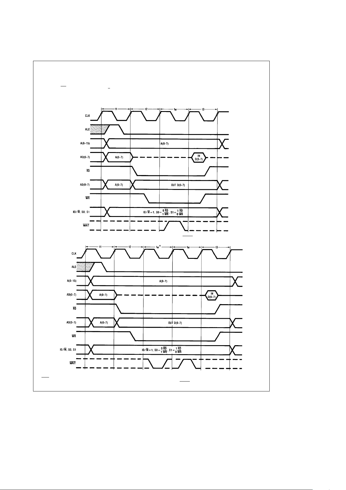
Figure 10
shows the timing for memory read (other than
opcode fetchs) and write cycles with and without a wait
state. The RD
stobe is widened by
t
2
(half the machine
state) for memory reads so that the actual latching of the
input data occurs later.
Figure 11
shows the timing for input and output cycles with
and without wait states. The CPU automatically inserts one
wait state into each I/O instruction to allow sufficient time
for an I/O port to decode the address.
TL/C/5171– 19
FIGURE 11a. Input and Output Cycles without WAIT States
TL/C/5171– 20
*WAIT state automatically inserted during IO operation.
FIGURE 11b. Input and Output Cycles with WAIT States
18
9.0 Timing and Control (Continued)
9.3 INITIALIZATION
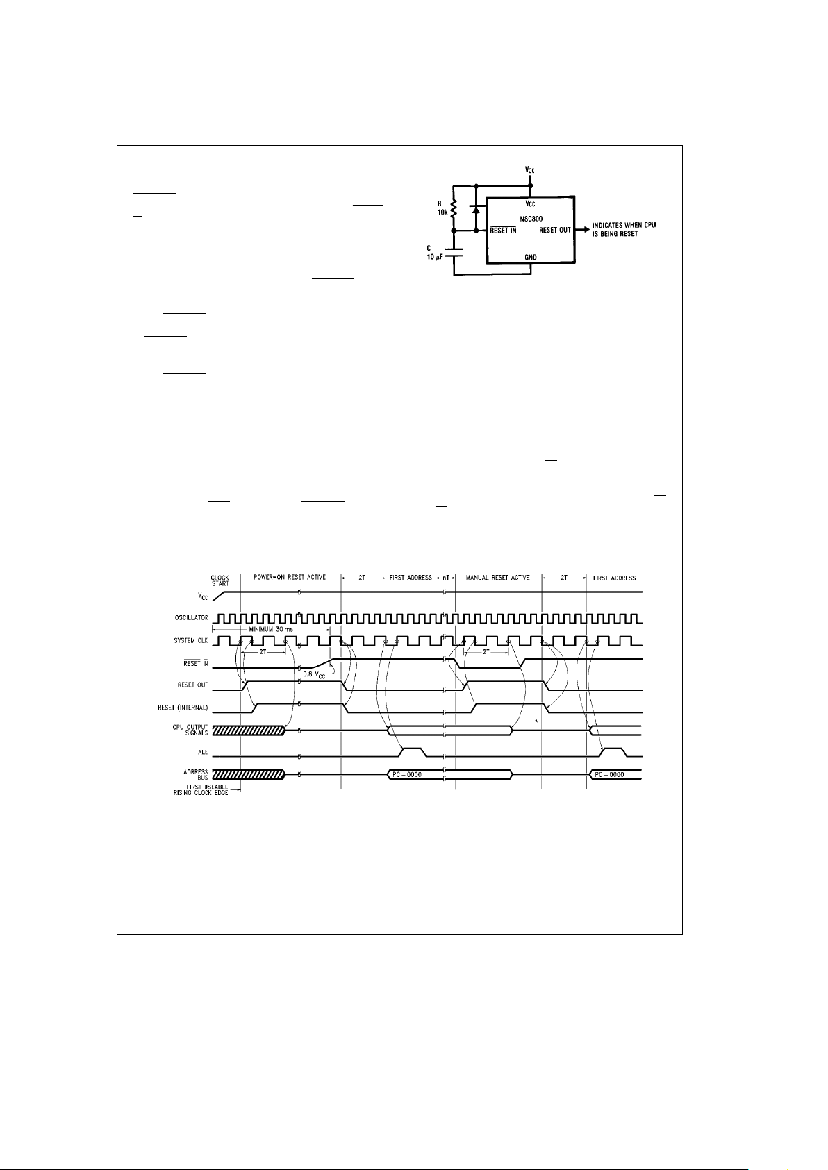
RESET IN
initializes the NSC800; RESET OUT initializes the
peripheral components. The Schmitt trigger at the RESET
IN input facilitates using an R-C network reset scheme during power up (see
Figure 12
).
To ensure proper power-up conditions for the NSC800, the
following power-up and initialization procedure is recommended:
1. Apply power (V
CC
and GND) and set RESET IN active
(low). Allow sufficient time (approximately 30 ms if a crystal is used) for the oscillator and internal clocks to stabilize. RESET IN
must remain low for at least 3t state (CLK)
times. RESET OUT goes high as soon as the active
RESET IN
signal is clocked into the first flip-flop after the
on-chip Schmitt trigger. RESET OUT signal is available to
reset the peripherals.
2. Set RESET IN
high. RESET OUT then goes low as the
inactive RESET IN
signal is clocked into the first flip-flop
after the on-chip Schmitt trigger. Following this the CPU
initiates the first opcode fetch cycle.
Note: The NSC800 initialization includes: Clear PC to
X’0000 (the first opcode fetch, therefore, is from memory
location X’0000). Clear registers I (Interrupt Vector Base)
and R (Refresh Counter) to X’00. Clear interrupt control register bits IEA, IEB and IEC. The interrupt control bit IEI is set
to 1 to maintain INS8080A/Z80A compatibility (see INTERRUPTS for more details). The CPU disables maskable interrupts and enters INTR
Mode 0. While RESET IN is active
(low), the A(8 – 15) and AD(0–7) lines go to high impedance
(TRI-STATE) and all CPU strobes go to the inactive state
(see
Figure 13
).
TL/C/5171– 21
FIGURE 12. Power-On Reset
9.4 POWER-SAVE FEATURE
The NSC800 provides a unique power-save mode by the
means of the PS
pin. PS input is sampled at the last t state
of the last M cycle of an instruction. After recognizing an
active (low) level on PS
, The NSC800 stops its internal
clocks, thereby reducing its power dissipation to one half of
operating power, yet maintaining all register values and internal control status. The NSC800 keeps its oscillator running, and makes the CLK signal available to the system.
When in power-save the ALE strobe will be stopped high
and the address lines[AD(0–7), A(8 – 15)]will indicate the
next machine address. When PS
returns high, the opcode
fetch (or M1 cycle) of the CPU begins in a normal manner.
Note this M1 cycle could also be an interrupt acknowledge
cycle if the NSC800 was interrupted simultaneously with PS
(i.e. PS has priority over a simultaneously occurring interrupt). However, interrupts are not accepted during power
save.
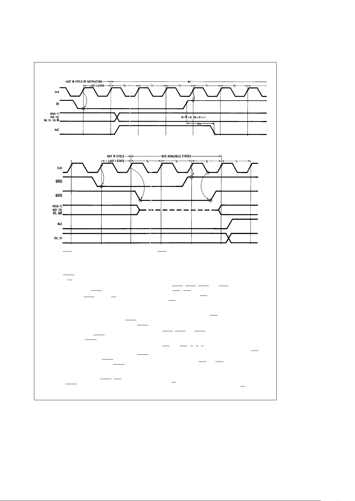
Figure 14
illustrates the power save timing.
TL/C/5171– 74
FIGURE 13. NSC800 Signals During Power-On and Manual Reset
19
9.0 Timing and Control (Continued)
TL/C/5171– 28
FIGURE 14. NSC800 Power-Save
TL/C/5171– 22
*S0, S1 during BREQ will indicate same machine cycle as during the cycle when BREQ was accepted.
t
Z
e
time states during which bus and control signals are in high impedance mode.
FIGURE 15. Bus Acknowledge Cycle
In the event BREQ
is asserted (low) at the end of an instruc-
tion cycle and PS
is active simultaneously, the following oc-
curs:
1. The NSC800 will go into BACK
cycle.
2. Upon completion of BACK cycle if PS is still active the
CPU will go into power-save mode.
9.5 BUS ACCESS CONTROL
Figure 15
illustrates bus access control in the NSC800. The
external device controller produces an active BREQ
signal
that requests the bus. When the CPU responds with BACK
then the bus and related control strobes go to high impedance (TRI-STATE) and the RFSH
signal remains high. It
should be noted that (1) BREQ
is sampled at the last t state
of any M machine cycle only. (2) The NSC800 will not acknowledge any interrupt/restart requests, and will not peform any dynamic RAM refresh functions until after BREQ
input signal is inactive high. (3) BREQ signal has priority
over all interrupt request signals, should BREQ
and interrupt
request become active simultaneously. Therefore, interrupts
latched at the end of the instruction cycle will be serviced
after a simultaneously occurring BREQ
. NMI is latched dur-
ing an active BREQ
.
9.6 INTERRUPT CONTROL
The NSC800 has five interrupt/restart inputs, four are maskable (RSTA
, RSTB, RSTC, and INTR) and one is non-mask-
able (NMI
). NMI has the highest priority of all interrupts; the
user cannot disable NMI
. After recognizing an active input
on NMI
, the CPU stops before the next instruction, pushes
the PC onto the stack, and jumps to address X’0066, where
the user’s interrupt service routine is located (i.e., restart to
memory location X’0066). NMI
is intended for interrupts requiring immediate attention, such as power-down, control
panel, etc.
RSTA
, RSTB and RSTC are restart inputs, which, if enabled,
execute a restart to memory location X’003C, X’0034, and
X’002C, respectively. Note that the CPU response to the
NMI
and RST (A,B,C) request input is basically identical,
except for the restored memory location. Unlike NMI
, how-
ever, restart request inputs must be enabled.
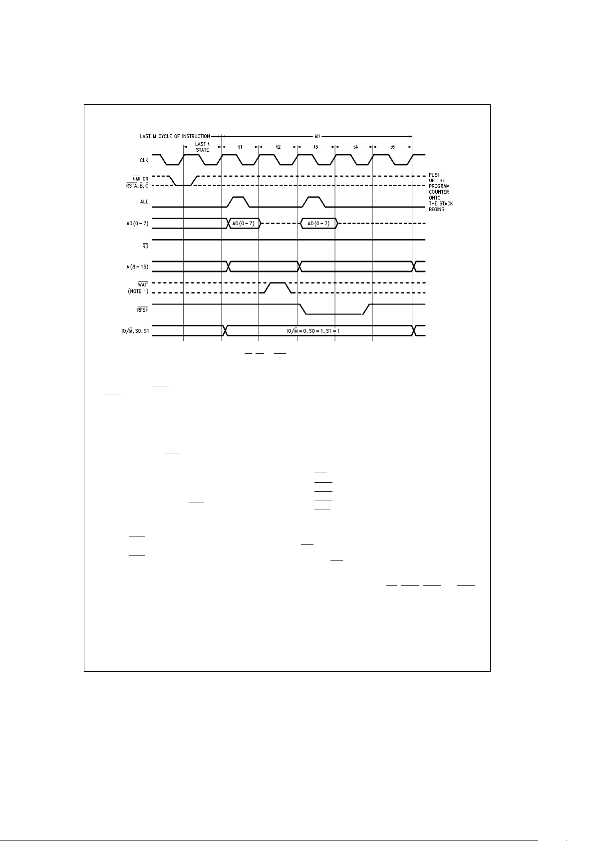
Figure 16
illustrates NMI and RST interrupt machine cycles.
M1 cycle will be a dummy opcode fetch cycle followed by
M2 and M3 which are stack push operations. The following
instruction then starts from the interrupts restart location.
Note: RD does
not
go low during this dummy opcode fetch. A unique indica-
tion of INTA can be decoded using 2 ALEs and RD
.
20
9.0 Timing and Control (Continued)
TL/C/5171– 24
Note 1: This is the only machine cycle that does not have an RD,WR, or INTA strobe but will accept a wait strobe.
FIGURE 16. Non-Maskable and Restart Interrupt Machine Cycle
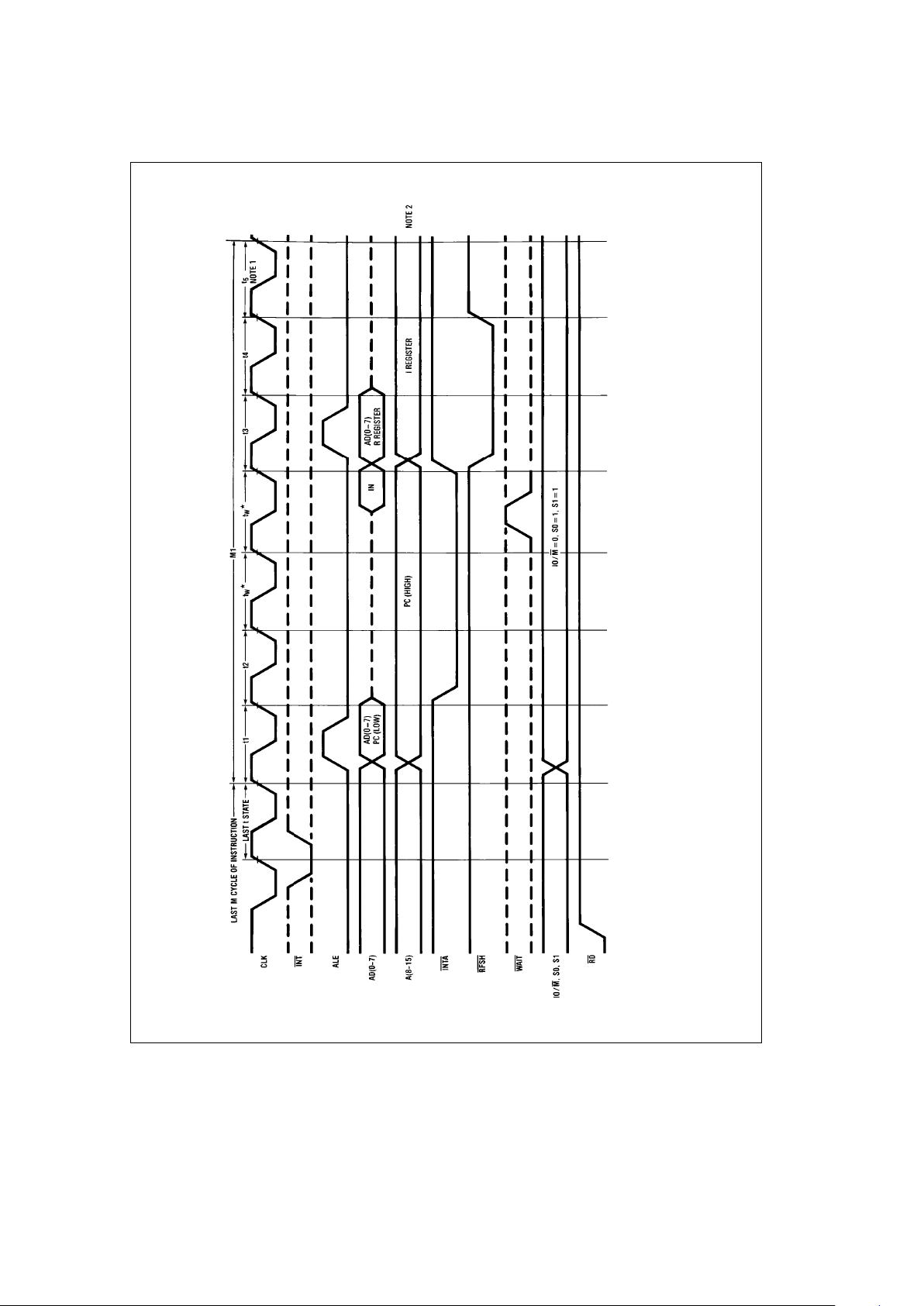
The NSC800 also provides one more general purpose interrupt request input, INTR
. When enabled, the CPU responds
to INTR
in one of the three modes defined by instruction
IM0, IM1, and IM2 for modes 0, 1, and 2, respectively. Following reset, the CPU automatically enables mode 0.
Interrupt (INTR
) Mode 0: The CPU responds to an interrupt
request by providing an INTA (interrupt acknowledge)
strobe, which can be used to gate an instruction from a
peripheral onto the data bus. The CPU inserts two wait
states during the first INTA
cycle to allow the interrupting
device (or its controller) ample time to gate the instruction
and determine external priorities (
Figure 18
). This can be
any instruction from one to four bytes. The most popular
instruction is one-byte call (restart instruction) or a threebyte call (CALL NN instruction). If it is a three-byte call, the
CPU issues a total of three INTA
strobes. The last two
(which do not include wait states) read NN.
Note: If the instruction stored in the ICU doesn’t require the PC to be
pushed onto the stack (eq. JP nn), then the PC will not be pushed.
Interrupt (INTR) Mode 1: Similar to restart interrupts except the restart location is X’0038 (
Figure 18
).
Interrupt (INTR
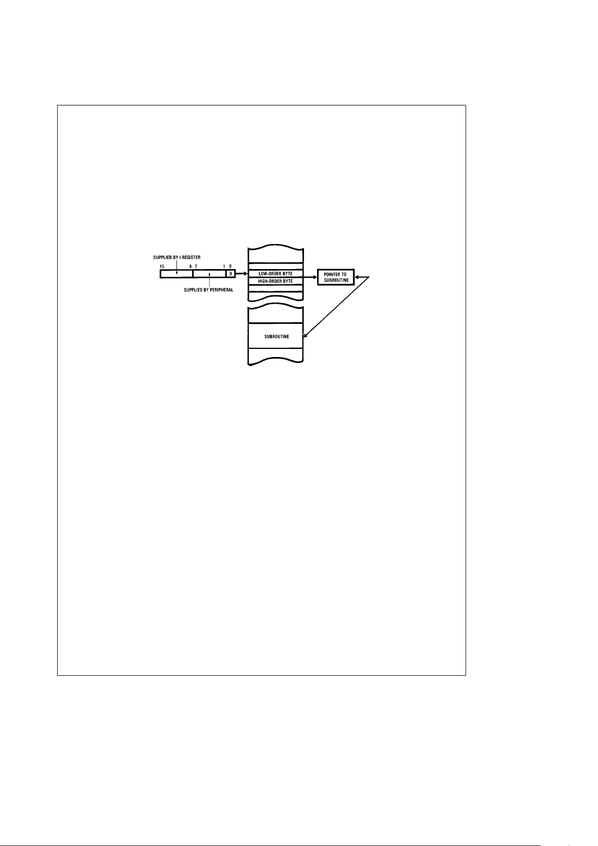
) Mode 2: With this mode, the programmer
maintains a table that contains the 16-bit starting address of
every interrupt service routine. This table can be located
anywhere in memory. When the CPU accepts a Mode 2
interrupt (
Figure 17
), it forms a 16-bit pointer to obtain the
desired interrupt service routine starting address from the
table. The upper 8 bits of this pointer are from the contents
of the I register. The lower 8 bits of the pointer are supplied
by the interrupting device with the LSB forced to zero. The
programmer must load the interrupt vector prior to the interrupt occurring. The CPU uses the pointer to get the two
adjacent bytes from the interrupt service routine starting address table to complete 16-bit service routine starting ad-
dress. The first byte of each entry in the table is the least
significant (low-order) portion of the address. The programmer must obviously fill this table with the desired addresses
before any interrupts are to be accepted.
Note that the programmer can change this table at any time
to allow peripherals to be serviced by different service routines. Once the interrupting device supplies the lower portion of the pointer, the CPU automatically pushes the program counter onto the stack, obtains the starting address
from the table and does a jump to this address.
The interrupts have fixed priorities built into the NSC800 as:
NMI
0066 (Highest Priority)
RSTA
003C
RSTB
0034
RSTC
002C
INTR
0038 (Lowest Priority)
Interrupt Enable, Interrupt Disable. The NSC800 has two
types of interrupt inputs, a non-maskable interrupt and four
software maskable interrupts. The non-maskable interrupt
(NMI
) cannot be disabled by the programmer and will be
accepted whenever a peripheral device requests an interrupt. The NMI
is usually reserved for important functions
that must be serviced when they occur, such as imminent
power failure. The programmer can selectively enable or
disable maskable interrupts (INT
, RSTA, RSTB and RSTC).
This selectivity allows the programmer to disable the maskable interrupts during periods when timing constraints don’t
allow program interruption.
There are two interrupt enable flip-flops (IFF
1
and IFF2)on
the NSC800. Two instructions control these flip-flops. Enable Interrupt (EI) and Disable Interrupt (DI). The state of
IFF
1
determines the enabling or disabling of the maskable
interrupts, while IFF
2
is used as a temporary storage loca-
tion for the state of IFF
1
.
21
9.0 Timing and Control (Continued)
A reset to the CPU will force both IFF
1
and IFF2to the reset
state disabling maskable interrupts. They can be enabled by
an EI instruction at any time by the programmer. When an EI
instruction is executed, any pending interrupt requests will
not be accepted until after the instruction following EI has
been executed. This single instruction delay is necessary in
situations where the following instruction is a return instruction and interrupts must not be allowed until the return has
been completed. The EI instruction sets both IFF
1
and IFF
2
to the enable state. When the CPU accepts an interrupt,
both IFF
1
and IFF2are automatically reset, inhibiting further
interrupts until the programmer wishes to issue a new EI
instruction. Note that for all the previous cases, IFF
1
and
IFF
2
are always equal.
The function of IFF
2
is to retain the status of IFF1when a
non-maskable interrupt occurs. When a non-maskable interrupt is accepted, IFF
1
is reset to prevent further interrupts
until reenabled by the programmer. Thus, after a non-maskable interrupt has been accepted, maskable interrupts are
disabled but the previous state of IFF
1
is saved by IFF
2
TL/C/5171– 27
FIGURE 17. Interrupt Mode 2
22
9.0 Timing and Control (Continued)
TL/C/5171– 25
*t
W
is the CPU generated WAIT state in response to an interrupt request.
Note 1: t5 will only occur in mode 1 and mode 2. During t5 the stack pointer is decremented.
Note 2: A jump to the appropriate address occurs here in mode 1 and mode 2. The CPU continues gathering data from the interrupting peripheral in mode 0 for a total of 2 –4
machine cycles. In mode 0 cycles M2 –M4 have only 1 wait state.
FIGURE 18. Interrupt Acknowledge Machine Cycle
23
 Loading...