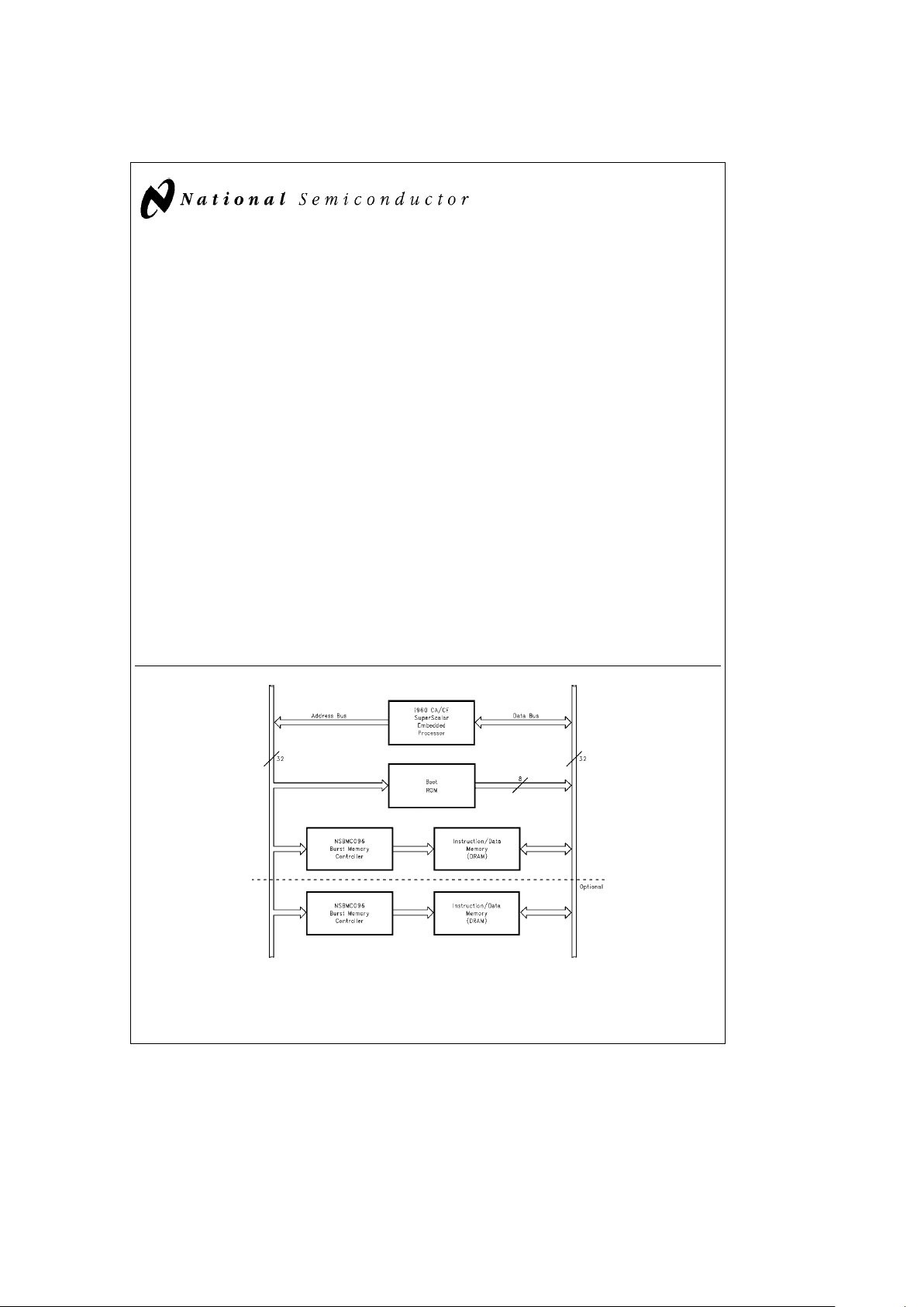
TL/V/11805
NSBMC096-16/-25/-33 Burst Memory Controller
August 1993
NSBMC096-16/-25/-33 Burst Memory Controller
General Description
The NSBMC096 Burst Memory Controller is an integrated
circuit which implements all aspects of DRAM control for
high performance systems using an i960
É
CA/CF
SuperScalar Embedded Processor. The NSBMC096 is functionally equivalent to the V96BMC
TM
.
The extremely high instruction rate achieved by these processors place extraordinary demands on memory system design if maximum throughput is to be sustained and costs
minimized.
Static RAM offers a simple solution for high speed memory
systems. However, high cost and low density make this an
expensive and space consumptive choice.
Dynamic RAMs are an attractive alternative with higher density and low cost. Their drawbacks are, slower access time
and more complex control circuitry required to operate
them.
The access time problem is solved if DRAMs are used in
page mode. In this mode, access times rival that of static
RAM. The control circuit problem is resolved by the
NSBMC096.
The function that the NSBMC096 performs is to optimally
translate the burst access protocol of the i960 CA/CF to the
page mode access protocol supported by dynamic RAMs.
The device manages one or two-way interleaved arrangements of DRAMs such that during burst access, data can be
read, or written, at the rate of one word per system clock
cycle.
The NSBMC096 has been designed to allow maximum flexibility in its application. The full range of processor speeds is
supported for a wide range of DRAM speeds, sizes and organizations.
No glue logic is required because the bus interface is customized to the i960 CA/CF. System integration is further
enhanced by providing a 24-bit heartbeat timer and a bus
watch timer on-chip.
The NSBMC096 is packaged as a 132-pin PQFP with a footprint of only 1.3 square inches. It reduces design complexity, space requirements and is fully derated for loading, temperature and voltage.
Features
Y
Interfaces directly to the i960 CA
Y
Integrated Page Cache Management
Y
Manages Page Mode Dynamic Memory devices
Y
On-chip Memory Address Multiplexer/Drivers
Y
Supports DRAMs trom 256 kB to 64 MB
Y
Bit counter/timer
Y
Non-interleaved or two way interleaved operation
Y
5-Bit Bus Watch Timer
Y
Software-configured operational parameters
Y
High-Speed/Low Power CMOS technology
Block Diagram
TL/V/11805– 1
This document contains information concerning a product that has been developed by National Semiconductor Corporation/V3 Corporation. This information
is intended to help in evaluating this product. National Semiconductor Corporation/V3 Corporation reserves the right to change and improve the specifications
of this product without notice.
TRI-STATEÉis a registered trademark of National Semiconductor Corporation.
NSBMC096
TM
and WATCHDOGTMare trademarks of National Semiconductor Corporation.
i960
É
is a registered trademark of Intel Corporation.
V96BMC
TM
is a trademark of V3 Corporation.
C
1995 National Semiconductor Corporation RRD-B30M115/Printed in U. S. A.

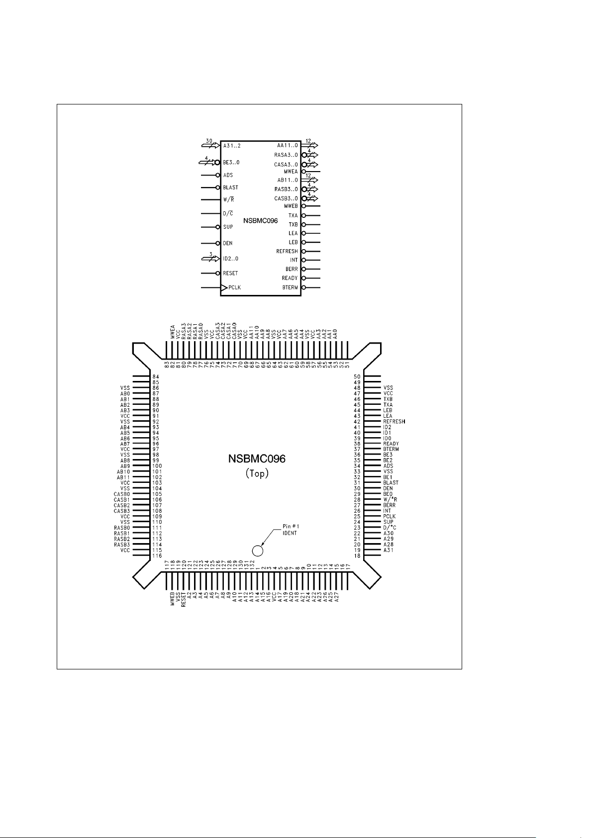
Logic and Connection Diagrams
TL/V/11805– 2
TL/V/11805– 3
Order Number NSBMC096VF
See Package Number VF132A
2

Pin Descriptions
TABLE I
Pin
Ý
Signal Name
1 A14
2 A15
3 A16
4V
CC
5 A17
6 A19
7 A20
8 A18
9 A21
10 A24
11 A22
12 A23
13 A26
14 A25
15 A27
19 A31
20 A28
21 A29
22 A30
23 D/C
24 SUP
25 PCLK
26 INT
27 BERR
28 W/R
29 BE0
30 DEN
31 BLAST
32 BE1
33 V
SS
34 ADS
35 BE2
36 BE3
37 BTERM
38 READY
39 ID0
40 ID1
41 ID2
42 REFRESH
43 LEA
Pin
Ý
Signal Name
44 LEB
45 TXA
46 TXB
47 V
CC
48 V
SS
53 AA0
54 AA1
55 AA2
56 AA3
57 V
CC
58 V
SS
59 AA4
60 AA5
61 AA6
62 AA7
63 V
CC
64 V
SS
65 AA8
66 AA9
67 AA10
68 AA11
69 V
CC
70 V
SS
71 CASA0
72 CASA1
73 CASA2
74 CASA3
75 V
CC
76 V
SS
77 RASA0
78 RASA1
79 RASA2
80 RASA3
81 V
CC
82 MWEA
86 V
SS
87 AB0
88 AB1
89 AB2
90 AB3
Pin
Ý
Signal Name
91 V
CC
92 V
SS
93 AB4
94 AB5
95 AB6
96 AB7
97 V
CC
98 V
SS
99 AB8
100 AB9
101 AB10
102 AB11
103 V
CC
104 V
SS
105 CASB0
106 CASB1
107 CASB2
108 CASB3
109 V
CC
110 V
SS
111 RASB0
112 RASB1
113 RASB2
114 RASB3
115 V
CC
118 MWEB
119 V
SS
120 RESET
121 A2
122 A3
123 A4
124 A5
125 A6
126 A7
127 A8
128 A9
129 A10
130 A11
131 A12
132 A13
Note: In order for the switching characteristics of this device to be guaranteed, it is necessary to connect all of the power pins (VCC,VSS) to the appropriate power
levels. The use of low impedance wiring to the power pins is required. In systems using the i960 CA with its attendant high switching rates, multi-layer printed circuit
boards with buried power and ground planes are required.
3

Pin Descriptions (Continued)
i960 CA/CF INTERFACE
The following pins are functionally equivalent to those on
the i960 CA/CF from which their names are taken. Like
named pins on the i960 CA/CF and the NSBMC960 are to
be wired together. All 3-State outputs are to be weakly
pulled up to V
CC
. In typical situations, a 10 kX resistor is
sufficient.
Pin Description
A2–31 Address Bus (Input): This system bus is a word address which determines the location at which an access is
required.
ADS Address Strobe (Input; Active Low): Indicates that a new access cycle is being started.
D/*C Data/*Code (Input): Signals whether an access is for data or instructions.
BLAST Burst Last (Input; Active Low): Indicates that the last cycle of a burst is in progress.
DEN Data Enable (Input; Active Low): This input is monitored by the Bus Watch Timer to detect a bus access not
returning READY.
BTERM Burst Terminate (Output; 3-State; Active Low): This output is used to request termination of a burst in progress.
Used to disable burst writes.
READY Data Ready (Output; 3-State; Active Low): The READY output is used to signal that data on the processor bus is
valid for Read, or that data has been accepted for Write.
RESET Reset (Input; Active Low): Assertion of this input sets the NSBMC960 to its initial state. Following initialization, the
NSBMC960 must be configured before any memory access is possible.
BE0–3 Byte Enable (Input; Active Low): These inputs are used to determine which byte(s) within the addressed word are to
be accessed.
W/*R WRITE/*READ (Input): This input indicates the direction which data is to be transferred to/from on the data bus.
SUP Supervisor (Input; Active Low): Indicates that the processor is operating in supervisor mode. Required for access to
configuration registers.
PCLK System Clock (Input): Processor output clock required to operate and synchronize NSBMC960 internal functions.
BERR Bus Error (Output; Active Low): When enabled, this signal is generated by the Bus Watch Circuit to prevent
processor lock-up on access to a region that is not responding.
INT Interrupt (Output; 12 mA; Active Low): This signal is assented when the 24-bit counter reaches terminal count and
interrupt out is enabled. May be programmed for pulse or handshake operation.
ID0–2 Chip ID (Input): These inputs select the address offset of the NSBMC960 configuration registers. Each NSBMC960 in
a system must have a unique address for proper operation.
4

Pin Descriptions (Continued)
MEMORY INTERFACE
The NSBMC960 is designed to drive a memory array organized as 2 leaves each of 32 bits. The address and control
signals for the memory array are output through high current
drivers in order to minimize propagation delay due to input
impedance and trace capacitance. External array drivers
are not required. The address and control signals, however,
should be externally terminated.
Pin Description
A(A,B)0–11 Multiplexed Address Bus (Output; 24 mA): These two buses transfer the multiplexed row and column
addresses to the memory array leaves A and B. When non-interleaved operation is selected, only address bus A
should be used.
RAS(A,B)0–3 Row Address Strobes (Output; 12 mA Active Low): These strobes indicate the presence of a valid row
address on busses A(A,B)0–11. These signals are to be connected one to each leaf of memory. Four banks of
interleaved memory may be attached to a NSBMC960.
CAS(A,B)0–3 Column Address Strobe (Output; 12 mA, Active Low): These strobes latch a column address from A(A,B)0 –
11. They are assigned one to each byte in a leaf.
MWE(A,B) Memory Write Enable (Output; 24 mA, Active Low): These are the DRAM write strobes. One is supplied for
each leaf to minimize signal loading.
REFRESH Refresh in progress (Output; 12 mA, Active Low): This output gives notice that a refresh cycle is to be
executed. The timing leads refresh RAS by one cycle.
BUFFER CONTROLS
Buffer control signals are provided to simplify the control of
the interface between the DRAM and i960 data busses.
Multiple operating modes facilitate choice of buffer type,
and simple bus buffers (‘‘245’’s), bus latches (‘‘543’’s) and
bus registers (‘‘646’’s) are all supported.
Pin Description
TX(A,B) Data Bus Transmit A and B (Output; Active Low): These outputs are multi-function signals. The signal names,
as they appear on the logic symbol, are the default signal names (Mode
e
0). The purpose of these outputs is to
control buffer output enables during data read transactions and, in effect, control the multiplexing of data from
each memory leaf onto the i960 CA/CF data bus.
LE(A,B) Data Bus Latch Enable A and B (Output; Active Low): These outputs are mode independent, however, the
timing of the signals change for different operational modes. They control transparent latches that hold data
transmiffed during a write transaction. In modes 0 and 1, the latch controls follow the timing of CAS for each
leaf, while in modes 2 and 3 the timing of LEA and LEB is shortened to (/2 clock.
5

Functional Description
PRODUCT OVERVIEW
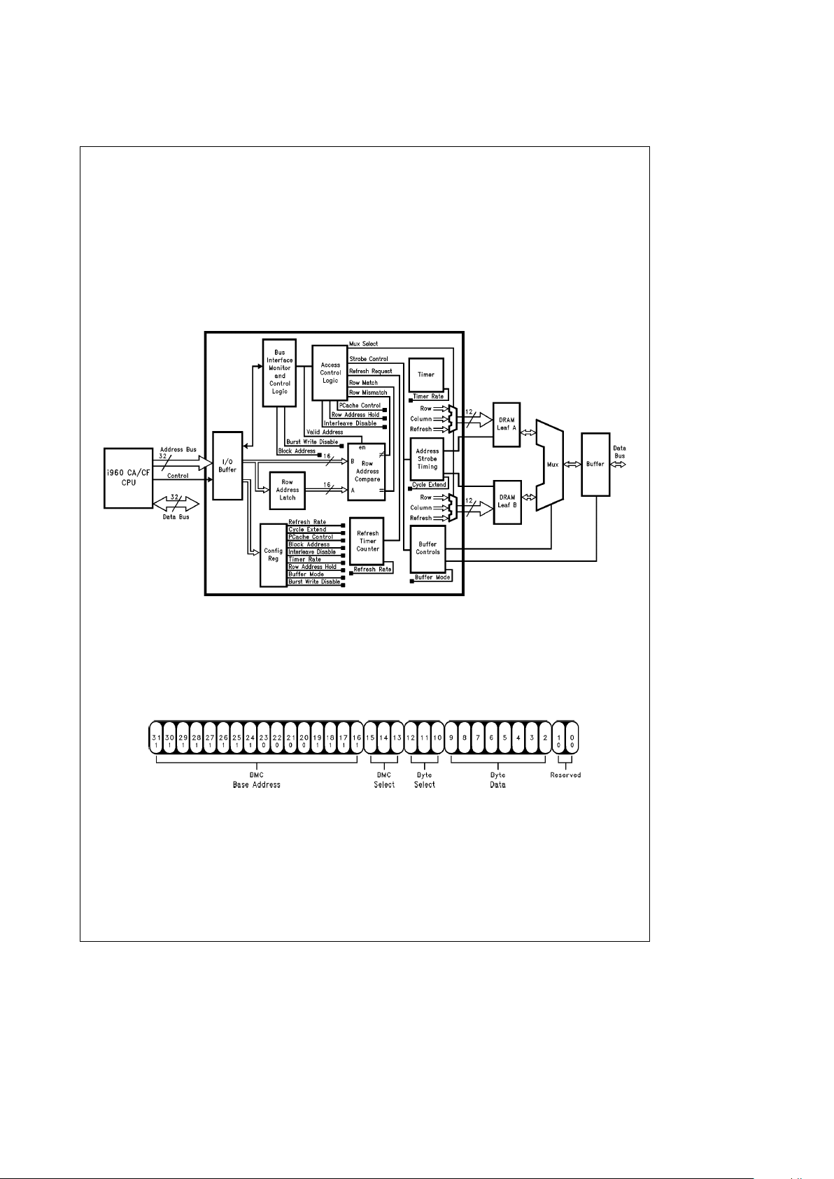
The NSBMC960 couples the i960 CA/CF interface to
DRAM access protocols, generates bus buffer and data
multiplexor controls and incorporates system and bus monitor timing resources. These functional elements are shown
in
Figure 1
. A maximum of 8 controllers may be included in a
system, each managing up to 4 banks of memory.
The NSBMC960 directly drives an array of fast page mode
DRAMs. This array may be organized as 1 or 2 leaves of
32 bits each. Standard memory sizes from 256 kbit to
64 Mbit are supported and 8-, 16-, and 32-bit access are
allowed. If interleaved mode is selected, burst access is
zero-wait-state; if memory is non-interleaved, 1-wait-state
burst access results.
The NSBMC960 allows for flexibility in the control of data
buffers to the memory array. Propagation delay is minimized
by providing these controls directly, and design flexibility
maximized by allowing the control strategy to be programmable. Buffers as diverse as 74FCT245, 74FCT543,
74FCT646, 74FCT853 and 74FCT861 may be used without
additional glue logic.
TL/V/11805– 4
FIGURE 1. Functional Block Diagram
CONFIGURATION AND CONTROL
The NSBMC960 contains 64 bits of configuration data that
controls it’s operational mode. The configuration is programmed by sending data on the address bus.
Figure 2
shows the format of a configuration access. The byte select
field determines which byte of the 64-bit field will be updat-
ed by the contents of the byte data field. Bits[1,0]are reserved and must be ‘‘0’’. The base address is fixed at
0xff0f0000 while the BMC select field must match the value
programmed at the ID[2..0]pins. In order to protect against
accidental programming, the configuration registers can
only be modified when the processor is in supervisor mode.
TL/V/11805– 5
FIGURE 2. Address Bus Fields Used to Access Configuration Data
6
 Loading...