

NSC LMV321M5X, LMV321M5, LMV321MDC, LMV321M7, LMV321M7X Datasheet
LMV321 Single/ LMV358 Dual/ LMV324 Quad
General Purpose, Low Voltage, Rail-to-Rail Output
Operational Amplifiers
General Description
The LMV358/324 are low voltage (2.7–5.5V) versions of the
dual and quad commodity op amps, LM358/324, which currently operate at 5–30V. The LMV321 is the single version.
The LMV321/358/324 are the most cost effective solutions
for the applications where low voltage operation, space saving and low price are needed. They offer specifications that
meet or exceed the familiar LM358/324. The
LMV321/358/324 haverail-to-railoutput swing capability and
the input common-mode voltage range includes ground.
They all exhibit excellent speed-power ratio, achieving
1 MHz of bandwidth and 1 V/µs of slew rate with low supply
current.
The LMV321 is available in space saving SC70-5, which is
approximately half the size of SOT23-5. The small package
saves space on pc boards, and enables the design of small
portable electronic devices. It also allows the designer to
place the device closer to the signal source to reduce noise
pickup and increase signal integrity.
The chips are built with National’s advanced submicron
silicon-gate BiCMOS process. The LMV321/358/324 have
bipolar input and output stages for improved noise performance and higher output current drive.
Features
(For V
+
=
5V and V
−
=
0V,Typical Unless Otherwise Noted)
n Guaranteed 2.7V and 5V Performance
n No Crossover Distortion
n Space Saving Package SC70-5 2.0x2.1x1.0mm
n Industrial Temp.Range −40˚C to +85˚C
n Gain-Bandwidth Product 1MHz
n Low Supply Current
LMV321 130µA
LMV358 210µA
LMV324 410µA
n Rail-to-Rail Output Swing
@
10kΩ Load V+−10mV
V
−
+65mV
n V
CM
−0.2V to V+−0.8V
Applications
n Active Filters
n General Purpose Low Voltage Applications
n General Purpose Portable Devices
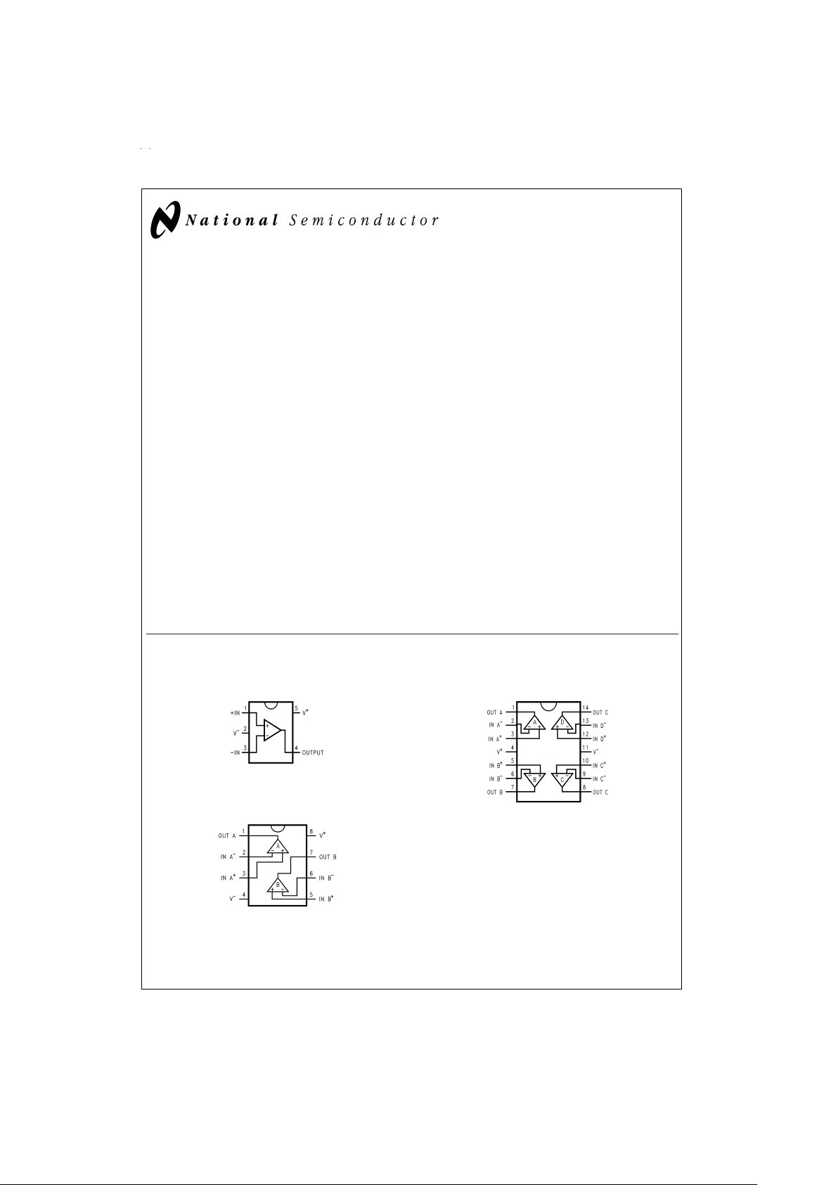
Connection Diagrams
5-Pin SC70-5/SOT23-5
DS100060-1
Top View
8-Pin SO/MSOP
DS100060-2
Top View
14-Pin SO/TSSOP
DS100060-3
Top View
August 1999
LMV321 Single/ LMV358 Dual/ LMV324 Quad General Purpose, Low Voltage, Rail-to-Rail Output
Operational Amplifiers
© 1999 National Semiconductor Corporation DS100060 www.national.com
Ordering Information
Package
Temperature Range
Packaging Marking Transport Media NSC DrawingIndustrial
−40˚C to +85˚C
5-Pin SC70-5 LMV321M7 A12 1k Units Tape and Reel MAA05
LMV321M7X A12 3k Units Tape and Reel
5-Pin SOT23-5 LMV321M5 A13 1k Units Tape and Reel MA05B
LMV321M5X A13 3k Units Tape and Reel
8-Pin Small Outline LMV358M LMV358M Rails
M08A
LMV358MX LMV358M 2.5k Units Tape and Reel
8-Pin MSOP LMV358MM LMV358 1k Units Tape and Reel
MUA08A
LMV358MMX LMV358 3.5k Units Tape and Reel
14-Pin Small Outline LMV324M LMV324M Rails
M14A
LMV324MX LMV324M 2.5k Units Tape and Reel
14-Pin TSSOP LMV324MT LMV324MT Rails
MTC14
LMV324MTX LMV324MT 2.5k Units Tape and Reel
www.national.com 2
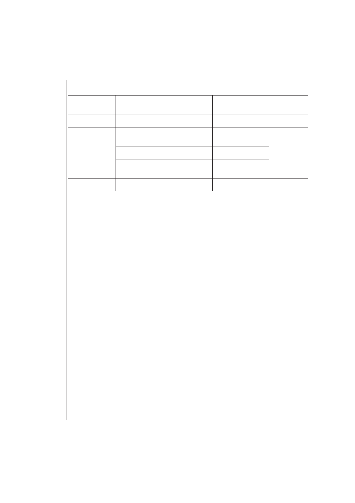
Absolute Maximum Ratings (Note 1)
If Military/Aerospace specified devices are required,
please contact the National Semiconductor Sales Office/
Distributors for availability and specifications.
ESD Tolerance (Note 2)
Machine Model 100V
Human Body Model
LMV358/324 2000V
LMV321 900V
Differential Input Voltage
±
Supply Voltage
Supply Voltage (V
+–V−
) 5.5V
Output Short Circuit to V
+
(Note 3)
Output Short Circuit to V
−
(Note 4)
Soldering Information
Infrared or Convection (20 sec) 235˚C
Storage Temp. Range −65˚C to 150˚C
Junction Temp. (T
j
, max) (Note 5) 150˚C
Operating Ratings (Note 1)
Supply Voltage 2.7V to 5.5V
Temperature Range
LMV321, LMV358, LMV324 −40˚C≤T
J
≤85˚C
Thermal Resistance (θ
JA
)(Note 10)
5-pin SC70-5 478˚C/W
5-pin SOT23-5 265˚C/W
8-Pin SOIC 190˚C/W
8-Pin MSOP 235˚C/W
14-Pin SOIC 145˚C/W
14-Pin TSSOP 155˚C/W
2.7V DC Electrical Characteristics
Unless otherwise specified, all limits guaranteed for TJ= 25˚C, V+= 2.7V, V−= 0V, VCM= 1.0V, VO=V+/2 and R
L
>
1MΩ.
Symbol Parameter Conditions Typ
(Note 6)
Limit
(Note 7)
Units
V
OS
Input Offset Voltage 1.7 7 mV
max
TCV
OS
Input Offset Voltage Average
Drift
5 µV/˚C
I
B
Input Bias Current 11 250 nA
max
I
OS
Input Offset Current 5 50 nA
max
CMRR Common Mode Rejection Ratio 0V ≤ V
CM
≤ 1.7V 63 50 dB
min
PSRR Power Supply Rejection Ratio 2.7V ≤ V
+
≤ 5V
V
O
=1V
60 50 dB
min
V
CM
Input Common-Mode Voltage
Range
For CMRR≥50dB −0.2 0 V
min
1.9 1.7 V
max
V
O
Output Swing RL= 10kΩ to 1.35V V+-10 V+-100 mV
min
60 180 mV
max
I
S
Supply Current LMV321 80 170 µA
max
LMV358
Both amplifiers
140 340 µA
max
LMV324
All four amplifiers
260 680 µA
max
www.national.com3
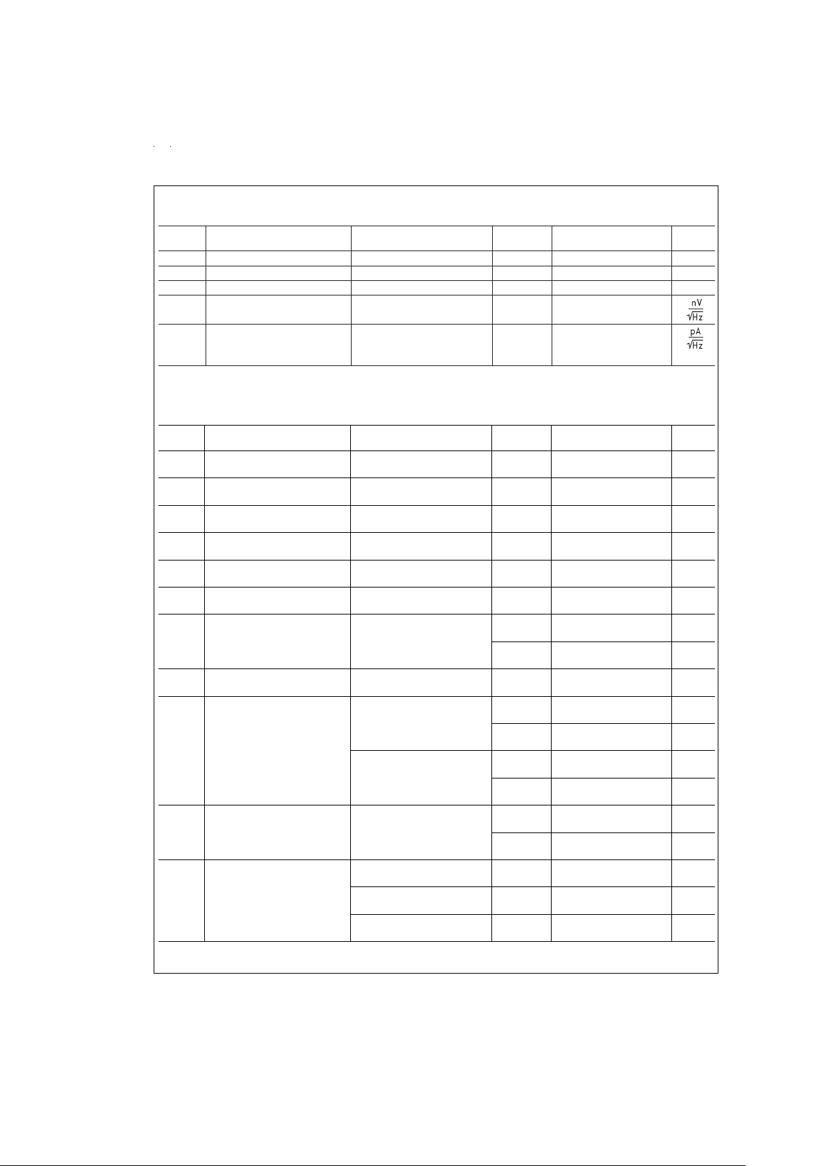
2.7V AC Electrical Characteristics
Unless otherwise specified, all limits guaranteed for TJ= 25˚C, V+= 2.7V, V−= 0V, VCM= 1.0V, VO=V+/2 and R
L
>
1MΩ.
Symbol Parameter Conditions
Typ
(Note 6)
Limit
(Note 7)
Units
GBWP Gain-Bandwidth Product C
L
= 200 pF 1 MHz
Φ
m
Phase Margin 60 Deg
G
m
Gain Margin 10 dB
e
n
Input-Referred Voltage Noise f = 1 kHz 46
i
n
Input-Referred Current Noise f = 1 kHz 0.17
5V DC Electrical Characteristics
Unless otherwise specified, all limits guaranteed for TJ= 25˚C, V+= 5V, V−= 0V, VCM= 2.0V, VO=V+/2 and R
L
>
1MΩ.
Boldface limits apply at the temperature extremes.
Symbol Parameter Conditions Typ
(Note 6)
Limit
(Note 7)
Units
V
OS
Input Offset Voltage 1.7 7
9
mV
max
TCV
OS
Input Offset Voltage Average
Drift
5 µV/˚C
I
B
Input Bias Current 15 250
500
nA
max
I
OS
Input Offset Current 5 50
150
nA
max
CMRR Common Mode Rejection Ratio 0V ≤ V
CM
≤ 4V 65 50 dB
min
PSRR Power Supply Rejection Ratio 2.7V ≤ V
+
≤ 5V
V
O
=1VVCM=1V
60 50 dB
min
V
CM
Input Common-Mode Voltage
Range
For CMRR≥50dB −0.2 0 V
min
4.2 4 V
max
A
V
Large Signal Voltage Gain
(Note 8)
RL=2kΩ 100 15
10
V/mV
min
V
O
Output Swing RL=2kΩto 2.5V V+-40 V+-300
V
+
-400
mV
min
120 300
400
mV
max
R
L
= 10kΩ to 2.5V V+-10 V+-100
V
+
-200
mV
min
65 180
280
mV
max
I
O
Output Short Circuit Current Sourcing, VO=0V 60 5 mA
min
Sinking, V
O
= 5V 160 10 mA
min
I
S
Supply Current LMV321 130 250
350
µA
max
LMV358
Both amplifiers
210 440
615
µA
max
LMV324
All four amplifiers
410 830
1160
µA
max
www.national.com 4
5V AC Electrical Characteristics
Unless otherwise specified, all limits guaranteed for TJ= 25˚C, V+= 5V, V−= 0V, VCM= 2.0V, VO=V+/2 and R
L
>
1MΩ.
Boldface limits apply at the temperature extremes.
Symbol Parameter Conditions
Typ
(Note 6)
Limit
(Note 7)
Units
SR Slew Rate (Note 9) 1 V/µs
GBWP Gain-Bandwidth Product C
L
= 200 pF 1 MHz
Φ
m
Phase Margin 60 Deg
G
m
Gain Margin 10 dB
e
n
Input-Referred Voltage Noise f = 1 kHz, 39
i
n
Input-Referred Current Noise f = 1 kHz 0.21
Note 1: Absolute Maximum Ratings indicate limits beyond which damage to the device may occur. Operating Ratings indicate conditions for which the device is intended to be functional, but specific performance is not guaranteed. For guaranteed specifications and the test conditions, see the Electrical Characteristics.
Note 2: Human body model, 1.5 kΩ in series with 100 pF. Machine model, 0Ω in series with 200 pF.
Note 3: Shorting output to V
+
will adversely affect reliability.
Note 4: Shorting output to V
-
will adversely affect reliability.
Note 5: The maximum power dissipation is a function of T
J(max)
, θJA, and TA. The maximum allowable power dissipation at any ambient temperature is PD=
(T
J(max)–TA
)/θJA. All numbers apply for packages soldered directly into a PC board.
Note 6: Typical values represent the most likely parametric norm.
Note 7: All limits are guaranteed by testing or statistical analysis.
Note 8: R
L
is connected to V-. The output voltage is 0.5V ≤ VO≤ 4.5V.
Note 9: Connected as voltage follower with 3V step input. Number specified is the slower of the positive and negative slew rates.
Note 10: All numbers are typical, and apply for packages soldered directly onto a PC board in still air.
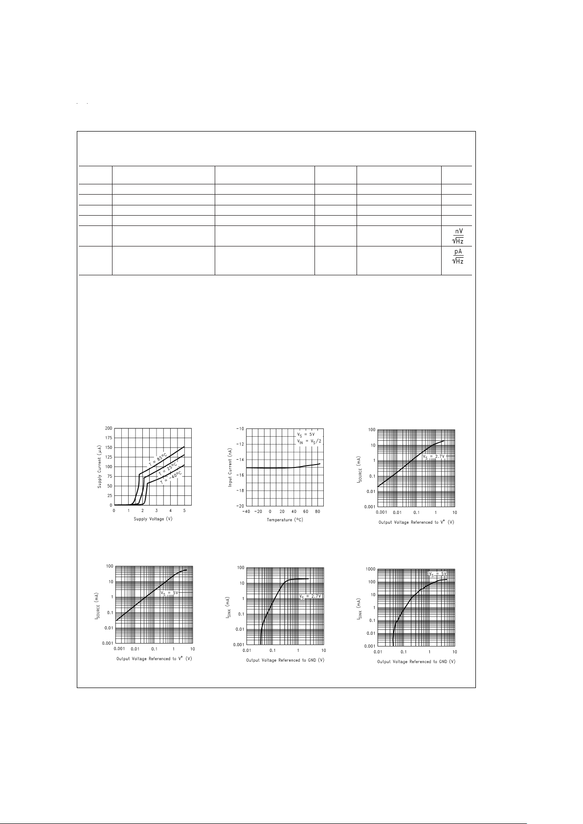
Typical Performance Characteristics Unless otherwise specified, V
S
= +5V, single supply, TA= 25˚C.
Supply Current vs Supply
Voltage (LMV321)
DS100060-73
Input Current vs
Temperature
DS100060-A9
Sourcing Current vs
Output Voltage
DS100060-69
Sourcing Current vs
Output Voltage
DS100060-68
Sinking Current vs
Output Voltage
DS100060-70
Sinking Current vs
Output Voltage
DS100060-71
www.national.com5
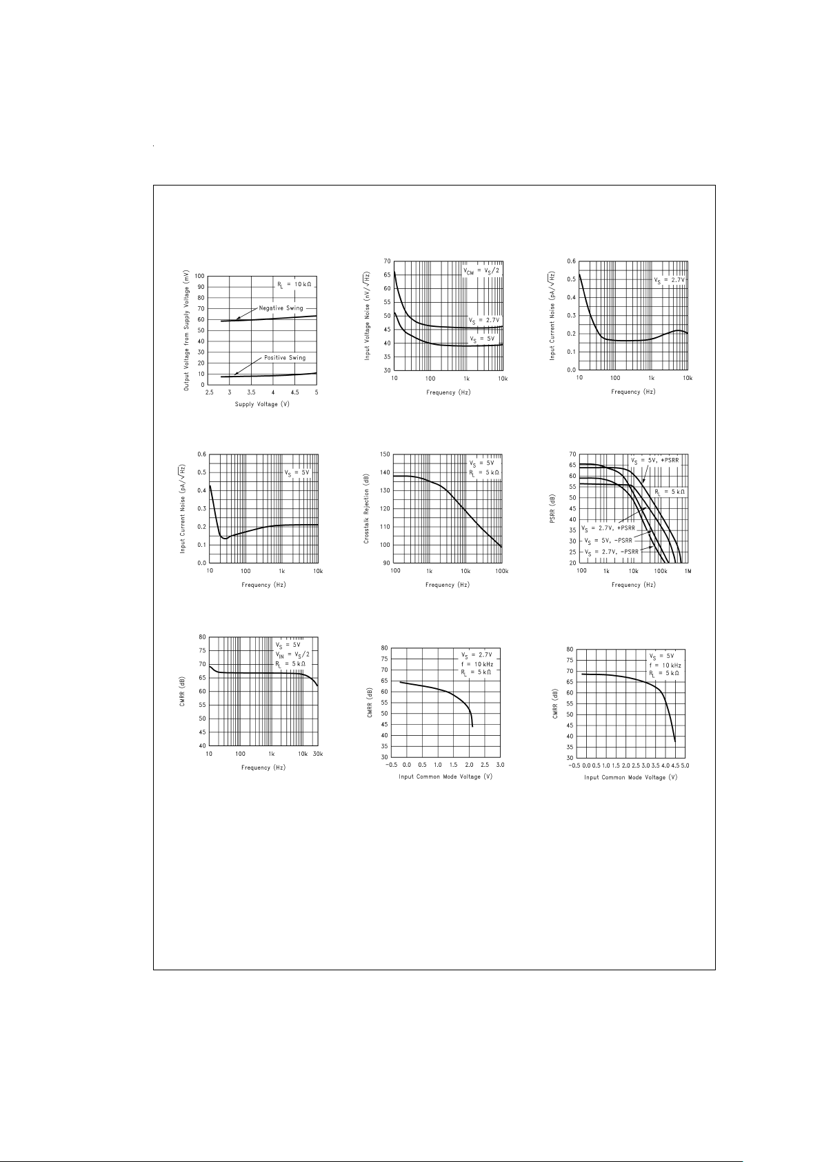
Typical Performance Characteristics Unless otherwise specified, V
S
= +5V, single supply,
T
A
= 25˚C. (Continued)
Output Voltage Swing
vs Supply Voltage
DS100060-67
Input Voltage Noise vs Frequency
DS100060-56
Input Current Noise vs Frequency
DS100060-60
Input Current Noise vs Frequency
DS100060-58
Crosstalk Rejection vs Frequency
DS100060-61
PSRR vs Frequency
DS100060-51
CMRR vs Frequency
DS100060-62
CMRR vs Input
Common Mode Voltage
DS100060-64
CMRR vs Input
Common Mode Voltage
DS100060-63
www.national.com 6
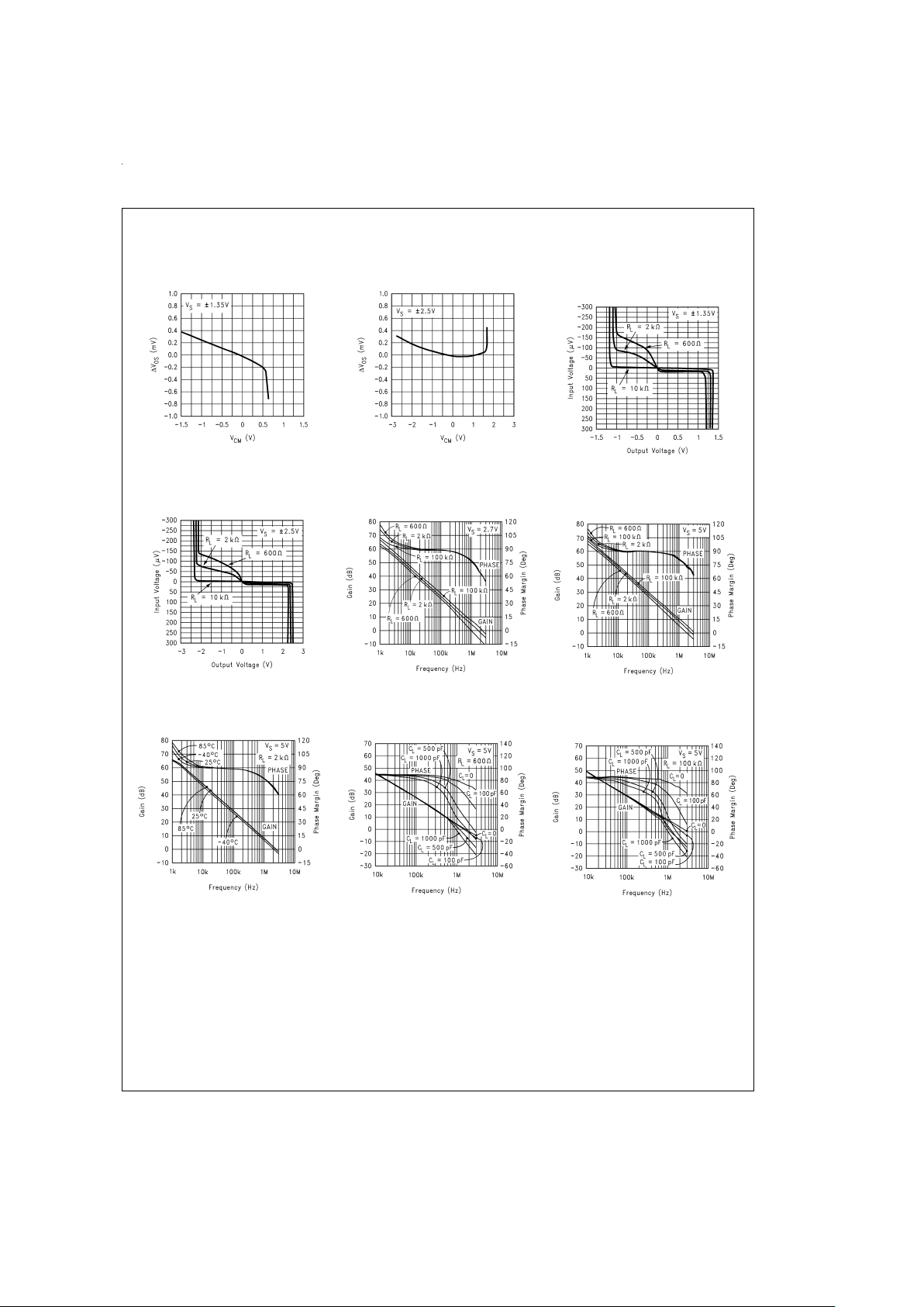
Typical Performance Characteristics Unless otherwise specified, V
S
= +5V, single supply,
T
A
= 25˚C. (Continued)
∆ V
OS
vs CMR
DS100060-53
∆ VOSvs CMR
DS100060-50
Input Voltage vs
Output Voltage
DS100060-54
Input Voltage vs
Output Voltage
DS100060-52
Open Loop
Frequency Response
DS100060-42
Open Loop
Frequency Response
DS100060-41
Open Loop Frequency
Response vs Temperature
DS100060-43
Gain and Phase vs
Capacitive Load
DS100060-45
Gain and Phase vs
Capacitive Load
DS100060-44
www.national.com7
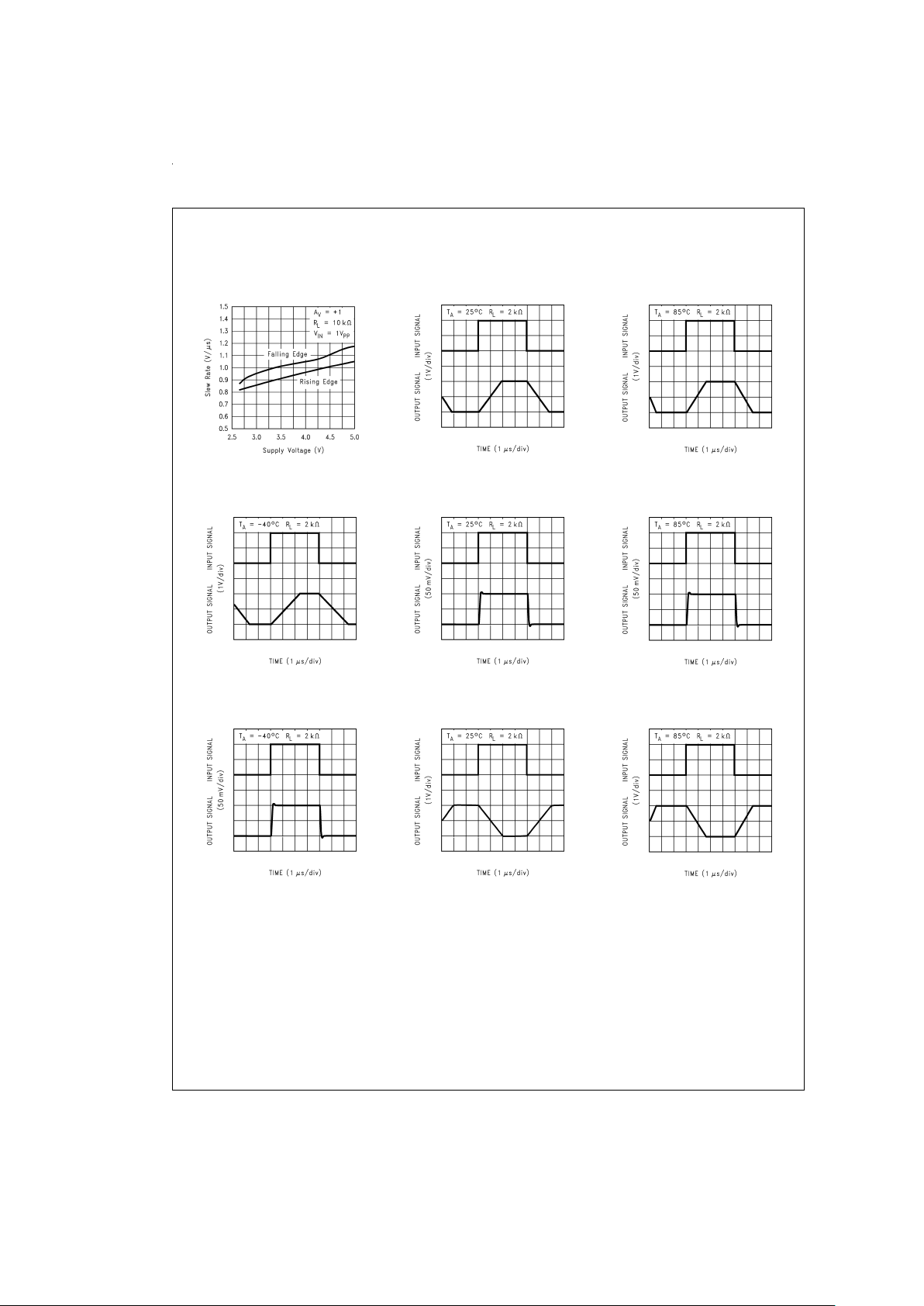
Typical Performance Characteristics Unless otherwise specified, V
S
= +5V, single supply,
T
A
= 25˚C. (Continued)
Slew Rate vs
Supply Voltage
DS100060-57
Non-Inverting Large
Signal Pulse Response
DS100060-88
Non-Inverting Large
Signal Pulse Response
DS100060-A1
Non-Inverting Large
Signal Pulse Response
DS100060-A0
Non-Inverting Small
Signal Pulse Response
DS100060-89
Non-Inverting Small
Signal Pulse Response
DS100060-A2
Non-Inverting Small
Signal Pulse Response
DS100060-A3
Inverting Large Signal
Pulse Response
DS100060-90
Inverting Large Signal
Pulse Response
DS100060-A4
www.national.com 8
 Loading...