December 2006
LMV221
50 MHz to 3.5 GHz 40 dB Logarithmic Power Detector for
CDMA and WCDMA
General Description
The LMV221 is a 40 dB RF power detector intended for use
in CDMA and WCDMA applications. The device has an RF
frequency range from 50 MHz to 3.5 GHz. It provides an accurate temperature and supply compensated output voltage
that relates linearly to the RF input power in dBm. The circuit
operates with a single supply from 2.7V to 3.3V.
The LMV221 has an RF power detection range from −45 dBm
to −5 dBm and is ideally suited for direct use in combination
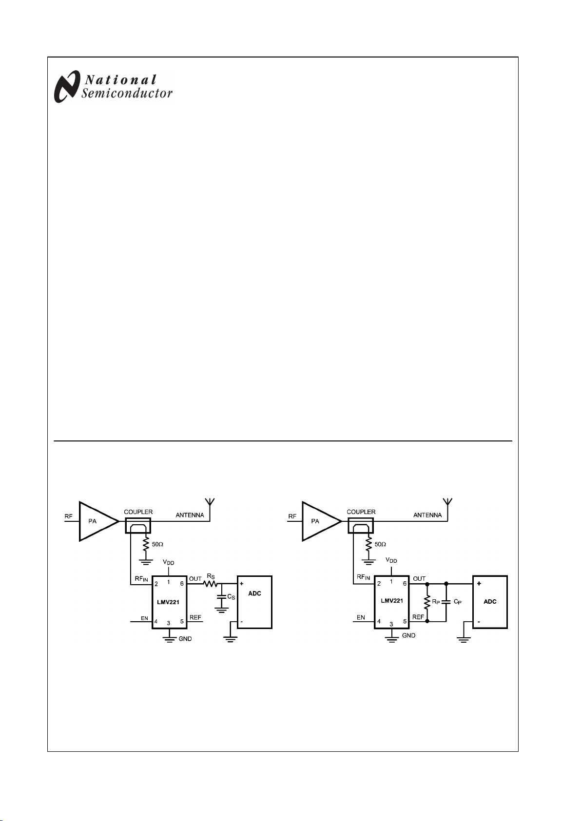
with a 30 dB directional coupler. Additional low-pass filtering
of the output signal can be realized by means of an external
resistor and capacitor. Figure (a) shows a detector with an
additional output low pass filter. The filter frequency is set with
RS and CS.
Figure (b) shows a detector with an additional feedback low
pass filter. Resistor RP is optional and will lower the Trans
impedance gain (R
TRANS
). The filter frequency is set with
CP//C
TRANS
and RP//R
TRANS
.
The device is active for Enable = High, otherwise it is in a low
power consumption shutdown mode. To save power and prevent discharge of an external filter capacitance, the output
(OUT) is high-impedance during shutdown.
The LMV221 power detector is offered in the small 2.2 mm x
2.5 mm x 0.8 mm LLP package.
Features
■
40 dB linear in dB power detection range
■
Output voltage range 0.3 to 2V
■
Shutdown
■
Multi-band operation from 50 MHz to 3.5 GHz
■
0.5 dB accurate temperature compensation
■
External configurable output filter bandwidth
■
2.2 mm x 2.5 mm x 0.8 mm LLP 6 package
Applications
■
UMTS/CDMA/WCDMA RF power control
■
GSM/GPRS RF power control
■
PA modules
■
IEEE 802.11b, g (WLAN)
Typical Application
(a) LMV221 with output RC Low Pass Filter
20173771
(b) LMV221 with feedback (R)C Low Pass Filter
20173704
© 2007 National Semiconductor Corporation 201737 www.national.com
LMV221 50 MHz to 3.5 GHz 40 dB Logarithmic Power Detector for CDMA and WCDMA

Absolute Maximum Ratings (Note 1)
If Military/Aerospace specified devices are required,
please contact the National Semiconductor Sales Office/
Distributors for availability and specifications.
Supply Voltage
VDD - GND
3.6V
RF Input
Input power 10 dBm
DC Voltage 400 mV
Enable Input Voltage VSS - 0.4V < V
EN
< VDD + 0.4V
ESD Tolerance (Note 2)
Human Body Model 2000V
Machine Model 200V
Charge Device Model 2000V
Storage Temperature
Range −65°C to 150°C
Junction Temperature
(Note 3) 150°C
Maximum Lead Temperature
(Soldering,10 sec) 260°C
Operating Ratings (Note 1)
Supply Voltage 2.7V to 3.3V
Temperature Range −40°C to +85°C
RF Frequency Range 50 MHz to 3.5 GHz
RF Input Power Range (Note 5) −45 dBm to −5 dBm
−58 dBV to −18 dBV
Package Thermal Resistance θ
JA
(Note 3) 86.6°C/W
2.7 V DC and AC Electrical Characteristics
Unless otherwise specified, all limits are guaranteed to; TA = 25°C, VDD = 2.7V, RF input frequency f = 1855 MHz CW (Continuous
Wave, unmodulated). Boldface limits apply at the temperature extremes (Note 4).
Symbol Parameter Condition Min
(Note 6)
Typ
(Note 7)
Max
(Note 6)
Units
Supply Interface
I
DD
Supply Current Active mode: EN = High, no Signal
present at RFIN.
6.5
5
7.2 8.5
10
mA
Shutdown: EN = Low, no Signal present
at RFIN.
0.5 3
4
μA
EN = Low: PIN = 0 dBm (Note 8) 10
Logic Enable Interface
V
LOW
EN Logic Low Input Level
(Shutdown mode)
0.6 V
V
HIGH
EN Logic High Input Level 1.1 V
I
EN
Current into EN Pin 1
μA
RF Input Interface
R
IN
Input Resistance 40 47.1 60
Ω
Output Interface
V
OUT
Output Voltage Swing From Positive Rail, Sourcing,
V
REF
= 0V, I
OUT
= 1 mA
16 40
50
mV
From Negative Rail, Sinking,
V
REF
= 2.7V, I
OUT
= 1 mA
14 40
50
I
OUT
Output Short Circuit Current Sourcing, V
REF
= 0V, V
OUT
= 2.6V 3
2.7
5.4
mA
Sinking, V
REF
= 2.7V, V
OUT
= 0.1V 3
2.7
5.7
BW Small Signal Bandwidth No RF input signal. Measured from REF
input current to V
OUT
450 kHz
R
TRANS
Output Amp Transimpedance
Gain
No RF Input Signal, from I
REF
to V
OUT
,
DC
35 42.7 55
kΩ
SR Slew Rate Positive, V
REF
from 2.7V to 0V 3
2.7
4.1
V/µs
Negative, V
REF
from 0V to 2.7V 3
2.7
4.2
R
OUT
Output Impedance
(Note 8)
No RF Input Signal, EN = High. DC
measurement
0.6 5
6
Ω
www.national.com 2
LMV221
Symbol Parameter Condition Min
(Note 6)
Typ
(Note 7)
Max
(Note 6)
Units
I
OUT,SD
Output Leakage Current in
Shutdown mode
EN = Low, V
OUT
= 2.0V 21 300
500
nA
RF Detector Transfer
V
OUT,MAX
Maximum Output Voltage
PIN= −5 dBm
(Note 8)
f = 50 MHz 1.67 1.76 1.83
V
f = 900 MHz 1.67 1.75 1.82
f = 1855 MHz 1.53 1.61 1.68
f = 2500 MHz 1.42 1.49 1.57
f = 3000 MHz 1.33 1.40 1.48
f = 3500 MHz 1.21 1.28 1.36
V
OUT,MIN
Minimum Output Voltage
(Pedestal)
No input Signal 175
142
250 350
388
mV
ΔV
OUT,MIN
Pedestal Variation over
temperature
No Input Signal, Relative to 25°C −20 20 mV
ΔV
OUT
Output Voltage Range
PIN from −45 dBm to −5 dBm
(Note 8)
f = 50 MHz 1.37 1.44 1.52
V
f = 900 MHz 1.34 1.40 1.47
f = 1855 MHz 1.24 1.30 1.37
f = 2500 MHz 1.14 1.20 1.30
f = 3000 MHz 1.07 1.12 1.20
f = 3500 MHz 0.96 1.01 1.09
K
SLOPE
Logarithmic Slope
(Note 8)
f = 50 MHz 39 40.5 42
mV/dB
f = 900 MHz 36.7 38.5 40
f = 1855 MHz 34.4 35.7 37.1
f = 2500 MHz 32.6 33.8 35.2
f = 3000 MHz 31 32.5 34
f = 3500 MHz 30 31.9 33.5
P
INT
Logarithmic Intercept
(Note 8)
f = 50 MHz −50.4 −49.4 −48.3
dBm
f = 900 MHz −54.1 −52.8 −51.6
f = 1855 MHz −53.2 −51.7 −50.2
f = 2500 MHz −51.8 −50 −48.3
f = 3000 MHz −51.1 −48.9 −46.6
f = 3500 MHz −49.6 −46.8 −44.1
t
ON
Turn-on Time
(Note 8)
No signal at PIN, Low-High transition
EN. V
OUT
to 90%
8 10
12
µs
t
R
Rise Time (Note 9) PIN = No signal to 0 dBm, V
OUT
from 10%
to 90%
2 12 µs
t
F
Fall Time (Note 9) PIN = 0 dBm to no signal, V
OUT
from 90%
to 10%
2 12 µs
e
n
Output Referred Noise
(Note 9)
PIN = −10 dBm, at 10 kHz 1.5
µV/
v
N
Output referred Noise
(Note 8)
Integrated over frequency band
1 kHz - 6.5 kHz
100 150
µV
RMS
PSRR Power Supply Rejection Ratio
(Note 9)
PIN = −10 dBm, f = 1800 MHz 55 60 dB
3 www.national.com
LMV221
Symbol Parameter Condition Min
(Note 6)
Typ
(Note 7)
Max
(Note 6)
Units
Power Measurement Performance
E
LC
Log Conformance Error
(Note 8)
−40 dBm ≤ PIN ≤ −10 dBm
f = 50 MHz −0.60
−1.10
0.53 0.56
1.3
dB
f = 900 MHz −0.70
−1.24
0.46 0.37
1.1
f = 1855 MHz −0.40
−1.1
0.48 0.24
1.1
f = 2500 MHz −0.43
−1.0
0.51 0.56
1.1
f = 3000 MHz −0.87
−1.2
0.56 1.34
1.6
f = 3500 MHz −1.73
−2.0
0.84 2.72
2.7
E
VOT
Variation over Temperature
(Note 8)
−40 dBm ≤ PIN ≤ −10 dBm
f = 50 MHz −1.1 0.4 1.4
dB
f = 900 MHz −1.0 0.38 1.27
f = 1855 MHz −1.1 0.44 1.31
f = 2500 MHz −1.1 0.48 1.15
f = 3000 MHz −1.2 0.5 0.98
f = 3500 MHz –1.2 0.62 0.85
E
1 dB
Measurement Error for a 1 dB
input power step (Note 8)
−40 dBm ≤ PIN ≤ −10 dBm
f = 50 MHz −0.06 0.069
dB
f = 900 MHz −0.056 0.056
f = 1855 MHz −0.069 0.069
f = 2500 MHz −0.084 0.084
f = 3000 MHz −0.092 0.092
f = 3500 MHz −0.10 0.10
E
10 dB
Measurement Error for a 10 dB
input power step (Note 8)
−40 dBm ≤ PIN ≤ −10 dBm
f = 50 MHz −0.65 0.57
dB
f = 900 MHz −0.75 0.58
f = 1855 MHz −0.88 0.72
f = 2500 MHz −0.86 0.75
f = 3000 MHz −0.85 0.77
f = 3500 MHz −0.76 0.74
S
T
Temperature Sensitivity
−40°C < TA < 25°C (Note 8)
−40 dBm ≤ PIN ≤ −10 dBm
f = 50 MHz −15 −7 1
mdB/°C
f = 900 MHz −13.4 −6 1.5
f = 1855 MHz −14.1 −5.9 2.3
f = 2500 MHz −13.4 −4.1 5.2
f = 3000 MHz −11.7 −1.8 8
f = 3500 MHz −10.5 0.5 1.2
S
T
Temperature Sensitivity
25°C < TA < 85°C (Note 8)
−40 dBm ≤ PIN ≤ −10 dBm
f = 50 MHz −12.3 −6.7 −1.1
mdB/°C
f = 900 MHz −13.1 −6.7 −0.2
f = 1855 MHz −14.7 −7.1 0.42
f = 2500 MHz −15.9 −7.6 0.63
f = 3000 MHz −18 −8.5 1
f = 3500 MHz −21.2 −9.5 2.5
S
T
Temperature Sensitivity
−40°C < TA < 25°C, (Note 8)
PIN = −10 dBm
f = 50 MHz −15.8 −8.3 −0.75
mdB/°C
f = 900 MHz −14.2 −6 2.2
f = 1855 MHz −14.9 −7.4 2
f = 2500 MHz −14.5 −6.6 1.3
f = 3000 MHz −13 −4.9 3.3
f = 3500 MHz −12 −3.4 5.3
www.national.com 4
LMV221
Symbol Parameter Condition Min
(Note 6)
Typ
(Note 7)
Max
(Note 6)
Units
S
T
Temperature Sensitivity
25°C < TA < 85°C, (Note 8)
PIN = −10 dBm
f = 50 MHz −12.4 −8.9 −5.3
mdB/°C
f = 900 MHz −13.7 −9.4 −5
f = 1855 MHz −14.6 −10 −5.6
f = 2500 MHz −15.2 −10.8 −6.5
f = 3000 MHz −16.5 −12.2 −7.9
f = 3500 MHz −18.1 −13.5 −9
P
MAX
Maximum Input Power for
ELC = 1 dB(Note 8)
f = 50 MHz −8.85 −5.9
dBm
f = 900 MHz −9.3 −6.1
f = 1855 MHz −8.3 −5.5
f = 2500 MHz −6 −4.2
f = 3000 MHz −5.4 −3.7
f = 3500 MHz −7.2 −2.7
P
MIN
Minimum Input Power for
ELC = 1 dB (Note 8)
f = 50 MHz −40.3 −38.9
dBm
f = 900 MHz −44.2 −42.9
f = 1855 MHz −42.9 −41.2
f = 2500 MHz −40.4 −38.6
f = 3000 MHz −38.4 −35.8
f = 3500 MHz −35.3 −31.9
DR Dynamic Range for ELC = 1 dB
(Note 8)
f = 50 MHz 31.5 34.5
dB
f = 900 MHz 34.4 38.1
f = 1855 MHz 34 37.4
f = 2500 MHz 33.8 36.1
f = 3000 MHz 32.4 34.8
f = 3500 MHz 26.2 32.7
Note 1: Absolute Maximum Ratings indicate limits beyond which damage to the device may occur. Operating Ratings indicate conditions for which the device is
intended to be functional, but specific performance is not guaranteed. For guaranteed specifications and the test conditions, see the Electrical Characteristics.
Note 2: Human body model, applicable std. MIL-STD-883, Method 3015.7. Machine model, applicable std. JESD22–A115–A (ESD MM std of JEDEC). FieldInduced Charge-Device Model, applicable std. JESD22–C101–C. (ESD FICDM std. of JEDEC)
Note 3: The maximum power dissipation is a function of T
J(MAX)
, θJA. The maximum allowable power dissipation at any ambient temperature is
PD = (T
J(MAX)
- TA)/θJA. All numbers apply for packages soldered directly into a PC board.
Note 4: Electrical Table values apply only for factory testing conditions at the temperature indicated. Factory testing conditions result in very limited self-heating
of the device such that TJ = TA. No guarantee of parametric performance is indicated in the electrical tables under conditions of internal self-heating where
TJ > TA.
Note 5: Power in dBV = dBm + 13 when the impedance is 50Ω.
Note 6: All limits are guaranteed by design or statistical analysis.
Note 7: Typical values represent the most likely parametric norm as determined at the time of characterization. Actual typical values may vary over time and will
also depend on the application and configuration. The typical values are not tested and are not guaranteed on shipped production material.
Note 8: All limits are guaranteed by design and measurements which are performed on a limited number of samples. Limits represent the mean ±3–sigma values.
The typical value represents the statistical mean value.
Note 9: This parameter is guaranteed by design and/or characterization and is not tested in production.
5 www.national.com
LMV221
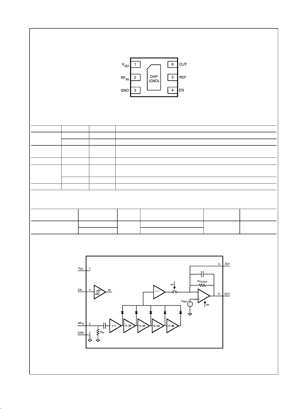
Connection Diagram
6-pin LLP
20173702
Top View
Pin Descriptions
LLP6 Name Description
Power Supply 1 V
DD
Positive Supply Voltage
3 GND Power Ground
Logic Input 4 EN The device is enabled for EN = High, and brought to a low-power shutdown mode for
EN = Low.
Analog Input 2 RF
IN
RF input signal to the detector, internally terminated with 50 Ω.
Output 5 REF Reference output, for differential output measurement (without pedestal). Connected to
inverting input of output amplifier.
6 OUT Ground referenced detector output voltage (linear in dB)
DAP GND Ground (needs to be connected)
Ordering Information
Package Part Number Package
Marking
Transport Media NSC Drawing Status
LLP-6
LMV221SD
A96
1k Units Tape and Reel
SDB06A Released
LMV221SDX 4.5k Units Tape and Reel
Block Diagram
20173703
LMV221
www.national.com 6
LMV221
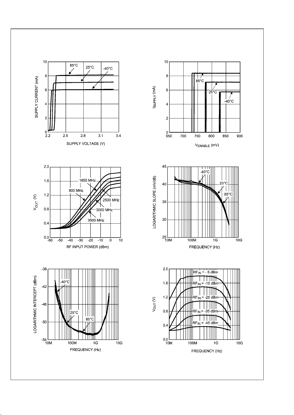
Typical Performance Characteristics Unless otherwise specified, V
DD
= 2.7V,
TA = 25°C, measured on a limited number of samples.
Supply Current vs. Supply Voltage
20173705
Supply Current vs. Enable Voltage
20173708
Output Voltage vs. RF input Power
20173712
Log Slope vs. Frequency
20173746
Log Intercept vs. Frequency
20173749
Output Voltage vs. Frequency
20173713
7 www.national.com
LMV221
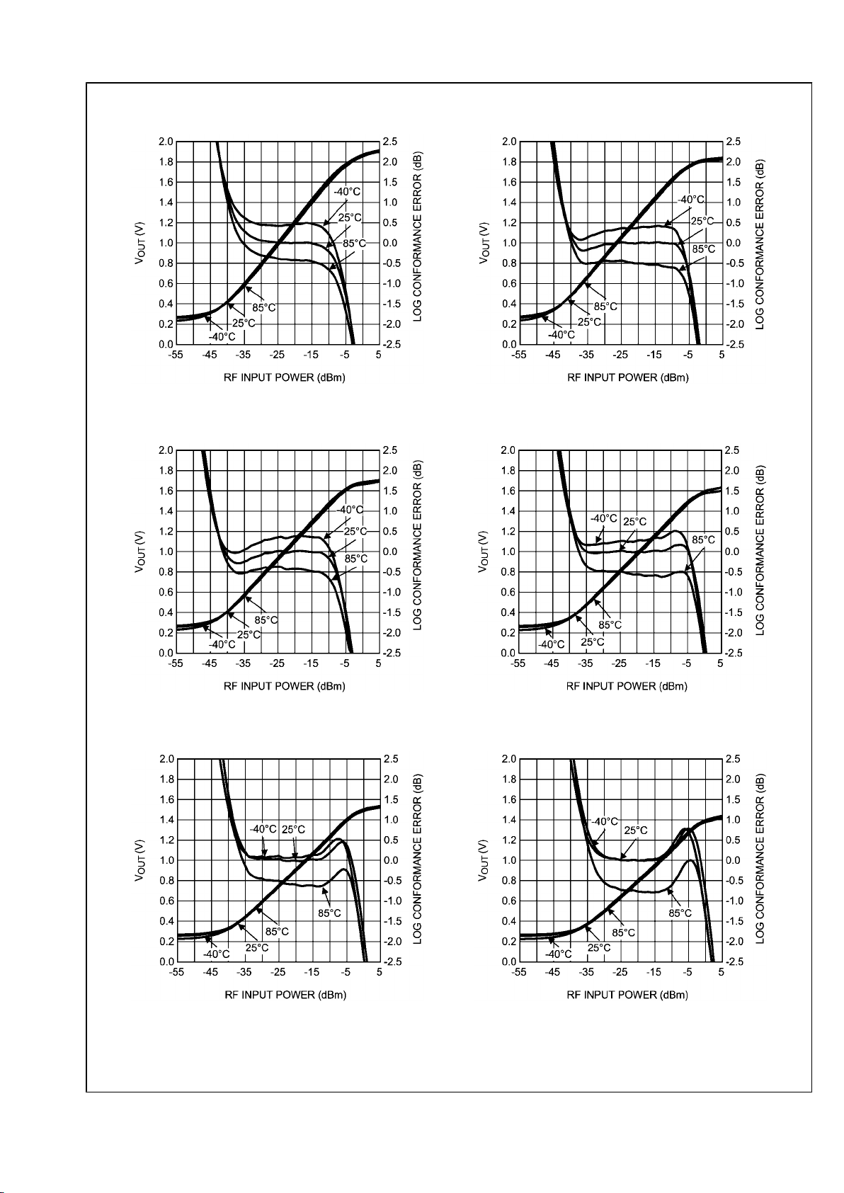
Mean Output Voltage and Log Conformance Error vs.
RF Input Power at 50 MHz
20173714
Mean Output Voltage and Log Conformance Error vs.
RF Input Power at 900 MHz
20173716
Mean Output Voltage and Log Conformance Error vs.
RF Input Power at 1855 MHz
20173715
Mean Output Voltage and Log Conformance Error vs.
RF Input Power at 2500 MHz
20173717
Mean Output Voltage and Log Conformance Error vs.
RF Input Power at 3000 MHz
20173718
Mean Output Voltage and Log Conformance Error vs.
RF Input Power at 3500 MHz
20173719
www.national.com 8
LMV221
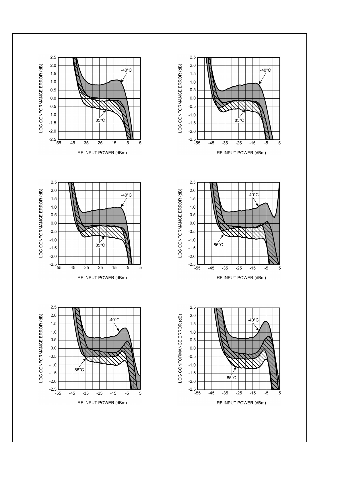
Log Conformance Error (Mean ±3 sigma) vs.
RF Input Power at 50 MHz
20173762
Log Conformance Error (Mean ±3 sigma) vs.
RF Input Power at 900 MHz
20173763
Log Conformance Error (Mean ±3 sigma) vs.
RF Input Power at 1855 MHz
20173764
Log Conformance Error (Mean ±3 sigma) vs.
RF Input Power at 2500 MHz
20173768
Log Conformance Error (Mean ±3 sigma) vs.
RF Input Power at 3000 MHz
20173769
Log Conformance Error (Mean ±3 sigma) vs.
RF Input Power at 3500 MHz
20173767
9 www.national.com
LMV221
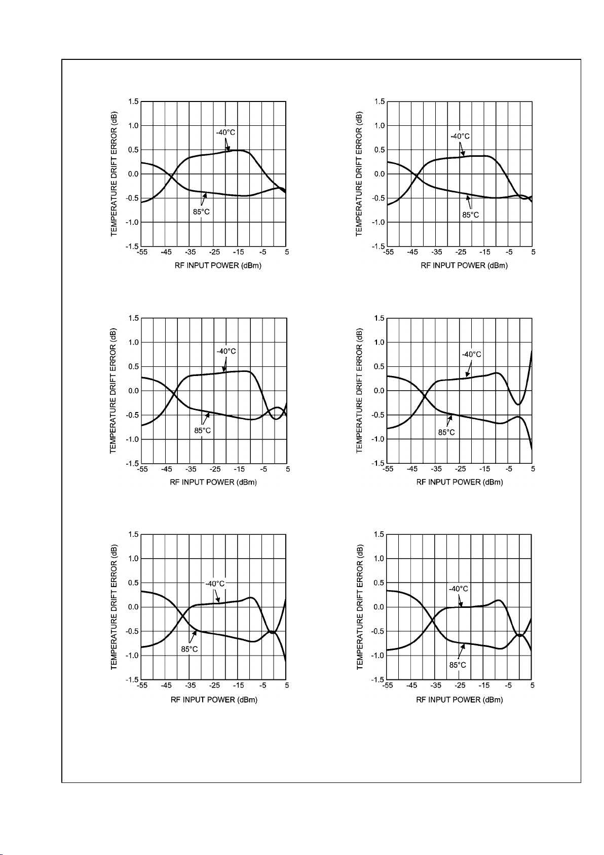
Mean Temperature Drift Error vs.
RF Input Power at 50 MHz
20173720
Mean Temperature Drift Error vs.
RF Input Power at 900 MHz
20173721
Mean Temperature Drift Error vs.
RF Input Power at 1855 MHz
20173722
Mean Temperature Drift Error vs.
RF Input Power at 2500 MHz
20173723
Mean Temperature Drift Error vs.
RF Input Power at 3000 MHz
20173724
Mean Temperature Drift Error vs.
RF Input Power at 3500 MHz
20173725
www.national.com 10
LMV221
 Loading...