NSC LMV1088RL, LMV1088 Datasheet
March 28, 2008
LMV1088
Dual Input, Far Field Noise Suppression Microphone
Amplifier with Automatic Calibration Ability
General Description
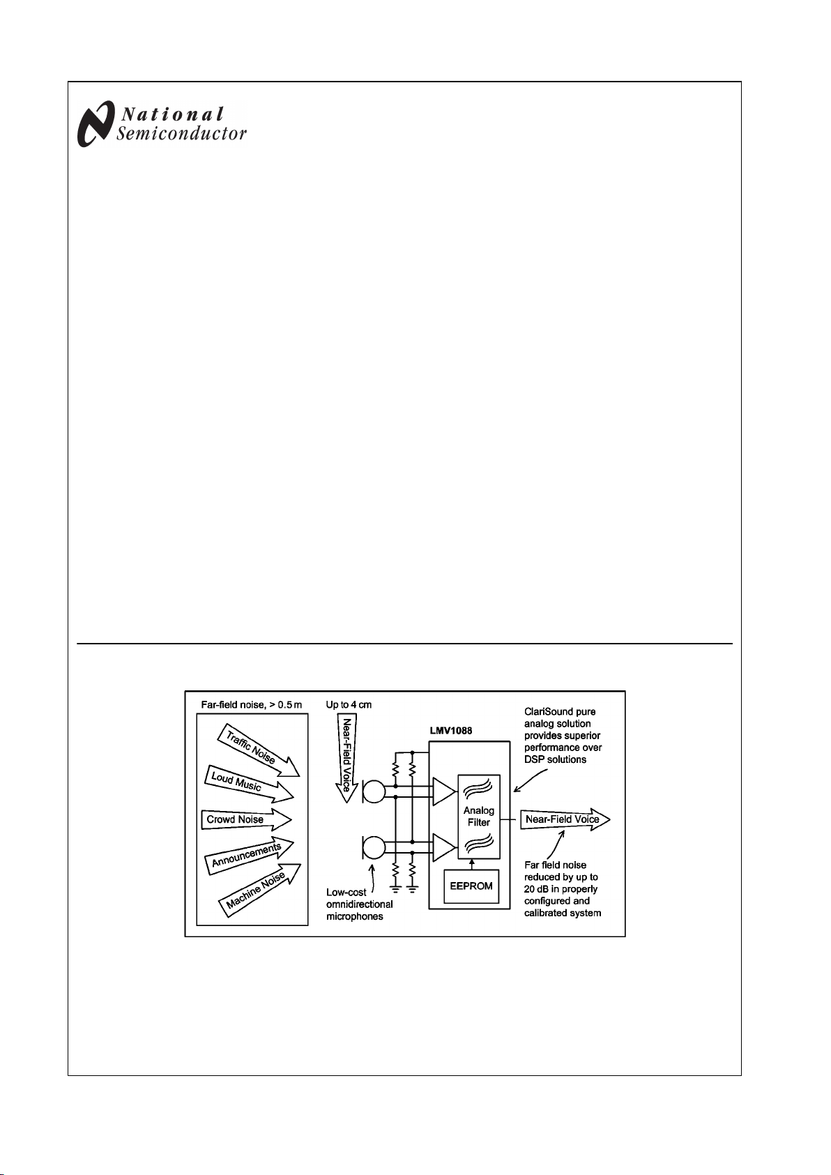
The LMV1088 amplifies near-field voice signals within 4cm of
the microphones while rejecting far-field acoustic noise
greater than 0.5m from the microphones. Up to 20dB of farfield rejection is possible in a properly configured and calibrated system.
Part of the Powerwise® family of energy efficient solutions,
the LMV1088 consumes 1mA of supply current while providing superior performance to DSP solutions consuming over
10 times the power.
A fast calibration during the manufacturing test process allows the LMV1088 to compensate the entire microphone
system. This calibration includes mismatch in microphone
gain and frequency response, as well as acoustical path variances. The LMV1088 stores the calibration coefficients in onboard EEPROM. The calibration is initiated by I2C command
or by pin control.
The dual microphone inputs are differential to provide excellent noise immunity. The microphones are biased with an
internal low-noise bias supply.
Key Specifications
(3.3V supply, unless otherwise specified)
■
Supply voltage 2.7V to 5.5V
■
Supply current 1mA (typ)
■
Signal to noise ratio (A-weighted) 60dB (typ)
■
Total harmonic distortion (A-weighted) 0.1% (typ)
■
Noise cancellation 20dB (typ)
■
PSRR 85dB (typ)
Features
■
Low power consumption
■
No added processing delay
■
Automatic Calibration
■
Space-saving 36 Bump micro SMD package
■
Up to 20dB SNRI
Applications
■
Mobile handsets
■
Mobile and handheld two-way radios
■
Bluetooth and other powered headsets
■
Hand-held voice microphones
■
Portable public address systems
Application of the LMV1088
20213028
PowerWise® is a registered trademark of National Semiconductor Corporation.
© 2008 National Semiconductor Corporation 202130 www.national.com
LMV1088 Dual Input, Far Field Noise Suppression Microphone Amplifier with Automatic
Calibration Ability
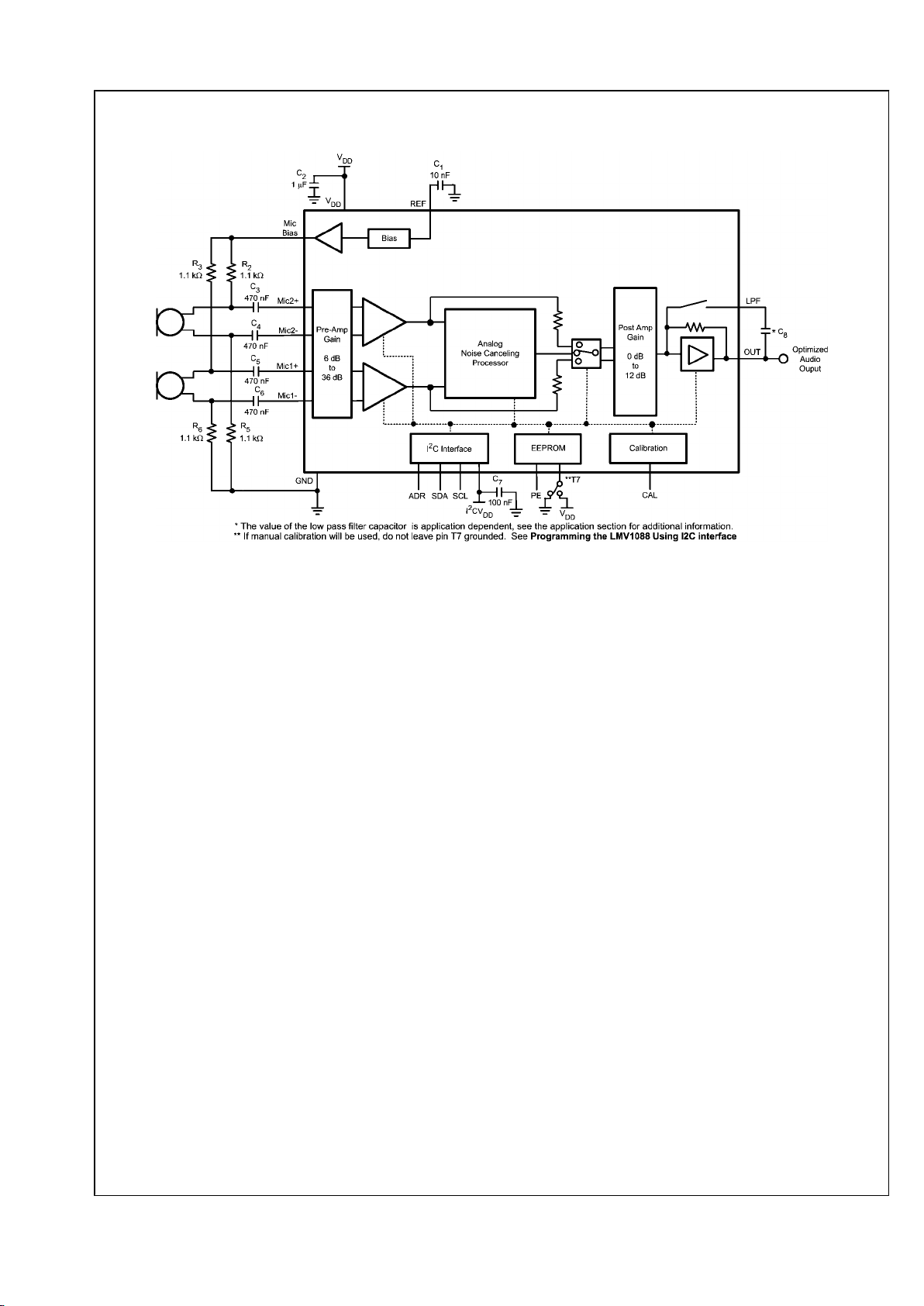
Typical Application
20213041
FIGURE 1. Typical Dual Microphone Far Field noise Cancelling Application
www.national.com 2
LMV1088
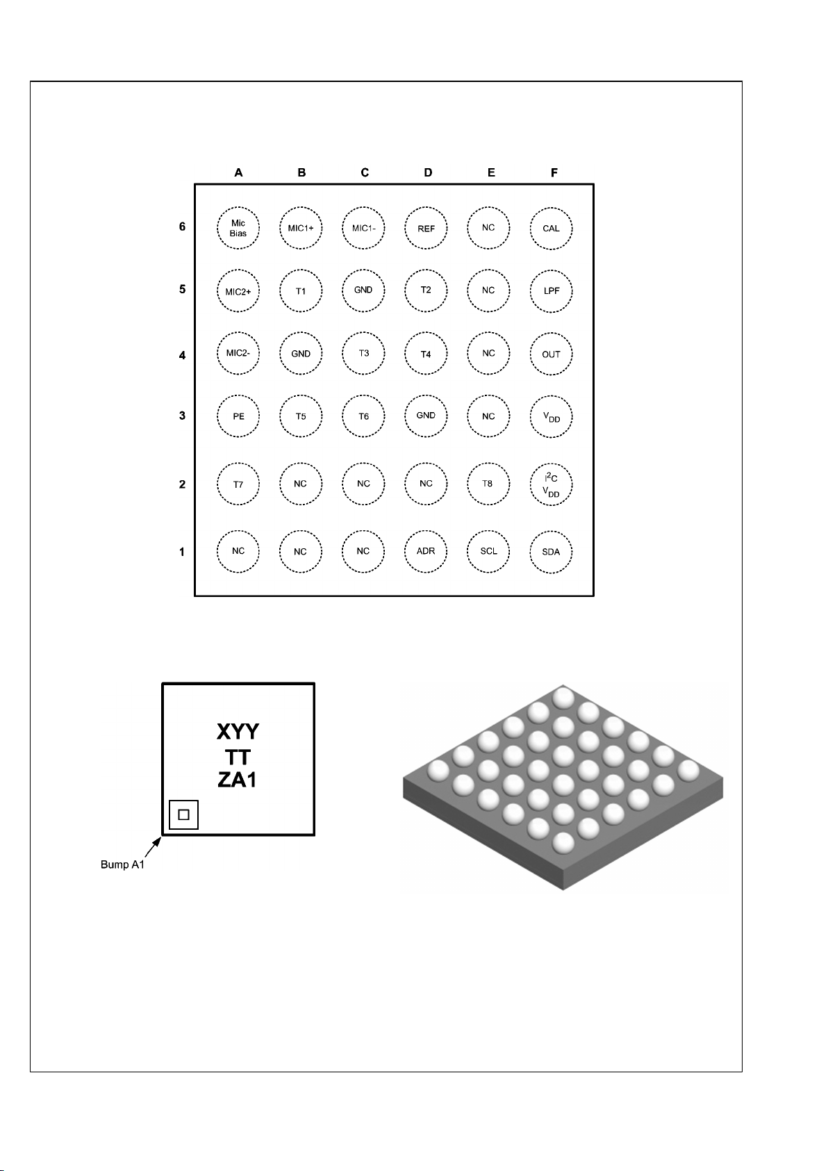
Connection Diagrams
36 Bump micro SMD package
20213030
Top View
Order Number LMV1088RL
See NS Package Number RLA36TTA
36 Bump micro SMD Marking
20213031
Top View
X = Plant Code
YY = Date Code
TT= Die Tracability
ZA1 = LMV1088RL
micro SMD Package View
20213033
Bottom View
3 www.national.com
LMV1088
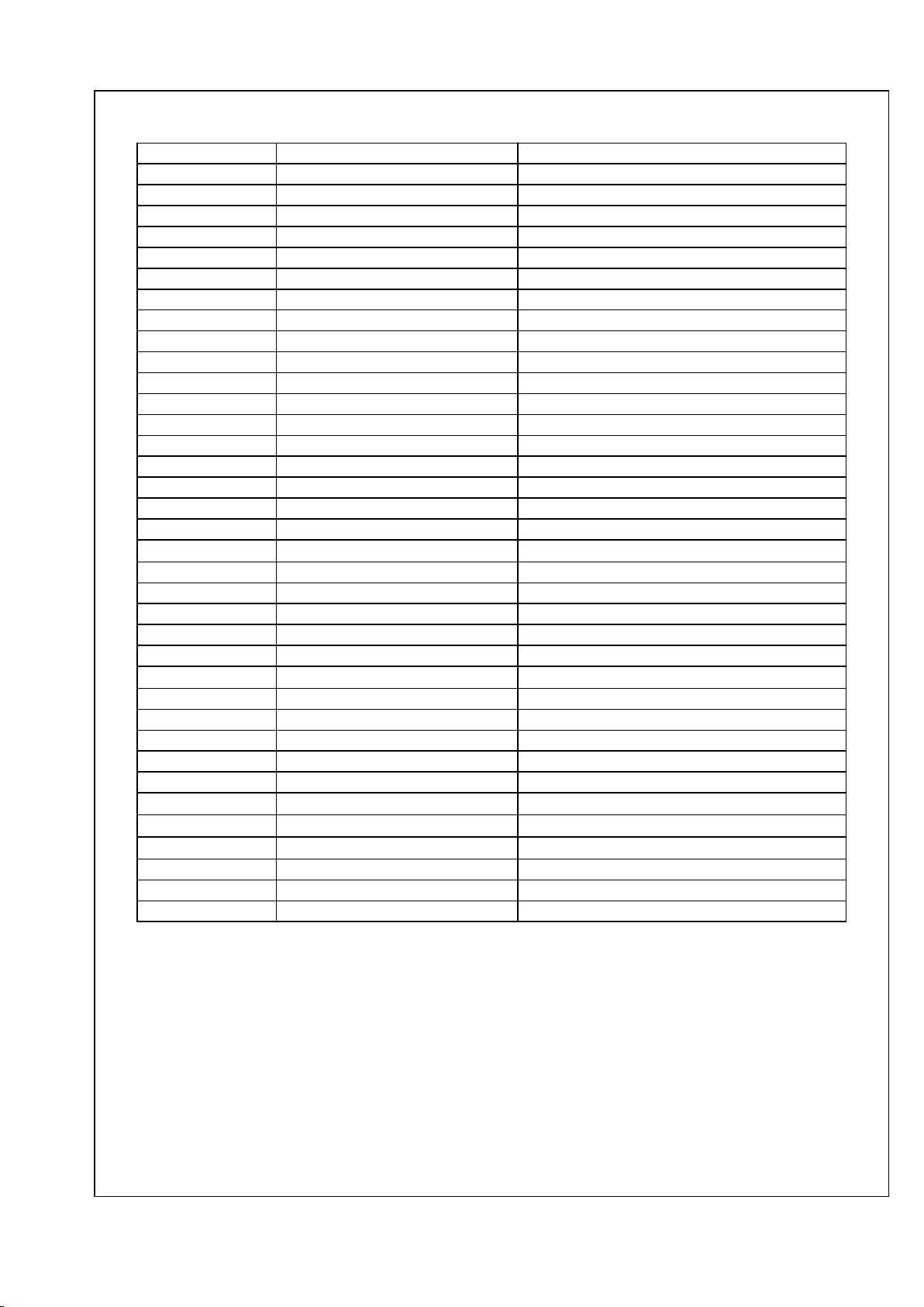
TABLE 1. Pin Name and Function
Bump Number Pin Name Pin Function
A1 NC No Connect (Note 1)
A2 T7 Control pin (Note 3)
A3 PE Program Enable EEPROM
A4 MIC2– microphone 2 input —
A5 MIC2+ microphone 2 input +
A6 Mic Bias Bias for Microphones
B1 NC No Connect (Note 1)
B2 NC No Connect (Note 1)
B3 T5 Float(Note 2)
B4 GND Amplifier ground
B5 T1 Float(Note 2)
B6 MIC1+ microphone 1 input +
C1 NC No Connect (Note 1)
C2 NC No Connect (Note 1)
C3 T6 Float(Note 2)
C4 T3 Float(Note 2)
C5 GND Amplifier ground
C6 MIC1– microphone 1 input —
D1 ADR I2C Address select
D2 NC No Connect (Note 1)
D3 GND Amplifier ground
D4 T4 Float(Note 2)
D5 T2 Connect to GND
D6 REF Reference Voltage De-coupling
E1 SCL I2C Clock
E2 T8 Connect to GND
E3 NC No Connect (Note 1)
E4 NC No Connect (Note 1)
E5 NC No Connect (Note 1)
E6 NC No Connect (Note 1)
F1 SDA I2C Data
F2 I2CV
DD
I2C power supply
F3 V
DD
Power Supply
F4 OUT Optimized Audio Out
F5 LPF Lowpasss Filter Capacitor
F6 CAL Calibration Start
Note 1: Connect NC pins to GND for optimum noise performance.
Note 2: Do not ground pins.
Note 3: Force VDD setup for manual calibrations. Force GND setup for calibration circuitry.
www.national.com 4
LMV1088

Absolute Maximum Ratings (Note 4)
If Military/Aerospace specified devices are required,
please contact the National Semiconductor Sales Office/
Distributors for availability and specifications.
Supply Voltage 6.0V
Storage Temperature -85°C to +150°C
ESD Rating (Note 7) 2000V
ESD Rating (Note 8) 200V
Junction Temperature (T
JMAX
) 150°C
Mounting Temperature
Infrared or Convection (20 sec.)
235°C
Thermal Resistance
θJA (microSMD)
70°C/W
Soldering Information See AN-112 “microSMD Wafers Level
Chip Scale Package.”
Operating Ratings (Note 5)
Supply Voltage 2.7V to 5.5V
I2CVDD (Note 13) 1.8V to 5.5V
Temperature Range −40°C to 85°C
Electrical Characteristics 3.3V (Note 4)
Unless otherwise specified, all limits guaranteed for TJ = 25°C, VDD = 3.3V, VIN = 18mVPP, pass through mode (Note 11), preamplifier
gain = 20dB, postamplifier gain = -2.5dB, RL = 100kΩ, and CL = 4.7pF.
Symbol Parameter Conditions
LMV1088
Units (Limits)
Typical (Note 9) Limits (Note 10)
SNR
Signal-to-Noise Ratio f = 1kHz, , V
IN
= 18mVPP, A-Weighted 60 dB
VINMax Input Signal f = 1kHz and THD+N < 1% 97 mV
PP
V
out
AC Output Voltage f = 1kHz 500 mV
RMS
DC Output Voltage 800 mV
THD+N
Total Harmonic Distortion + Noise f = 1kHz, VIN = 18mV
PP
0.1 %
Z
IN
Input Impedance 100
kΩ
Z
OUT
Output Impedance 150
Ω
Z
LOAD
R
LOAD
C
LOAD
10
10
kΩ (min)
pF (max)
AMMicrophone Pre Amplifier Gain Range f = 1kHz 6 – 36 dB
A
MR
Microphone Pre Amplifier Gain
Adjustment Resolution
f = 1kHz 2 dB
A
P
Post Amplifier Gain Range
f = 1kHz Pass Through Mode and
Summing Mode
-2.5 – 9.5 dB
f = 1kHz Noise Canceling Mode
(Note 12)
0 – 12 dB
A
PR
Post Amplifier Gain Adjustment
Resolution
f = 1kHz 3 dB
A
CR
Gain Compensation Range
f = 300Hz — f = 3400Hz ±3 dB (max)
A
MD
Gain Matching Difference After
Calibration
f = 300Hz
f = 1kHz
f = 3kHz
0.5
0.5
0.5
dB (max)
dB (max)
dB (max)
T
CAL
Calibration Duration 770 ms (max)
PSRR Power Supply Rejection Ratio
Input Referred, Input AC grounded
f = 217Hz (100mVPP) 85 dB
f = 1kHz (100mVPP) 80 dB
CMRR Common Mode Rejection Ratio f = 1kHz, 60 dB
VBMMicrophone Bias Supply Voltage I
BIAS
= 1mA 2.0 V
ε
VBM
Microphone Bias Supply Noise A-Weighted 10
μV
RMS
I
BM
Total available Microphone Bias
Current
1.2 mA (min)
I
DDQ
Supply Quiescent Current VIN = 0V
1 1.5 mA (max)
I
DDCP
Supply Current during Calibration and
Programming
Calibrating or Programming
EEPROM
28 50 mA (max)
I
DD
Supply Current
Vin = 25mVPP both inputs, Noise
canceling mode
1 1.5 mA (max)
5 www.national.com
LMV1088

Digital Interface Characteristics (Notes 4, 13)
Unless otherwise specified, all limits guaranteed for TJ = 25°C, I2CVDD within the Operating Rating (Note 13)
Symbol Parameter Conditions
LMV1088
Units
(Limits)
Typical
(Note 9)
Limits (Note
10)
V
IH
Logic High Input Level SCL, SDA, ADR, CAL, PE pins
0.6xI2CV
DD
V (min)
V
IL
Logic Low Input Level SCL, SDA, ADR, CAL, PE pins
0.4xI2CV
DD
V (max)
ts
CAL
CAL Setup Time 2 ms
th
CAL
CAL Hold time until calibration is
finished
770 ms (min)
ts
PEC
PE Setup Time 2 ms
th
PEC
PE Hold until calibration is finished 770 ms (min)
Note 4: “Absolute Maximum Ratings” indicate limits beyond which damage to the device may occur, including inoperability and degradation of device reliability
and/or performance. Functional operation of the device and/or non-degradation at the Absolute Maximum Ratings or other conditions beyond those indicated in
the Recommended Operating Conditions is not implied. The Recommended Operating Conditions indicate conditions at which the device is functional and the
device should not be operated beyond such conditions. All voltages are measured with respect to the ground pin, unless otherwise specified.
Note 5: The Electrical Characteristics tables list guaranteed specifications under the listed Recommended Operating Conditions except as otherwise modified
or specified by the Electrical Characteristics Conditions and/or Notes. Typical specifications are estimations only and are not guaranteed.
Note 6: The maximum power dissipation must be de-rated at elevated temperatures and is dictated by T
JMAX
, θJC, and the ambient temperature TA. The maximum
allowable power dissipation is P
DMAX
= (T
JMAX
–TA)/ θJA or the number given in the Absolute Maximum Ratings, whichever is lower. For the LMV1088, T
JMAX
=
150°C and the typical θJA for this microSMD package is 70°C/W and for the LLP package θJA is 64°C/W Refer to the Thermal Considerations section for more
information.
Note 7: Human body model, applicable std. JESD22-A114C.
Note 8: Machine model, applicable std. JESD22-A115-A.
Note 9: Typical values represent most likely parametric norms at TA = +25°C, and at the Recommended Operation Conditions at the time of product
characterization and are not guaranteed.
Note 10: Datasheet min/max specification limits are guaranteed by test, or statistical analysis.
Note 11: In Pass Through mode, only one microphone input is active. See also I2C Compatible Interface for more information how to configure the LMV1088.
Note 12: In Noise Canceling Mode there is 2.5dB additional gain before calibration when compared to the other operating modes to compensate for the gain
reduction that is caused by the noise canceling effect.
Note 13: The voltage at I2CVDD must not exceed the voltage on VDD.
www.national.com 6
LMV1088
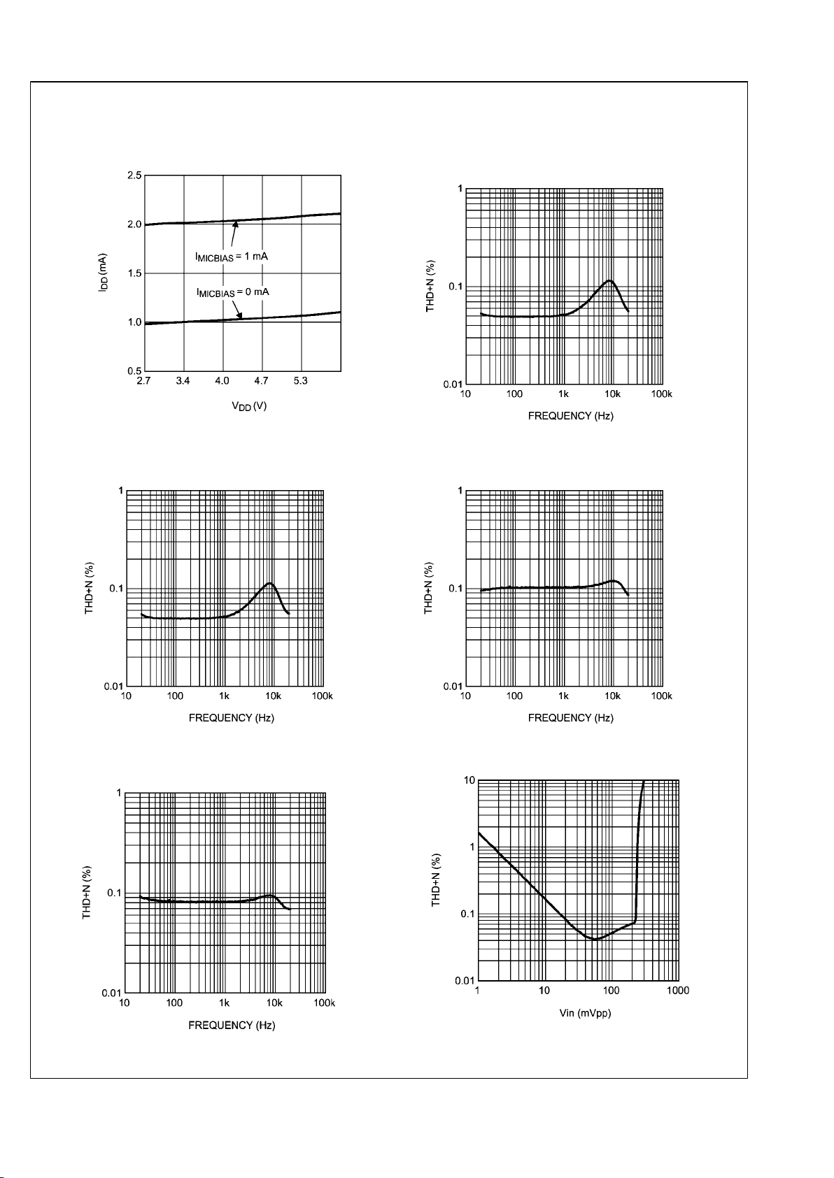
Typical Performance Characteristics Unless otherwise specified, T
J
= 25°C, VDD = 3.3V, VIN =
18mVPP, pass through mode (Note 11), preamplifier gain = 20dB, postamplifier gain = –2.5dB, RL = 100kΩ, and CL = 4.7pF.
Supply Current vs. Supply Voltage
20213021
THD+N vs Frequency, pass through mode Mic1
VIN = 36mV
pp
20213003
THD+N vs Frequency, pass through mode Mic2
VIN = 36mV
pp
20213004
THD+N vs Frequency, Noise canceling mode
signal at Mic1, Mic2 AC shorted, VIN = 36mV
pp
20213005
THD+N vs Frequency, Noise canceling mode
Mic1 AC shorted, signal at Mic2, VIN = 36mV
pp
20213006
THD+N vs Vin, pass through mode Mic1
20213016
7 www.national.com
LMV1088
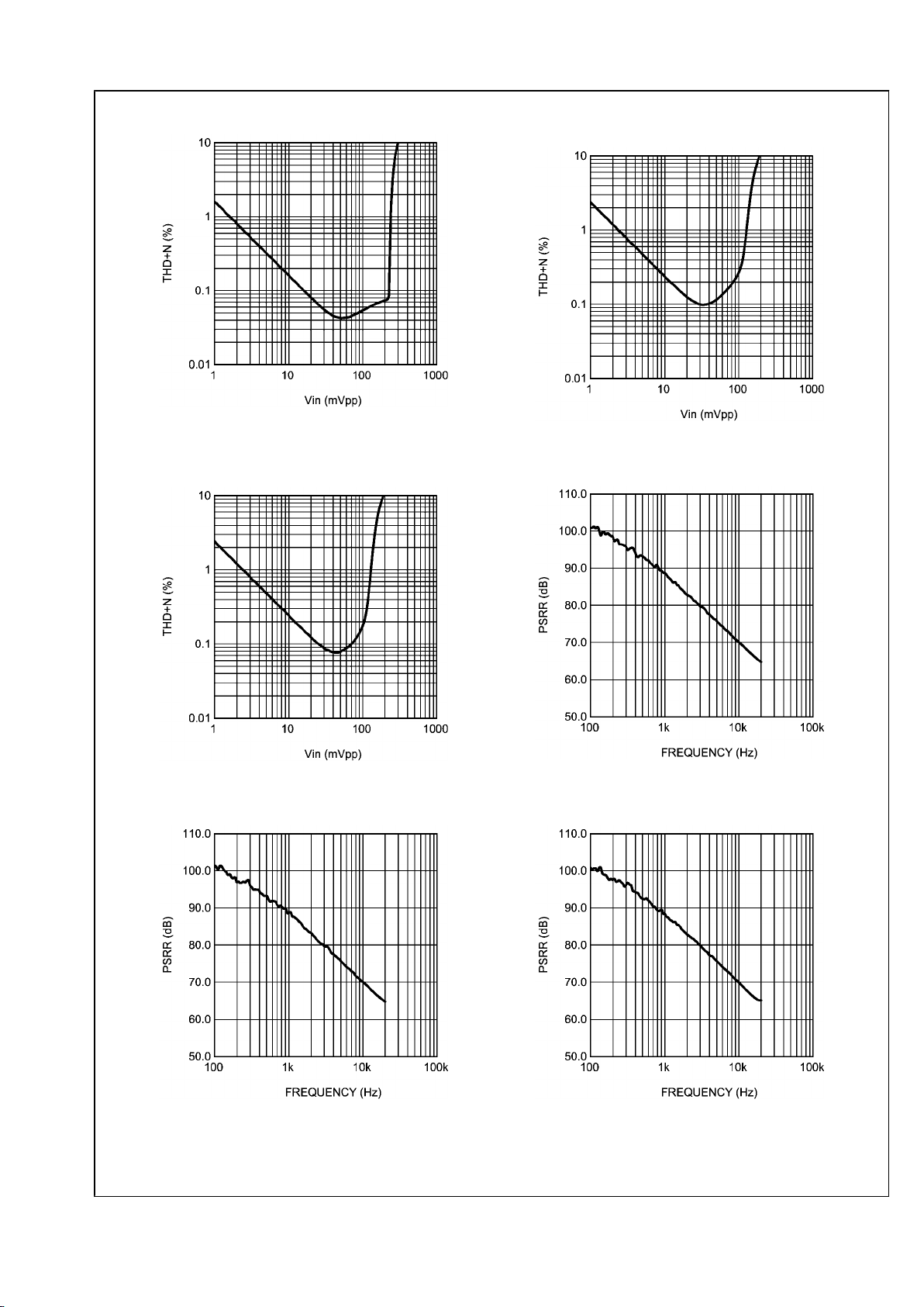
THD+N vs Vin, pass through mode Mic2
20213015
THD+N vs Vin, Noise canceling mode
signal at Mic1, Mic2 AC shorted
20213014
THD+N vs Vin, Noise canceling mode
Mic1 AC shorted, signal at Mic2
20213017
PSRR vs Frequency, pass through mode Mic1,
Mic1+ Mic2 AC shorted
20213018
PSRR vs Frequency, pass through mode Mic2,
Mic1+ Mic2 AC shorted
20213019
PSRR vs Frequency, Noise canceling mode ,
Mic1+ Mic2 AC shorted
20213020
www.national.com 8
LMV1088
 Loading...