

NSC LMV1012TPX-15, LMV1012TPX-07, LMV1012TP-15, LMV1012UP-15, LMV1012TPX-25 Datasheet
...
May 2003
LMV1012-07/ LMV1012-15/ LMV1012-25
Analog Pre-Amplified IC’s for High Gain Microphones
LMV1012-07/ LMV1012-15/ LMV1012-25 Analog Amplifier IC for High Gain Microphones
General Description
The LMV1012 is an audio amplifier series for small form
factor electret microphones. It is designed to replace the
JFET amplifier currently being used. The LMV1012 series is
ideally suited for applications requiring high signal integrity in
the presence of ambient or RF noise, such as in cellular
communications. The LMV1012 audio amplifiers are guaranteed to operate over a 2.2V to 5.0V supply voltage range
with fixed gains of 7.8dB, 15.6dB and 23.8dB. The devices
offer excellent gain accuracy and temperature stability as
compared to a JFET microphone.
The LMV1012 series enables a two-pin electret microphone
solution, which provides direct pin-to-pin compatibility with
the existing JFET market.
The devices are offered in two space saving 4-bump micro
™
SMD
and LMV1012TP-25 are well suited for canister packages
1.8mm and thicker. The LMV1012UP-15 is ideal for canisters
1.3mm and thicker. These miniature packages are designed
for electret condenser microphones (ECM) form factor.
packages. The LMV1012TP-07, LMV1012TP-15,
Features
(Typical LMV1012-15, 2.2V supply, RL= 2.2kΩ, C = 2.2µF,
= 18mVPP, unless otherwise specified)
V
IN
n Supply voltage 2V - 5V
n Supply current
n Signal to noise ratio (A-weighted) 60dB
n Output voltage noise (A-weighted) −89dBV
n Total Harmonic Distortion 0.09%
n Voltage gain
— LMV1012-07 7.8dB
— LMV1012-15 15.6dB
— LMV1012-25 23.8dB
n Temperature range −40˚C to 85˚C
n Offered in 4-bump micro SMD packages:
— 0.93 x 1.0 x 0.4mm
— 0.93 x 1.0 x 0.5mm
<
180µA
Applications
n Cellular phones
n Headsets
n Mobile communications
n Automotive accessories
n PDAs
n Accessory microphone products
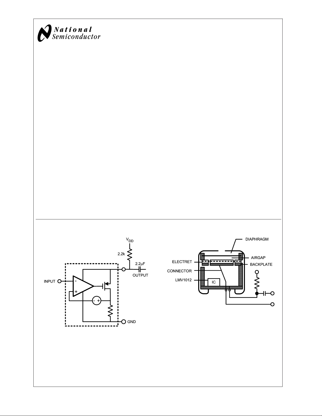
Schematic Diagram
Built-In Gain Electret Microphone
20072302
20072301
© 2003 National Semiconductor Corporation DS200723 www.national.com
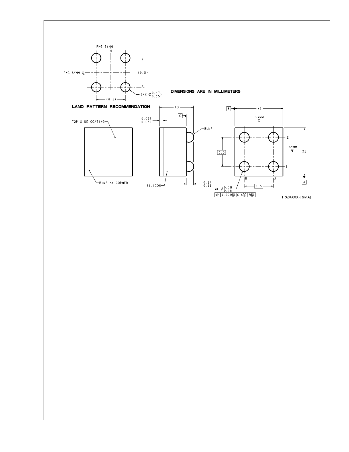
Physical Dimensions inches (millimeters)
unless otherwise noted
LMV1012-07/ LMV1012-15/ LMV1012-25
NOTE: UNLESS OTHERWISE SPECIFIED.
1. EPOXY COATING.
2. 63Sn/37Pb EUTECTIC BUMP.
3. RECOMMEND NON-SOLDER MASK DEFINED LANDING PAD.
4. PIN A1 IS ESTABLISHED BY LOWER LEFT CORNER WITH RESPECT TO TEXT ORIENTATION PINS ARE NUMBERED COUNTERCLOCKWISE.
5. XXX IN DRAWING NUMBER REPRESENTS PACKAGE SIZE VARIATION WHERE X1 IS PACKAGE WIDTH, X2 IS PACKAGE LENGTH AND X3 IS
PACKAGE HEIGHT.
6. REFERENCE JEDEC REGISTRATION MO-211. VARIATION BC.
4-Bump Thin micro SMD
NS Package Number TPA04GKA
= 0.93mm X2= 1.006mm X3= 0.500mm
X
1
www.national.com 2
 Loading...