

NSC LMC7101AIM5X, LMC7101AIM5, LMC7101BIN, LMC7101BIM5X, LMC7101BIM5 Datasheet
LMC7101
Tiny Low Power Operational Amplifier with Rail-To-Rail
Input and Output
General Description
The LMC7101 is a high performance CMOS operational amplifier available in the space saving SOT 23-5 Tiny package.
This makes the LMC7101 ideal for space and weight critical
designs. The performance is similar to a single amplifier of
the LMC6482/4 type, with rail-to-rail input and output, high
open loop gain, low distortion, and low supply currents.
The main benefits of the Tiny package are most apparent in
small portable electronic devices, such as mobile phones,
pagers, notebook computers, personal digital assistants,
and PCMCIA cards. The tiny amplifiers can be placed on a
board where they are needed, simplifying board layout.
Features
n Tiny SOT23-5 package saves space —typical circuit
layouts take half the space of SO-8 designs
n Guaranteed specs at 2.7V, 3V, 5V, 15V supplies
n Typical supply current 0.5 mA at 5V
n Typical total harmonic distortion of 0.01%at 5V
n 1.0 MHz gain-bandwidth
n Similar to popular LMC6482/4
n Input common-mode range includes V
−
and V
+
n Tiny package outside dimensions—120 x 118 x 56 mils,
3.05 x 3.00 x 1.43 mm
Applications
n Mobile communications
n Notebooks and PDAs
n Battery powered products
n Sensor interface
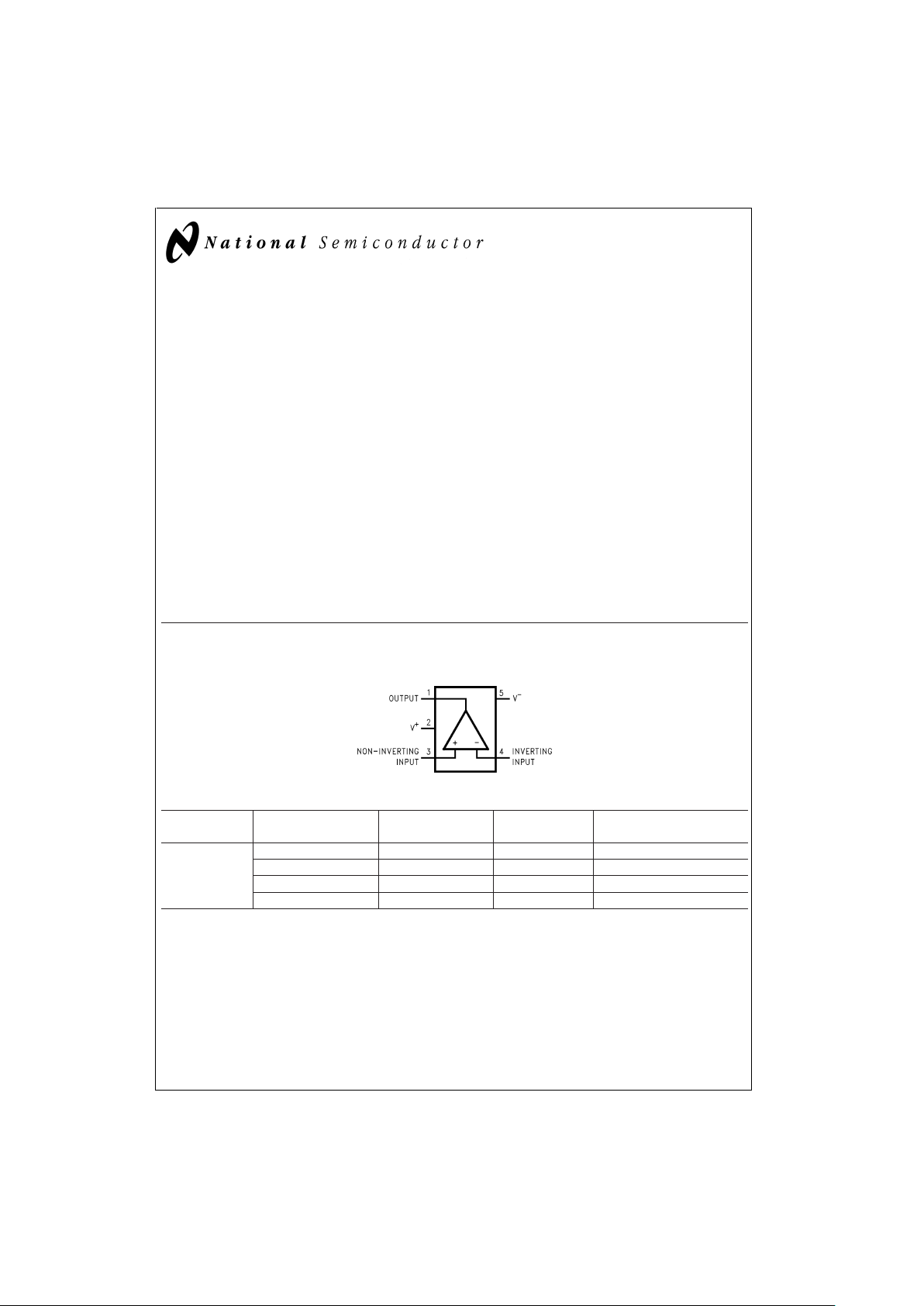
Connection Diagram
Package Ordering Information NSC Drawing
Number
Package
Marking
Supplied As
5-Pin SOT 23-5
LMC7101AIM5 MA05A A00A 1k Units on Tape and Reel
LMC7101AIM5X MA05A A00A 3k Units Tape and Reel
LMC7101BIM5 MA05A A00B 1k Units on Tape and Reel
LMC7101BIM5X MA05A A00B 3k Units Tape and Reel
5-Pin SOT23-5
DS011991-2
Top View
September 1999
LMC7101 Tiny Low Power Operational Amplifier with Rail-To-Rail Input and Output
© 1999 National Semiconductor Corporation DS011991 www.national.com
Absolute Maximum Ratings (Note 1)
If Military/Aerospace specified devices are required,
please contact the National Semiconductor Sales Office/
Distributors for availability and specifications.
ESD Tolerance (Note 2) 2000V
Difference Input Voltage
±
Supply Voltage
Voltage at Input/Output Pin (V
+
) + 0.3V, (V−) − 0.3V
Supply Voltage (V
+−V−
) 16V
Current at Input Pin
±
5mA
Current at Output Pin (Note 3)
±
35 mA
Current at Power Supply Pin 35 mA
Lead Temp. (Soldering, 10 sec.) 260˚C
Storage Temperature Range −65˚C to +150˚C
Junction Temperature (Note 4) 150˚C
Recommended Operating
Conditions
(Note 1)
Supply Voltage 2.7V ≤ V
+
≤ 15.5V
Junction Temperature Range
LMC7101AI, LMC7101BI −40˚C ≤ T
J
≤ +85˚C
Thermal Resistance (θ
JA
)
M05A Package, 5-Pin Surface Mt. 325˚C/W
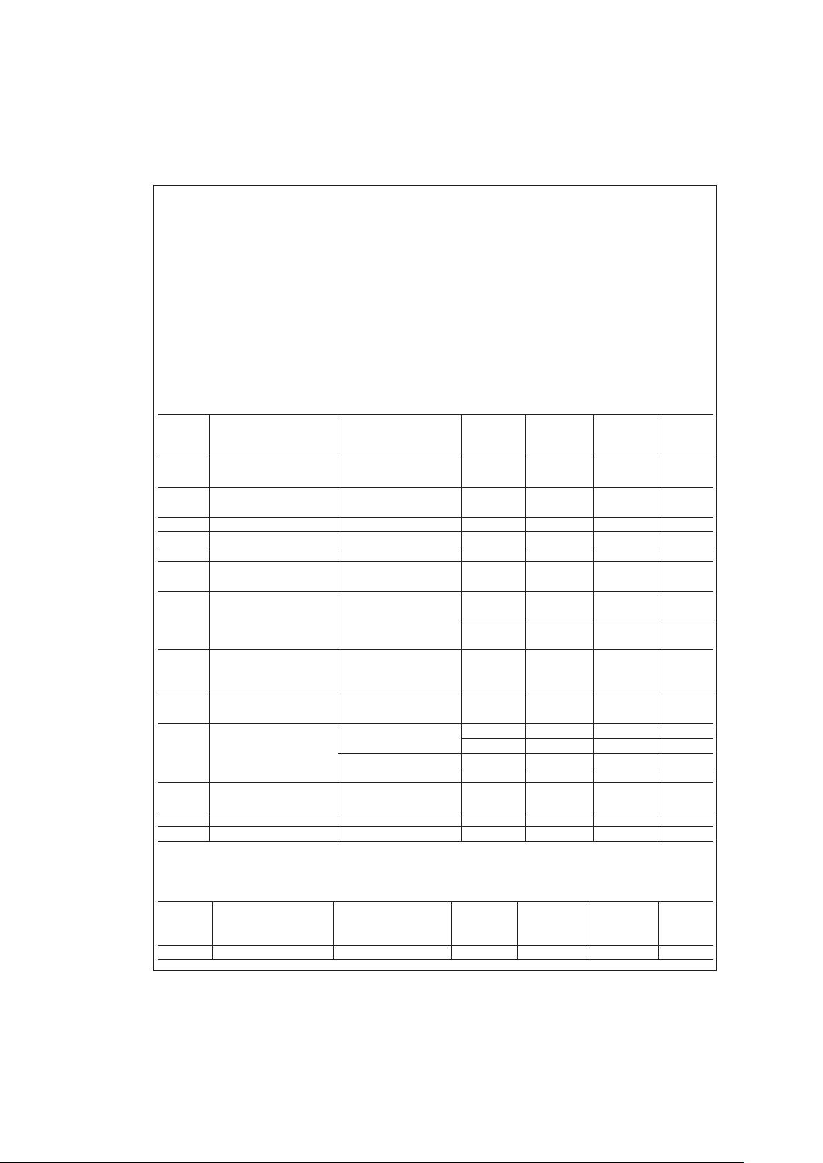
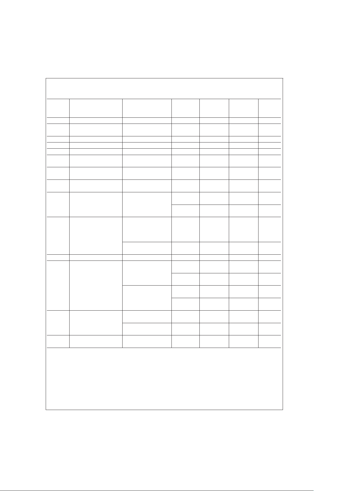
2.7V Electrical Characteristics
Unless otherwise specified, all limits guaranteed for T
J
=
25˚C, V
+
=
2.7V, V
−
=
0V, V
CM
=
V
O
=
V
+
/2 and R
L
>
1MΩ.Bold-
face limits apply at the temperature extremes.
Typ LMC7101AI LMC7101BI
Symbol Parameter Conditions (Note 5) Limit Limit Units
(Note 6) (Note 6)
V
OS
Input Offset Voltage V
+
=
2.7V 0.11 6 9 mV
max
TCV
OS
Input Offset Voltage 1 µV/˚C
Average Drift
I
B
Input Bias Current 1.0 64 64 pA max
I
OS
Input Offset Current 0.5 32 32 pA max
R
IN
Input Resistance
>
1 Tera Ω
CMRR Common-Mode 0V ≤ V
CM
≤ 2.7V 70 55 50 dB
Rejection Ratio V
+
=
2.7V min
V
CM
Input Common-Mode V
+
=
V 0.0 0.0 0.0 V
Voltage Range For CMRR ≥ 50 dB min
3.0 2.7 2.7 V
max
PSRR Power Supply V
+
=
1.35V to 1.65V dB
Rejection Ratio V
−
=
−1.35V to −1.65V 60 50 45 min
V
CM
=
0
C
IN
Common-Mode Input 3 pF
Capacitance
V
O
Output Swing R
L
=
2kΩ 2.45 2.15 2.15 V min
0.25 0.5 0.5 V max
R
L
=
10 kΩ 2.68 2.64 2.64 V min
0.025 0.06 0.06 V max
I
S
Supply Current 0.5 0.81 0.81 mA
0.95 0.95 max
SR Slew Rate (Note 8) 0.7 V/µs
GBW Gain-Bandwidth Product 0.6 MHz
3V DC Electrical Characteristics
Unless otherwise specified, all limits guaranteed for T
J
=
25˚C, V
+
=
3V, V
−
=
0V, V
CM
=
1.5V, V
O
=
V
+
/2 and R
L
=
1MΩ.
Boldface limits apply at the temperature extremes.
Typ LMC7101AI LMC7101BI
Symbol Parameter Conditions (Note 5) Limit Limit Units
(Note 6) (Note 6)
V
OS
Input Offset Voltage 0.11 4 7 mV
www.national.com 2
3V DC Electrical Characteristics (Continued)
Unless otherwise specified, all limits guaranteed for T
J
=
25˚C, V
+
=
3V, V
−
=
0V, V
CM
=
1.5V, V
O
=
V
+
/2 and R
L
=
1MΩ.
Boldface limits apply at the temperature extremes.
Typ LMC7101AI LMC7101BI
Symbol Parameter Conditions (Note 5) Limit Limit Units
(Note 6) (Note 6)
69max
TCV
OS
Input Offset Voltage 1 µV/˚C
Average Drift
I
B
Input Current 1.0 64 64 pA max
I
OS
Input Offset Current 0.5 32 32 pA max
R
IN
Input Resistance
>
1 Tera Ω
CMRR Common-Mode 0V ≤ V
CM
≤ 3V 74 64 60 db
Rejection Ratio V
+
=
3V min
V
CM
Input Common-Mode 0.0 0.0 0.0 V
Voltage Range For CMRR ≥ 50 dB min
3.3 3.0 3.0 V
max
PSRR Power Supply V
+
=
1.5V to 7.5V dB
Rejection Ratio V
−
=
−1.5V to −7.5V 80 68 60 min
V
O
=
V
CM
=
0
C
IN
Common-Mode Input 3 pF
Capacitance
V
O
Output Swing R
L
=
2kΩ 2.8 2.6 2.6 V min
0.2 0.4 0.4 V max
R
L
=
600Ω 2.7 2.5 2.5 V min
0.37 0.6 0.6 V max
I
S
Supply Current 0.5 0.81 0.81 mA
0.95 0.95 max
www.national.com3
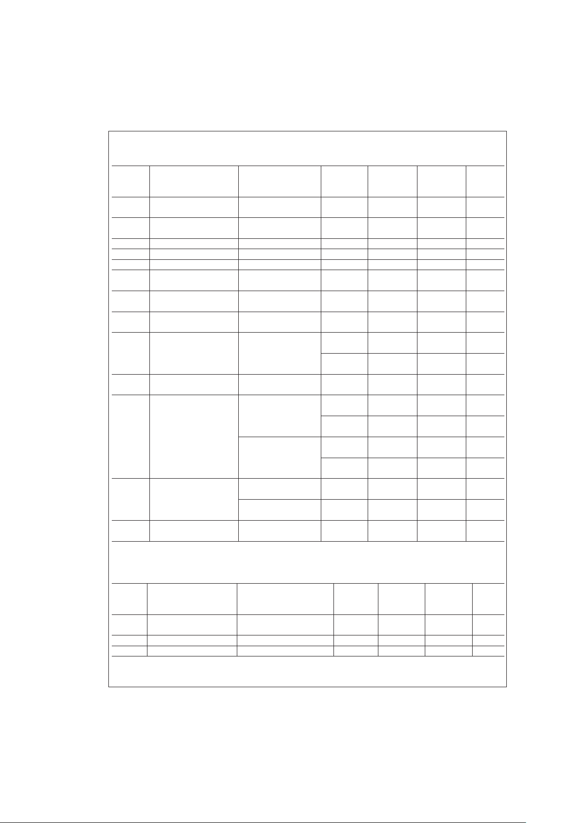
5V DC Electrical Characteristics
Unless otherwise specified, all limits guaranteed for T
J
=
25˚C, V
+
=
5V, V
−
=
0V, V
CM
=
1.5V, V
O
=
V
+
/2 and R
L
=
1MΩ.
Boldface limits apply at the temperature extremes.
Typ LMC7101AI LMC7101BI
Symbol Parameter Conditions (Note 5) Limit Limit Units
(Note 6) (Note 6)
V
OS
Input Offset Voltage V
+
=
5V 0.11 3 7 mV
59max
TCV
OS
Input Offset Voltage 1.0 µV/˚C
Average Drift
I
B
Input Current 1 64 64 pA max
I
OS
Input Offset Current 0.5 32 32 pA max
R
IN
Input Resistance
>
1 Tera Ω
CMRR Common-Mode 0V ≤ V
CM
≤ 5V 82 65 60 db
Rejection Ratio 60 55 min
+PSRR Positive Power Supply V
+
=
5V to 15V 82 70 65 dB
Rejection Ratio V
−
=
0V, V
O
=
1.5V 65 62 min
−PSRR Negative Power Supply V
−
=
−5V to −15V 82 70 65 dB
Rejection Ratio V
+
=
0V, V
O
=
−1.5V 65 62 min
V
CM
Input Common-Mode For CMRR ≥ 50 dB −0.3 −0.20 −0.20 V
Voltage Range 0.00 0.00 min
5.3 5.20 5.20 V
5.00 5.00 max
C
IN
Common-Mode 3 pF
Input Capacitance
V
O
Output Swing R
L
=
2kΩ 4.9 4.7 4.7 V
4.6 4.6 min
0.1 0.18 0.18 V
0.24 0.24 max
R
L
=
600Ω 4.7 4.5 4.5 V
4.24 4.24 min
0.3 0.5 0.5 V
0.65 0.65 max
I
SC
Output Short Circuit Sourcing, V
O
=
0V 24 16 16 mA
Current 11 11 min
Sinking, V
O
=
5V 19 11 11 mA
7.5 7.5 min
I
S
Supply Current 0.5 0.85 0.85 mA
1.0 1.0 max
5V AC Electrical Characteristics
Unless otherwise specified, all limits guaranteed for T
J
=
25˚C, V
+
=
5V, V
−
=
0V, V
CM
=
1.5V, V
O
=
V
+
/2 and R
L
=
1MΩ.
Boldface limits apply at the temperature extremes.
Typ LMC7101AI LMC7101BI
Symbol Parameter Conditions (Note 5) Limit Limit Units
(Note 6) (Note 6)
T.H.D. Total Harmonic F=10 kHz, A
V
=
−2 0.01
%
Distortion R
L
=
10 kΩ,V
O
=
4.0 V
PP
SR Slew Rate 1.0 V/µs
GBW Gain__Bandwidth Product 1.0 MHz
www.national.com 4
15V DC Electrical Characteristics
Unless otherwise specified, all limits guaranteed for T
J
=
25˚C, V
+
=
15V, V
−
=
0V, V
CM
=
1.5V, V
O
=
V
+
/2 and R
L
=
1MΩ.
Boldface limits apply at the temperature extremes.
Typ LMC7101AI LMC7101BI
Symbol Parameter Conditions (Note 5) Limit Limit Units
(Note 6) (Note 6)
V
OS
Input Offset Voltage 0.11 mV max
TCV
OS
Input Offset Voltage 1.0 µV/˚C
Average Drift
I
B
Input Current 1.0 64 64 pA max
I
OS
Input Offset Current 0.5 32 32 pA max
R
IN
Input Resistance
>
1 Tera Ω
CMRR Common-Mode 0V ≤ V
CM
≤ 15V 82 70 65 dB
Rejection Ratio 65 60 min
+PSRR Positive Power Supply V
+
=
5V to 15V 82 70 65 dB
Rejection Ratio V
−
=
0V, V
O
=
1.5V 65 62 min
−PSRR Negative Power Supply V
−
=
−5V to −15V 82 70 65 dB
Rejection Ratio V
+
=
0V, V
O
=
−1.5V 65 62 min
V
CM
Input Common-Mode V
+
=
5V −0.3 −0.20 −0.20 V
Voltage Range For CMRR ≥ 50 dB 0.00 0.00 min
15.3 15.20 15.20 V
15.00 15.00 max
A
V
Large Signal R
L
=
2kΩ Sourcing 340 80 80 V/mV
Voltage Gain (Note 7) 40 40
Sinking 24 15 15
10 10
R
L
=
600Ω Sourcing 300 34 34 V/mV
(Note 7) Sinking 15 6 6
C
IN
Input Capacitance 3 pF
V
O
Output Swing V
+
=
15V 14.7 14.4 14.4 V
R
L
=
2kΩ 14.2 14.2 min
0.16 0.32 0.32 V
0.45 0.45 max
V
+
=
15V 14.1 13.4 13.4 V
R
L
=
600Ω 13.0 13.0 min
0.5 1.0 1.0 V
1.3 1.3 max
I
SC
Output Short Circuit Sourcing, V
O
=
0V 50 30 30 mA
Current (Note 9) 20 20 min
Sinking, V
O
=
12V 50 30 30 mA
(Note 9) 20 20 min
I
S
Supply Current 0.8 1.50 1.50 mA
1.71 1.71 max
www.national.com5
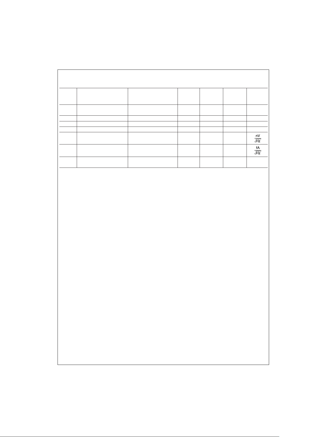
15V AC Electrical Characteristics
Unless otherwise specified, all limits guaranteed for T
J
=
25˚C, V
+
=
15V, V
−
=
0V, V
CM
=
1.5V, V
O
=
V
+
/2 and R
L
=
1MΩ.
Boldface limits apply at the temperature extremes.
Typ LMC7101AI LMC7101BI
Symbol Parameter Conditions (Note 5) Limit Limit Units
(Note 6) (Note 6)
SR Slew Rate V
+
=
15V 1.1 0.5 0.5 V/µs
(Note 8) 0.4 0.4 min
GBW Gain-Bandwidth Product V
+
=
15V 1.1 MHz
φ
m
Phase Margin 45 Deg
G
m
Gain Margin 10 dB
e
n
Input-Referred F=1 kHz
37
Voltage Noise V
CM
=
1V
i
n
Input-Referred F=1 kHz
1.5
Current Noise
T.H.D. Total Harmonic Distortion F=10 kHz, A
V
=
−2 0.01
%
R
L
=
10 kΩ,V
O
=
8.5 V
PP
Note 1: Absolute Maximum Ratings indicate limits beyond which damage to the device may occur. Operating Ratings indicate conditions for which the device is intended to be functional, but specific performance is not guaranteed. For guaranteed specifications and the test conditions, see the Electrical Characteristics.
Note 2: Human body model, 1.5 kΩ in series with 100 pF.
Note 3: Applies to both single-supply and split-supply operation. Continuous short operation at elevated ambient temperature can result in exceeding the maximum
allowed junction temperature at 150˚C.
Note 4: The maximum power dissipation is a function of T
J(max)
, θJAand TA. The maximum allowable power dissipation at any ambient temperature is PD=(T
J(max)
−TA)/θJA. All numbers apply for packages soldered directly into a PC board.
Note 5: Typical Values represent the most likely parametric norm.
Note 6: All limits are guaranteed by testing or statistical analysis.
Note 7: V
+
=
15V, V
CM
=
1.5V and R
L
connect to 7.5V. For Sourcing tests, 7.5V ≤ VO≤ 12.5V. For Sinking tests, 2.5V ≤ VO≤ 7.5V.
Note 8: V
+
=
15V.Connected as a Voltage Follower with a 10V step input. Number specified is the slower of the positive and negative slew rates. R
L
=
100 kΩ con-
nected to 7.5V.Amp excited with 1 kHz to produce V
O
=
10 V
PP
.
Note 9: Do not short circuit output to V
+
when V+is greater than 12V or reliability will be adversely affected.
www.national.com 6
 Loading...