

NSC LMC6953CMX, LMC6953CM Datasheet
LMC6953
PCI Local Bus Power Supervisor
LMC6953 PCI Local Bus Power Supervisor
April 1998
General Description
The LMC6953 is a voltage supervisory chip designed to
meet PCI (Peripheral Component Interconnect) Specifications Revision 2.1. It monitors 5V and 3.3V power supplies.
In cases of power-up, power-down, brown-out, power failure
and manual reset interrupt, the LMC6953 provides an active
low reset. RESET holds low for 100 ms after both 5V and
3.3V powers recover, or after manual reset signal returns to
high state. The external capacitor on pin 8 adjusts the reset
delay.
This part is ideal on PCI motherboards or add-in cards toensure the integrity of the entire system when there is a fault
condition. The activelowresetsetsthe microprocessor or local device in a known state.
The LMC6953 has a built-in bandgap reference that accurately determines all the threshold voltages. The internal reset delay circuitry eliminates additional discrete components.
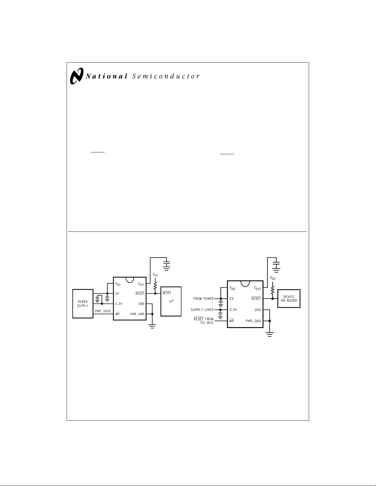
Typical Application Circuits
On Mother Board
Features
n Compliant to PCI specifications revision 2.1.
n Under and over voltage detectors for 5V and 3.3V
n Power failure detection (5V falling under 3.3V by
300 mV max)
n Manual reset input pin
n Guaranteed RESET assertion at V
n Integrated reset delay circuitry
n Open drain output
n Adjustable reset delay
n Response time for over and under voltage detection:
490 ns Max
n Power failure response time: 90 ns Max
n Requires minimal external components
=
1.5V
DD
Applications
n Desktop PCs
n PCI-Based Systems
n Network servers
On Add-in Cards
DS012846-23
DS012846-24
© 1998 National Semiconductor Corporation DS012846 www.national.com
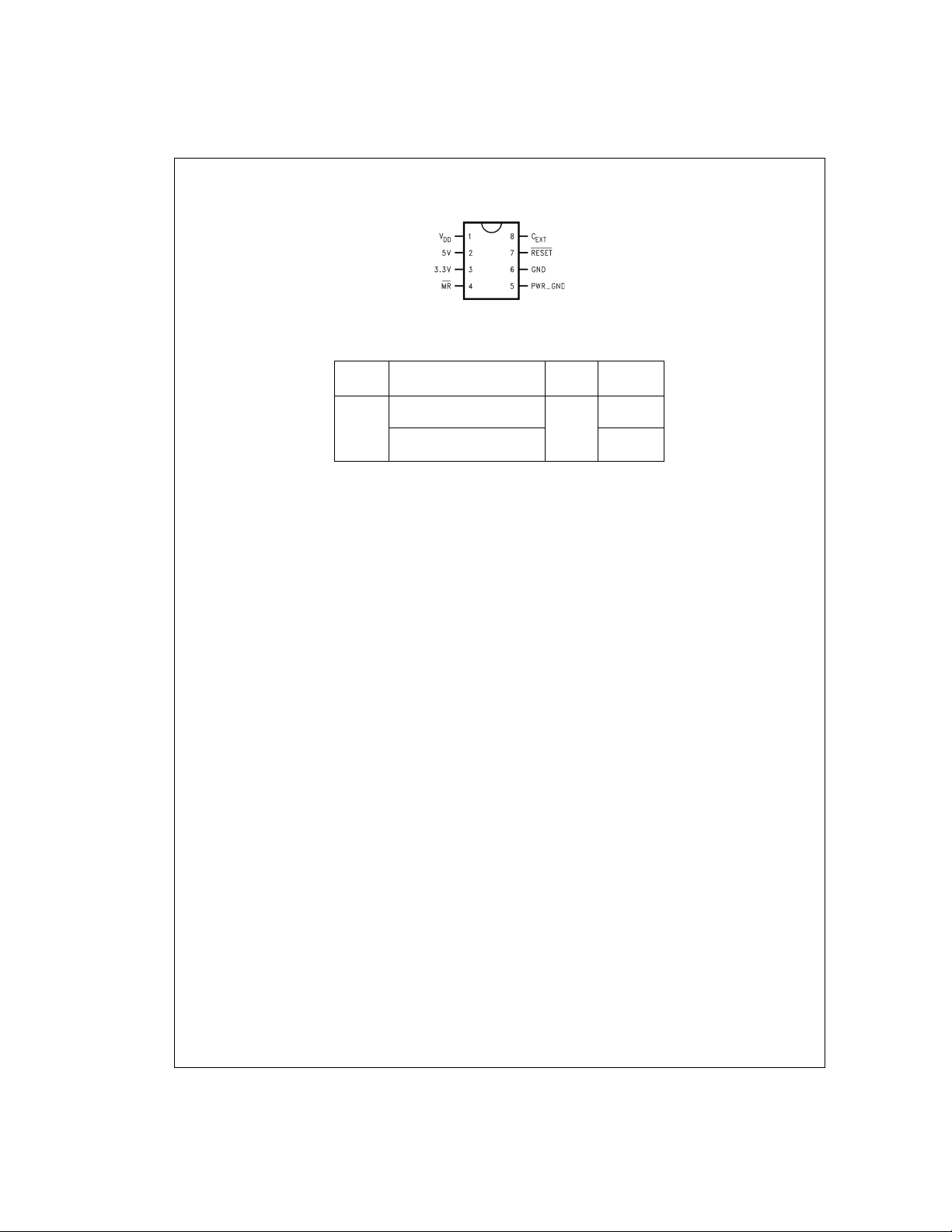
Connection Diagram
Ordering Information
Package Industrial Temp Range NSC Supplied
8-Pin
Small
Outline LMC6953CMX 2.5k Tape
8–Pin SO
DS012846-2
Top View
−40˚C to +85˚C Drawing As
LMC6953CM M08A Rails
and Reel
www.national.com 2
Absolute Maximum Ratings (Note 1)
If Military/Aerospace specified devices are required,
please contact the National Semiconductor Sales Office/
Distributors for availability and specifications.
ESD Tolerance (Note 2)
Human Body Model 2 kV
Machine Model 200V
Voltage at Input Pin 7V
Supply Voltage 7V
Current at Output Pin 15 mA
Current at Power Supply Pin (Note 3) 10 mA
Lead Temp. (Soldering, 10 sec.) 260˚C
Storage Temperature Range −65˚C to +150˚C
Junction Temperature 150˚C
Operating Ratings (Note 1)
Supply Voltage 1.5V to 6V
Junction Temperature Range
LMC6953C −40˚C to +85˚C
Thermal Resistance (θ
M Package 165˚C/W
)
JA
DC Electrical Characteristics
Unless otherwise specified, all boldface limits guaranteed for T
0.01 µF. Typical numbers are room temperature (25˚C) performance.
=
−40˚C to +85˚C, V
J
Symbol Parameter Conditions Min Typ Max Units
V
H5
V
L5
V
H3.3
V
L3.3
V
MR
V
PF
VDDOver-Voltage Threshold TJ= 0˚C to 70˚C
(Note 4)
T
= −40˚C to 85˚C
J
(Note 4)
VDDUnder-Voltage Threshold TJ= 0˚C to 70˚C
(Note 4)
= −40˚C to 85˚C
T
J
(Note 4)
3.3V Over-Voltage Threshold TJ= 0˚C to 70˚C
(Note 5)
= −40˚C to 85˚C
T
J
(Note 5)
3.3V Under-Voltage Threshold TJ= 0˚C to 70˚C
(Note 5)
= −40˚C to 85˚C
T
J
(Note 5)
Manual RESET Threshold 2.50 2.80 V
Power Failure Differential Voltage (Note 6) 150 300 mV
(3.3V Pin–5V Pin)
R
IN
V
OL
I
S
Input Resistance at 5V and 3.3V Pins 35 kΩ
RESET Output Low TJ= 0˚C to 70˚C
= 1.5V to 6V
V
DD
= −40˚C to 85˚C
T
J
= 1.55V to 6V
V
DD
Supply Current (Note 3) 0.8 1.50 mA
=
5V, R
DD
PULL-UP
=
4.7 kΩ and C
5.45 5.60 5.75 V
5.30 5.60 5.90 V
4.25 4.40 4.55 V
4.10 4.40 4.70 V
3.80 3.95 4.10 V
3.60 3.95 4.30 V
2.50 2.65 2.80 V
2.30 2.65 3.00 V
0.05 0.10 V
EXT
=
AC Electrical Characteristics
Unless otherwise specified, all boldface limits guaranteed for T
=
0.01 µF. Typical numbers are room temperature (25˚C) performance.
=
−40˚C to 85˚C, V
J
Symbol Parameter Conditions Typ LMC6953 Units
t
D
t
PF
t
RESET
Note 1: Absolute Maximum Ratings indicate limits beyond which damage to the device may occur. Operating Ratings indicate conditions for which the device is intended to be functional, but specific performance is not guaranteed. For guaranteed specifications and the test conditions, see the Electrical Characteristics.
Note 2: Human body model, 1.5 kΩ in series with 100 pF. Machine model. 200Ω in series with 100 pF.
Over or Under Voltage Response Time (Note 7) 150 490 ns
Power Failure Response Time (Note 8) 40 90 ns
Reset Delay C
=
0.01 µF 100 ms
EXT
3 www.national.com
=
5V, R
DD
PULL-UP
=
4.7 kΩ and C
EXT
Limit
max
max
AC Electrical Characteristics (Continued)
Note 3: Supply current measured at pins 1, 2, and 3. The 4.7 kΩ pull-up resistor on pin 7 is not tied to VDDin this measurement.
Note 4: PCI Specifications Revision 2.1, Section 4.2.1.1 and Section 4.3.2.
Note 5: PCI Specifications Revision 2.1, Section 4.2.2.1 and Section 4.3.2.
Note 6: PCI Specifications Revision 2.1 and Section 4.3.2.
Note 7: PCISpecifications Revision 2.1, Section 4.3.2. The response time is measured individually with
drive applied to pin 3 and taking the worst number of the four measurements.
Note 8: PCI Specifications Revision 2.1, Section 4.3.2. The power failure response time is measured with a signal changing from 5V to 3V applied to pin 2 and a
3.3V DC applied to pin 3.
±
750 mV of overdrive applied to pin 2 then±600 mV of over-
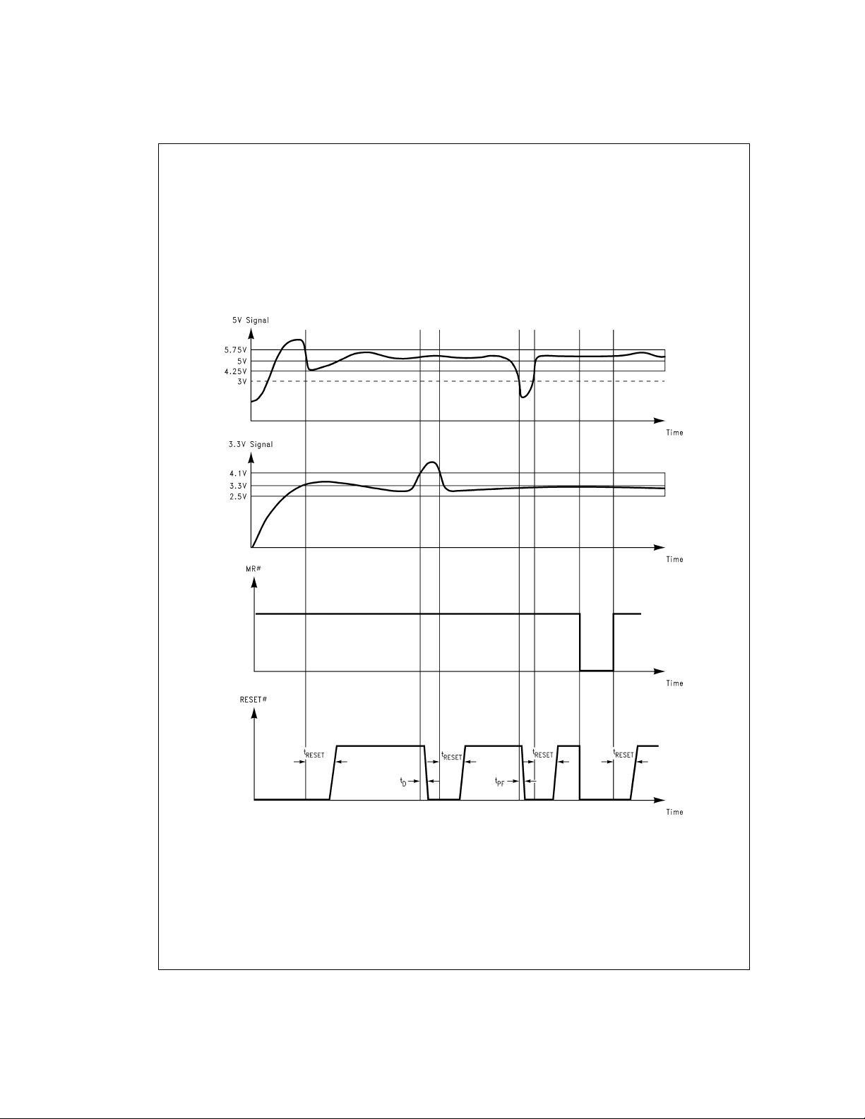
LMC6953 Timing Diagram
Note: t
www.national.com 4
and tPFare not to scale.
RESET,tD
DS012846-3
 Loading...