

NSC LMC6464BIN, LMC6464BIM, LMC6464AIN, LMC6464AIMX, LMC6464AIM Datasheet
...
LMC6462 Dual/LMC6464 Quad
Micropower, Rail-to-Rail Input and Output CMOS
Operational Amplifier
General Description
The LMC6462/4 is a micropower version of the popular
LMC6482/4, combining Rail-to-Rail Input and Output Range
with very low power consumption.
The LMC6462/4 provides an input common-mode voltage
range that exceeds both rails.The rail-to-rail output swing of
the amplifier, guaranteed for loads down to 25 kΩ, assures
maximum dynamic sigal range. This rail-to-rail performance
of the amplifier, combined with its high voltage gain makes it
unique among rail-to-rail amplifiers. The LMC6462/4 is an
excellent upgrade for circuits using limited common-mode
range amplifiers.
The LMC6462/4, with guaranteed specifications at 3V and
5V, is especially well-suited for low voltage applications. A
quiescent power consumption of 60 µW per amplifier (at V
S
=
3V) can extend the useful life of battery operated systems.
The amplifier’s 150 fA input current, low offset voltage of
0.25 mV, and 85 dB CMRR maintain accuracy in
battery-powered systems.
Features
(Typical unless otherwise noted)
n Ultra Low Supply Current 20 µA/Amplifier
n Guaranteed Characteristics at 3V and 5V
n Rail-to-Rail Input Common-Mode Voltage Range
n Rail-to-Rail Output Swing
(within 10 mV of rail, V
S
=
5V and R
L
=
25 kΩ)
n Low Input Current 150 fA
n Low Input Offset Voltage 0.25 mV
Applications
n Battery Operated Circuits
n Transducer Interface Circuits
n Portable Communication Devices
n Medical Applications
n Battery Monitoring
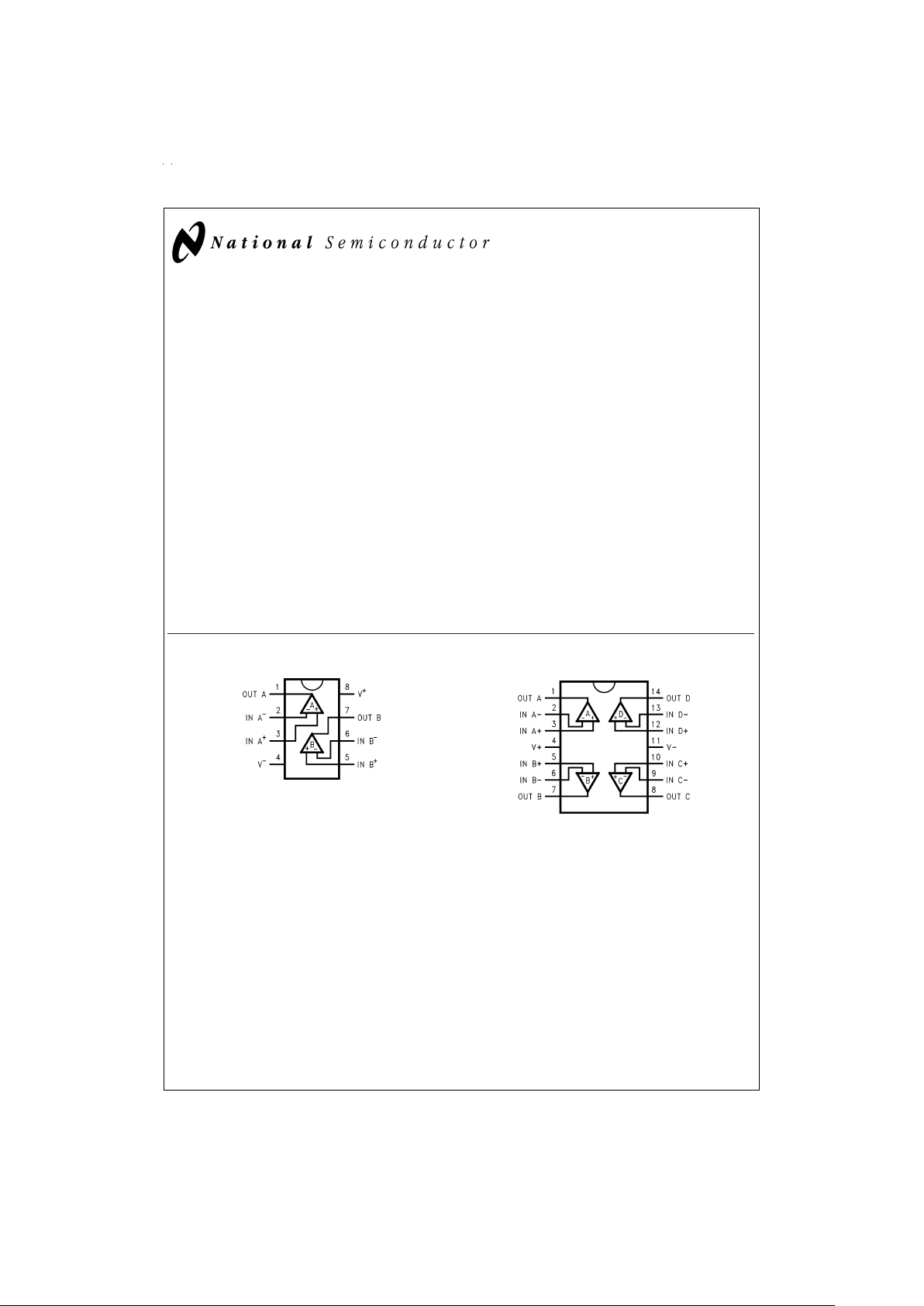
8-Pin DIP/SO
DS012051-1
Top View
14-Pin DIP/SO
DS012051-2
Top View
May 1999
LMC6462 Dual/LMC6464 Quad Micropower, Rail-to-Rail Input and Output CMOS Operational
Amplifier
© 1999 National Semiconductor Corporation DS012051 www.national.com
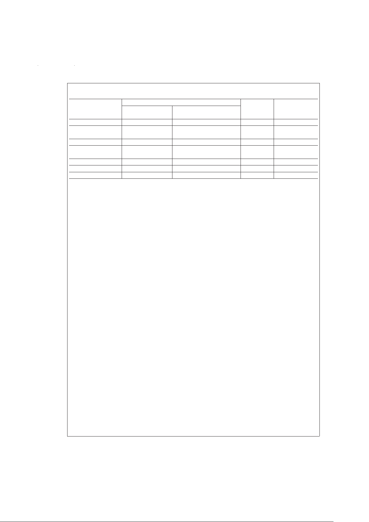
Ordering Information
Package Temperature Range NSC Transport
Military Industrial Drawing Media
−55˚C to +125˚C −40˚C to +85˚C
8-Pin Molded DIP LMC6462AMN LMC6462AIN, LMC6462BIN N08E Rails
8-Pin SO-8 LMC6462AIM, LMC6462BIM M08A Rails
LMC6462AIMX, LMC6462BIMX M08A Tape and Reel
14-Pin Molded DIP LMC6464AMN LMC6464AIN, LMC6464BIN N14A Rails
14-Pin SO-14 LMC6464AIM, LMC6464BIM M14A Rails
LMC6464AIMX, LMC6464BIMX M14A Tape and Reel
8-Pin Ceramic DIP LMC6462AMJ-QML J08A Rails
14-Pin Ceramic DIP LMC6464AMJ-QML J14A Rails
14-Pin Ceramic SOIC LMC6464AMWG-QML WG14A Trays
www.national.com 2
Absolute Maximum Ratings (Note 1)
If Military/Aerospace specified devices are required,
please contact the National Semiconductor Sales Office/
Distributors for availability and specifications.
ESD Tolerance (Note 2) 2.0 kV
Differential Input Voltage
±
Supply Voltage
Voltage at Input/Output Pin (V
+
) + 0.3V, (V−) − 0.3V
Supply Voltage (V
+−V−
) 16V
Current at Input Pin (Note 12)
±
5mA
Current at Output Pin
(Notes 3, 8)
±
30 mA
Current at Power Supply Pin 40 mA
Lead Temp. (Soldering, 10 sec.) 260˚C
Storage Temperature Range −65˚C to +150˚C
Junction Temperature (Note 4) 150˚C
Operating Ratings (Note 1)
Supply Voltage 3.0V ≤ V
+
≤ 15.5V
Junction Temperature Range
LMC6462AM, LMC6464AM −55˚C ≤ T
J
≤ +125˚C
LMC6462AI, LMC6464AI −40˚C ≤ T
J
≤ +85˚C
LMC6462BI, LMC6464BI −40˚C ≤ T
J
≤ +85˚C
Thermal Resistance (θ
JA
)
N Package, 8-Pin Molded DIP 115˚C/W
M Package, 8-Pin Surface Mount 193˚C/W
N Package, 14-Pin Molded DIP 81˚C/W
M Package, 14-Pin
Surface Mount 126˚C/W
5V DC Electrical Characteristics
Unless otherwise specified, all limits guaranteed for T
J
=
25˚C, V
+
=
5V, V
−
=
0V, V
CM
=
V
O
=
V
+
/2 and R
L
>
1M. Boldface
limits apply at the temperature extremes.
LMC6462AI LMC6462BI LMC6462AM
Symbol Parameter Conditions Typ LMC6464AI LMC6464BI LMC6464AM Units
(Note 5) Limit Limit Limit
(Note 6) (Note 6) (Note 6)
V
OS
Input Offset Voltage 0.25 0.5 3.0 0.5 mV
1.2 3.7 1.5 max
TCV
OS
Input Offset Voltage 1.5 µV/˚C
Average Drift
I
B
Input Current (Note 13) 0.15 10 10 200 pA max
I
OS
Input Offset Current (Note 13) 0.075 5 5 100 pA max
C
IN
Common-Mode 3 pF
Input Capacitance
R
IN
Input Resistance
>
10 Tera Ω
CMRR Common Mode 0V ≤ V
CM
≤ 15.0V, 85 70 65 70 dB
min
Rejection Ratio V
+
=
15V 67 62 65
0V ≤ V
CM
≤ 5.0V 85 70 65 70
V
+
=
5V 67 62 65
+PSRR Positive Power Supply 5V ≤ V
+
≤ 15V, 85 70 65 70 dB
Rejection Ratio V
−
=
0V, V
O
=
2.5V 67 62 65 min
−PSRR Negative Power Supply −5V ≤ V
−
≤ −15V, 85 70 65 70 dB
Rejection Ratio V
+
=
0V, V
O
=
−2.5V 67 62 65 min
V
CM
Input Common-Mode V
+
=
5V −0.2 −0.10 −0.10 −0.10 V
Voltage Range For CMRR ≥ 50 dB 0.00 0.00 0.00 max
5.30 5.25 5.25 5.25 V
5.00 5.00 5.00 min
V
+
=
15V −0.2 −0.15 −0.15 −0.15 V
For CMRR ≥ 50 dB 0.00 0.00 0.00 max
15.30 15.25 15.25 15.25 V
15.00 15.00 15.00 min
www.national.com3
5V DC Electrical Characteristics (Continued)
Unless otherwise specified, all limits guaranteed for T
J
=
25˚C, V
+
=
5V, V
−
=
0V, V
CM
=
V
O
=
V
+
/2 and R
L
>
1M. Boldface
limits apply at the temperature extremes.
LMC6462AI LMC6462BI LMC6462AM
Symbol Parameter Conditions Typ LMC6464AI LMC6464BI LMC6464AM Units
(Note 5) Limit Limit Limit
(Note 6) (Note 6) (Note 6)
A
V
Large Signal R
L
=
100 kΩ Sourcing 3000 V/mV
Voltage Gain (Note 7) min
Sinking 400 V/mV
min
R
L
=
25 kΩ Sourcing 2500 V/mV
(Note 7) min
Sinking 200 V/mV
min
V
O
Output Swing V
+
=
5V 4.995 4.990 4.950 4.990 V
R
L
=
100 kΩ to V
+
/2 4.980 4.925 4.970 min
0.005 0.010 0.050 0.010 V
0.020 0.075 0.030 max
V
+
=
5V 4.990 4.975 4.950 4.975 V
R
L
=
25 kΩ to V
+
/2 4.965 4.850 4.955 min
0.010 0.020 0.050 0.020 V
0.035 0.150 0.045 max
V
+
=
15V 14.990 14.975 14.950 14.975 V
R
L
=
100 kΩ to V
+
/2 14.965 14.925 14.955 min
0.010 0.025 0.050 0.025 V
0.035 0.075 0.050 max
V
+
=
15V 14.965 14.900 14.850 14.900 V
R
L
=
25 kΩ to V
+
/2 14.850 14.800 14.800 min
0.025 0.050 0.100 0.050 V
0.150 0.200 0.200 max
I
SC
Output Short Circuit Sourcing, V
O
=
0V 27 19 19 19 mA
Current 15 15 15 min
V+=5V Sinking, V
O
=
5V 27 22 22 22 mA
17 17 17 min
I
SC
Output Short Circuit Sourcing, V
O
=
0V 38 24 24 24 mA
Current 17 17 17 min
V
+
=
15V Sinking, V
O
=
12V 75 55 55 55 mA
(Note 8) 45 45 45 min
I
S
Supply Current Dual, LMC6462 40 55 55 55 µA
V
+
=
+5V, V
O
=
V
+
/2 70 70 75 max
Quad, LMC6464 80 110 110 110 µA
V
+
=
+5V, V
O
=
V
+
/2 140 140 150 max
Dual, LMC6462 50 60 60 60 µA
V
+
=
+15V, V
O
=
V
+
/2 70 70 75 max
Quad, LMC6464 90 120 120 120 µA
V
+
=
+15V, V
O
=
V
+
/2 140 140 150 max
www.national.com 4
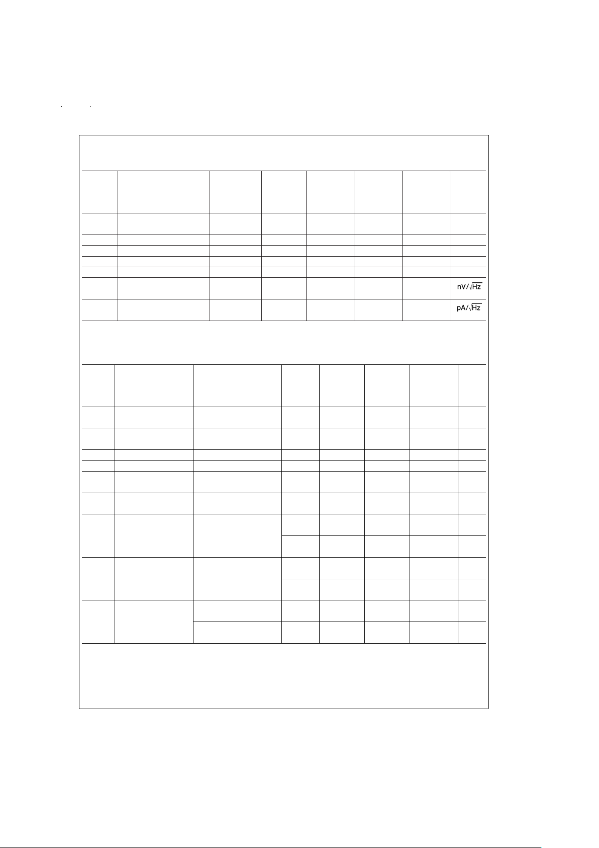
5V AC Electrical Characteristics
Unless otherwise specified, all limits guaranteed for T
J
=
25˚C, V
+
=
5V, V
−
=
0V, V
CM
=
V
O
=
V
+
/2 and R
L
>
1M. Boldface
limits apply at the temperature extremes.
LMC6462AI LMC6462BI LMC6462AM
Symbol Parameter Conditions Typ LMC6464AI LMC6464BI LMC6464AM Units
(Note 5) Limit Limit Limit
(Note 6) (Note 6) (Note 6)
SR Slew Rate (Note 9) 28 15 15 15 V/ms
888min
GBW Gain-Bandwidth Product V
+
=
15V 50 kHz
φ
m
Phase Margin 50 Deg
G
m
Gain Margin 15 dB
Amp-to-Amp Isolation (Note 10) 130 dB
e
n
Input-Referred f=1 kHz 80
Voltage Noise V
CM
=
1V
i
n
Input-Referred f=1 kHz 0.03
Current Noise
3V DC Electrical Characteristics
Unless otherwise specified, all limits guaranteed for T
J
=
25˚C, V
+
=
3V, V
−
=
0V, V
CM
=
V
O
=
V
+
/2 and R
L
>
1M. Boldface
limits apply at the temperature extremes.
LMC6462AI LMC6462BI LMC6462AM
Symbol Parameter Conditions Typ LMC6464AI LMC6464BI LMC6464AM Units
(Note 5) Limit Limit Limit
(Note 6) (Note 6) (Note 6)
V
OS
Input Offset Voltage 0.9 2.0 3.0 2.0 mV
2.7 3.7 3.0 max
TCV
OS
Input Offset Voltage 2.0 µV/˚C
Average Drift
I
B
Input Current (Note 13) 0.15 10 10 200 pA
I
OS
Input Offset Current (Note 13) 0.075 5 5 100 pA
CMRR Common Mode 0V ≤ V
CM
≤ 3V 74 60 60 60 dB
Rejection Ratio min
PSRR Power Supply 3V ≤ V
+
≤ 15V, V
−
=
0V 80 60 60 60 dB
Rejection Ratio min
V
CM
Input Common-Mode For CMRR ≥ 50 dB −0.10 0.0 0.0 0.0 V
Voltage Range max
3.0 3.0 3.0 3.0 V
min
V
O
Output Swing R
L
=
25 kΩ to V
+
/2 2.95 2.9 2.9 2.9 V
min
0.15 0.1 0.1 0.1 V
max
I
S
Supply Current Dual, LMC6462 40 55 55 55 µA
V
O
=
V
+
/2 70 70 70
Quad, LMC6464 80 110 110 110 µA
V
O
=
V
+
/2 140 140 140 max
www.national.com5
3V AC Electrical Characteristics
Unless otherwise specified, V
+
=
3V, V
−
=
0V, V
CM
=
V
O
=
V
+
/2 and R
L
>
1M. Boldface limits apply at the temperature ex-
tremes.
LMC6462AI LMC6462BI LMC6462AM
Symbol Parameter Conditions Typ LMC6464AI LMC6464BI LMC6464AM Units
(Note 5) Limit Limit Limit
(Note 6) (Note 6) (Note 6)
SR Slew Rate (Note 11) 23 V/ms
GBW Gain-Bandwidth Product 50 kHz
Note 1: Absolute Maximum Ratings indicate limits beyond which damage to the device may occur. Operating Ratings indicate conditions for which the device is intended to be functional, but specific performance is not guaranteed. For guaranteed specifications and the test conditions, see the Electrical Characteristics.
Note 2: Human body model, 1.5 kΩ in series with 100 pF. All pins rated per method 3015.6 of MIL-STD-883. This is a class 2 device rating.
Note 3: Applies to both single supply and split-supply operation. Continuous short circuit operationatelevatedambienttemperaturecanresultinexceedingthe maxi-
mum allowed junction temperature of 150˚C. Output currents in excess of
±
30 mA over long term may adversely affect reliability.
Note 4: The maximum power dissipation is a function of T
J(max)
, θJA, and TA. The maximum allowable power dissipation at any ambient temperature is P
D
=
(T
J(max)
−TA)/θJA. All numbers apply for packages soldered directly into a PC board.
Note 5: Typical Values represent the most likely parametric norm.
Note 6: All limits are guaranteed by testing or statistical analysis.
Note 7: V
+
=
15V, V
CM
=
7.5V and R
L
connected to 7.5V. For Sourcing tests, 7.5V ≤ VO≤ 11.5V. For Sinking tests, 3.5V ≤ VO≤ 7.5V.
Note 8: Do not short circuit output to V
+
, when V+is greater than 13V or reliability will be adversely affected.
Note 9: V
+
=
15V. Connected as Voltage Follower with 10V step input. Number specified is the slower of either the positive or negative slew rates.
Note 10: Input referred, V
+
=
15V and R
L
=
100 kΩ connected to 7.5V. Each amp excited in turn with 1 kHz to produce V
O
=
12 V
PP
.
Note 11: Connected as Voltage Follower with 2V step input. Number specified is the slower of either the positive or negative slew rates.
Note 12: Limiting input pin current is only necessary for input voltages that exceed absolute maximum input voltage ratings.
Note 13: Guaranteed limits are dictated by tester limitations and not device performance. Actual performance is reflected in the typical value.
Note 14: For guaranteed Military Temperature Range parameters see RETSMC6462/4X.
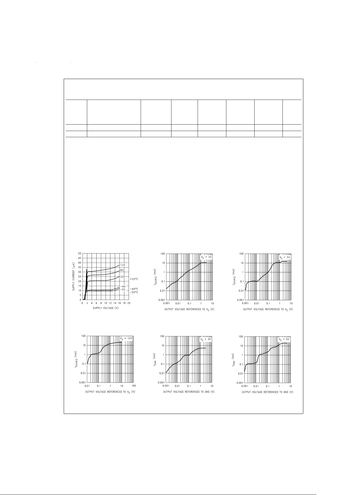
Typical Performance Characteristics V
S
=
+5V, Single Supply, T
A
=
25˚C unless otherwise specified
Supply Current vs
Supply Voltage
DS012051-30
Sourcing Current vs
Output Voltage
DS012051-31
Sourcing Current vs
Output Voltage
DS012051-32
Sourcing Current vs
Output Voltage
DS012051-33
Sinking Current vs
Output Voltage
DS012051-34
Sinking Current vs
Output Voltage
DS012051-35
www.national.com 6
 Loading...