

NSC LM2902N, LM2902MX, LM2902M, LM224J Datasheet
LM124/LM224/LM324/LM2902
Low Power Quad Operational Amplifiers
LM124/LM224/LM324/LM2902 Low Power Quad Operational Amplifiers
March 2000
General Description
The LM124 series consists of four independent, high gain,
internally frequency compensated operational amplifiers
which were designed specifically to operate from a single
power supply over a wide range of voltages. Operation from
split power supplies is also possible and the low power supply current drain is independent of the magnitude of the
power supply voltage.
Application areas include transducer amplifiers, DC gain
blocks and all the conventional op amp circuits which now
can be more easily implementedin single power supply systems. For example, the LM124 series can be directly operated off of the standard +5V power supply voltage which is
used in digital systems and will easily provide the required
interface electronics without requiring the additional
power supplies.
±
15V
Unique Characteristics
n In the linear mode the input common-mode voltage
range includes ground and the output voltage can also
swing to ground, even though operated from only a
single power supply voltage
n The unity gain cross frequency is temperature
compensated
n The input bias current is also temperature compensated
Advantages
n Eliminates need for dual supplies
n Four internally compensated op amps in a single
package
n Allows directly sensing near GND and V
to GND
n Compatible with all forms of logic
n Power drain suitable for battery operation
OUT
also goes
Features
n Internally frequency compensated for unity gain
n Large DC voltage gain 100 dB
n Wide bandwidth (unity gain) 1 MHz
(temperature compensated)
n Wide power supply range:
Single supply 3V to 32V
or dual supplies
n Very low supply current drain (700 µA)—essentially
independent of supply voltage
n Low input biasing current 45 nA
(temperature compensated)
n Low input offset voltage 2 mV
and offset current: 5 nA
n Input common-mode voltage range includes ground
n Differential input voltage range equal to the power
supply voltage
n Large output voltage swing 0V to V
±
1.5V to±16V
+
− 1.5V
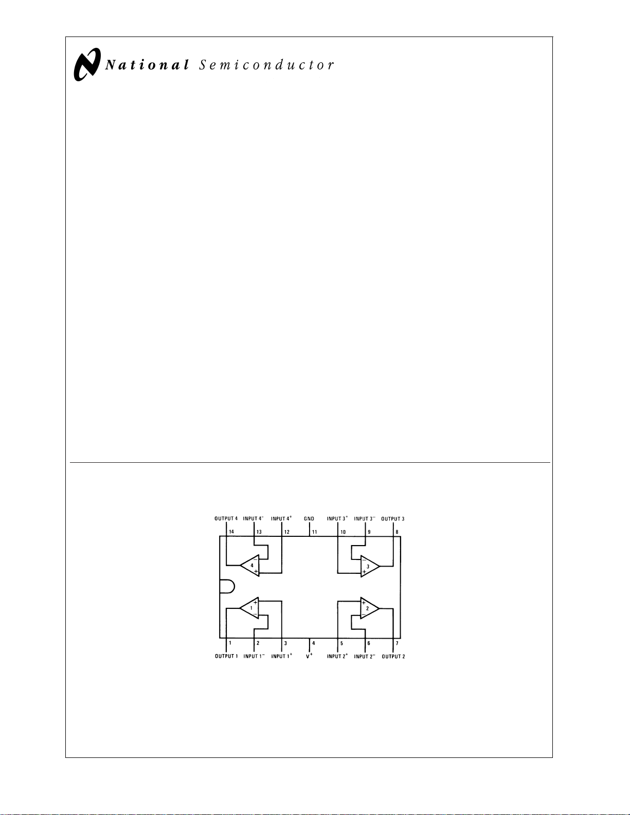
Connection Diagram
Dual-In-Line Package
DS009299-1
Top View
Order Number LM124J, LM124AJ, LM124J/883 (Note 2), LM124AJ/883 (Note 1), LM224J,
LM224AJ, LM324J, LM324M, LM324AM, LM2902M, LM324N, LM324AN, LM324MT, LM324MTX or LM2902N
LM124AJRQML and LM124AJRQMLV(Note 3)
See NS Package Number J14A, M14A or N14A
Note 1: LM124A available per JM38510/11006
Note 2: LM124 available per JM38510/11005
© 2000 National Semiconductor Corporation DS009299 www.national.com
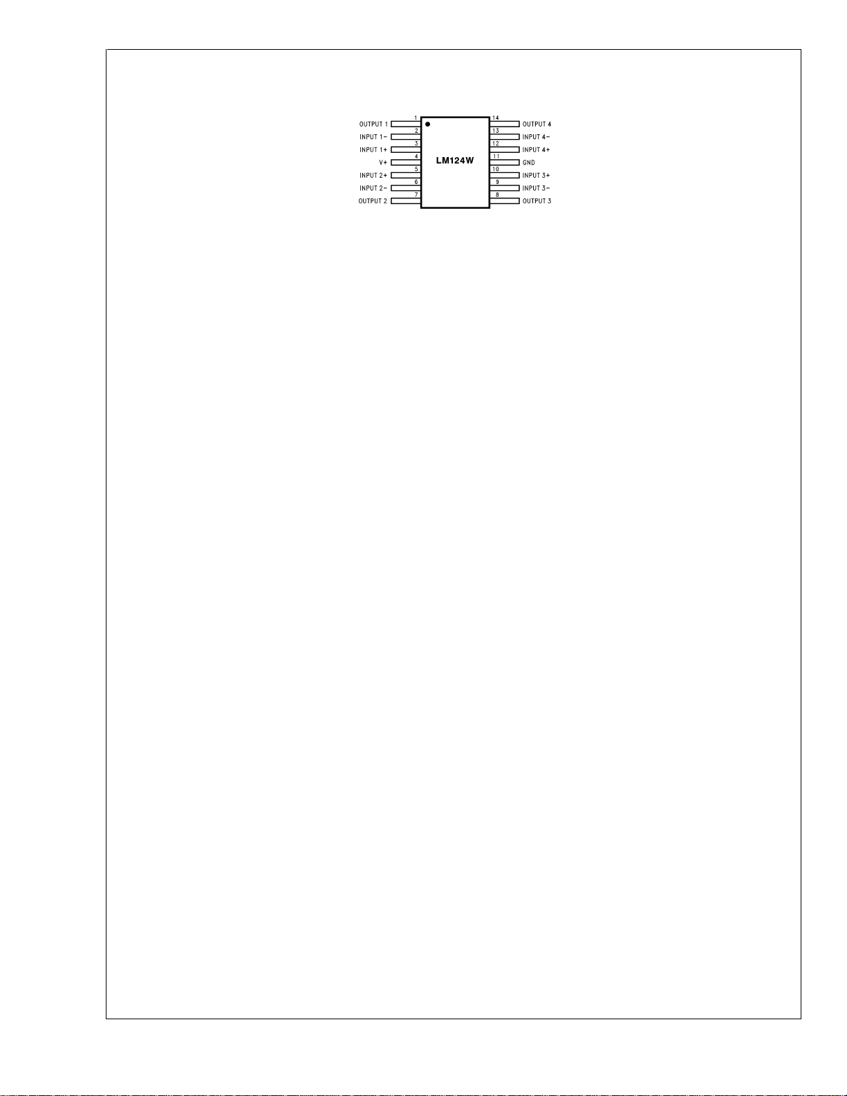
Connection Diagram (Continued)
Note 3: See STD Mil DWG 5962R99504 for Radiation Tolerant Device
LM124/LM224/LM324/LM2902
Order Number LM124AW/883 or LM124W/883
LM124AWRQML and LM124AWRQMLV(Note 3)
LM124AWGRQML and LM124AWGRQMLV(Note 3)
DS009299-33
See NS Package Number W14B
See NS Package Number WG14A
www.national.com 2
Absolute Maximum Ratings (Note 12)
If Military/Aerospace specified devices are required,
please contact the National Semiconductor Sales Office/
Distributors for availability and specifications.
LM124/LM224/LM324 LM2902
Supply Voltage, V
+
Differential Input Voltage 32V 26V
Input Voltage −0.3V to +32V −0.3V to +26V
Input Current
<
(V
−0.3V) (Note 6) 50 mA 50 mA
IN
Power Dissipation (Note 4)
Molded DIP 1130 mW 1130 mW
Cavity DIP 1260 mW 1260 mW
Small Outline Package 800 mW 800 mW
Output Short-Circuit to GND
(One Amplifier) (Note 5)
+
V
≤ 15V and TA= 25˚C Continuous Continuous
Operating Temperature Range −40˚C to +85˚C
LM324/LM324A 0˚C to +70˚C
LM224/LM224A −25˚C to +85˚C
LM124/LM124A −55˚C to +125˚C
Storage Temperature Range −65˚C to +150˚C −65˚C to +150˚C
Lead Temperature (Soldering, 10 seconds) 260˚C 260˚C
Soldering Information
Dual-In-Line Package
Soldering (10 seconds) 260˚C 260˚C
Small Outline Package
Vapor Phase (60 seconds) 215˚C 215˚C
Infrared (15 seconds) 220˚C 220˚C
See AN-450 “Surface Mounting Methods and Their Effect on Product Reliability” for other methods of soldering surface mount
devices.
ESD Tolerance (Note 13) 250V 250V
LM124A/LM224A/LM324A
32V 26V
LM124/LM224/LM324/LM2902
Electrical Characteristics
V+= +5.0V, (Note 7), unless otherwise stated
Parameter Conditions
Input Offset Voltage (Note 8) T
Input Bias Current I
(Note 9) T
Input Offset Current I
Input Common-Mode V
Voltage Range (Note 10) T
Supply Current Over Full Temperature Range
Large Signal V
Voltage Gain (V
Common-Mode DC, V
Rejection Ratio T
IN(+)
IN(+)
T
R
V
V
A
A
+
A
L
+
+
+
O
A
= 25˚C 1 2 1 3 2 3 mV
A
or I
IN(−),VCM
= 25˚C
or I
IN(−),VCM
= 25˚C
= 30V, (LM2902, V+= 26V), 0 V+−1.5 0 V+−1.5 0 V+−1.5 V
= 25˚C
=∞On All Op Amps mA
= 30V (LM2902 V+= 26V) 1.5 3 1.5 3 1.5 3
= 5V 0.7 1.2 0.7 1.2 0.7 1.2
= 15V, RL≥ 2kΩ, 50 100 50 100 25 100 V/mV
= 1V to 11V), TA= 25˚C
CM
= 25˚C
= 0V,
= 0V, 2 10 2 15 5 30 nA
=0VtoV+− 1.5V, 70 85 70 85 65 85 dB
LM124A LM224A LM324A
Min Typ Max Min Typ Max Min Typ Max
20 50 40 80 45 100 nA
www.national.com3
Units
Electrical Characteristics (Continued)
V+= +5.0V, (Note 7), unless otherwise stated
Parameter Conditions
Power Supply V
Rejection Ratio (LM2902, V
Amplifier-to-Amplifier f = 1 kHz to 20 kHz, T
+
=5Vto30V
T
= 25˚C
A
+
= 5V to 26V), 65 100 65 100 65 100 dB
= 25˚C −120 −120 −120 dB
A
Coupling (Note 11) (Input Referred)
+
Output Current Source V
LM124/LM224/LM324/LM2902
Sink V
= 1V, V
IN
+
= 15V, VO= 2V, TA= 25˚C mA
V
−
= 1V, V
IN
+
V
= 15V, VO= 2V, TA= 25˚C
−
= 1V, V
V
IN
+
= 15V, VO= 200 mV, TA= 25˚C
V
Short Circuit to Ground (Note 5) V
−
= 0V, 20 40 20 40 20 40
IN
+
= 0V, 10 20 10 20 10 20
IN
+
= 0V, 12 50 12 50 12 50 µA
IN
+
= 15V, TA= 25˚C 40 60 40 60 40 60 mA
Input Offset Voltage (Note 8) 4 4 5 mV
Input Offset R
=0Ω 7 20 7 20 7 30 µV/˚C
S
Voltage Drift
Input Offset Current I
Input Offset R
IN(+)−IIN(−),VCM
=0Ω 10 200 10 200 10 300 pA/˚C
S
=0V 303075nA
Current Drift
Input Bias Current I
Input Common-Mode V
Voltage Range (Note 10) (LM2902, V
Large Signal V
Voltage Gain (V
Output Voltage V
OH
Swing (LM2902, V
V
OL
Output Current Source V
Sink V
or I
IN(+)
IN(−)
+
= +30V 0 V+−2 0 V+−2 0 V+−2 V
+
+
= +15V
Swing = 1V to 11V) 25 25 15 V/mV
O
R
≥ 2kΩ
L
= 26V)
V+= 30V RL=2kΩ 26 26 26 V
+
= 26V) RL=10kΩ 27 28 27 28 27 28
V+= 5V, RL=10kΩ 520 520 520mV
=2V V
O
+
= +1V, 10 20 10 20 10 20
IN
−
= 0V,
V
IN
V+= 15V
−
= +1V, 10 15 5 8 5 8
IN
+
= 0V,
V
IN
V+= 15V
LM124A LM224A LM324A
Min Typ Max Min Typ Max Min Typ Max
40 100 40 100 40 200 nA
Units
mA
Electrical Characteristics
V+= +5.0V, (Note 7), unless otherwise stated
Parameter Conditions
Input Offset Voltage (Note 8) T
Input Bias Current I
(Note 9) T
Input Offset Current I
Input Common-Mode V
Voltage Range (Note 10) T
IN(+)
IN(+)
T
A
A
+
A
Supply Current Over Full Temperature Range
R
L
+
V
+
V
Large Signal V
Voltage Gain (V
+
O
www.national.com 4
= 25˚C 2 5 2 7 2 7 mV
A
or I
IN(−),VCM
= 0V,
= 25˚C
or I
IN(−),VCM
= 0V, 3 30 5 50 5 50 nA
= 25˚C
= 30V, (LM2902, V+= 26V), 0 V+−1.5 0 V+−1.5 0 V+−1.5 V
= 25˚C
=∞On All Op Amps mA
= 30V (LM2902 V+= 26V) 1.5 3 1.5 3 1.5 3
= 5V 0.7 1.2 0.7 1.2 0.7 1.2
= 15V, RL≥ 2kΩ, 50 100 25 100 25 100 V/mV
= 1V to 11V), TA= 25˚C
LM124/LM224 LM324 LM2902
Min Typ Max Min Typ Max Min Typ Max
45 150 45 250 45 250 nA
Units
Electrical Characteristics (Continued)
V+= +5.0V, (Note 7), unless otherwise stated
Parameter Conditions
Common-Mode DC, V
Rejection Ratio T
Power Supply V
Rejection Ratio (LM2902, V
T
Amplifier-to-Amplifier f = 1 kHz to 20 kHz, T
=0VtoV+− 1.5V, 70 85 65 85 50 70 dB
CM
= 25˚C
A
+
=5Vto30V
+
= 5V to 26V), 65 100 65 100 50 100 dB
= 25˚C
A
= 25˚C −120 −120 −120 dB
A
Coupling (Note 11) (Input Referred)
+
Output Current Source V
Sink V
= 1V, V
IN
+
V
= 15V, VO= 2V, TA= 25˚C mA
−
= 1V, V
IN
+
= 15V, VO= 2V, TA= 25˚C
V
−
V
= 1V, V
IN
+
= 15V, VO= 200 mV, TA= 25˚C
V
Short Circuit to Ground (Note 5) V
−
= 0V, 20 40 20 40 20 40
IN
+
= 0V, 10 20 10 20 10 20
IN
+
= 0V, 12 50 12 50 12 50 µA
IN
+
= 15V, TA= 25˚C 40 60 40 60 40 60 mA
Input Offset Voltage (Note 8) 7 9 10 mV
Input Offset R
=0Ω 7 7 7 µV/˚C
S
Voltage Drift
Input Offset Current I
Input Offset R
IN(+)−IIN(−),VCM
=0Ω 10 10 10 pA/˚C
S
= 0V 100 150 45 200 nA
Current Drift
Input Bias Current I
Input Common-Mode V
Voltage Range (Note 10) (LM2902, V
Large Signal V
Voltage Gain (V
Output Voltage V
OH
Swing (LM2902, V
V
OL
Output Current Source V
Sink V
or I
IN(+)
IN(−)
+
= +30V 0 V+−2 0 V+−2 0 V+−2 V
+
+
= +15V
Swing = 1V to 11V) 25 15 15 V/mV
O
≥ 2kΩ
R
L
= 26V)
V+= 30V RL=2kΩ 26 26 22 V
+
= 26V) RL=10kΩ 27 28 27 28 23 24
V+= 5V, RL=10kΩ 5 20 5 20 5 100 mV
=2V V
O
+
= +1V, 10 20 10 20 10 20
IN
−
= 0V,
V
IN
V+= 15V
−
= +1V, 5 8 5 8 5 8
IN
+
V
= 0V,
IN
V+= 15V
Note 4: For operating at high temperatures, the LM324/LM324A/LM2902 must be derated based on a +125˚C maximum junction temperature and a thermal resistance of 88˚C/W which applies for the device soldered in a printed circuit board, operating in a still air ambient. The LM224/LM224A and LM124/LM124A can be derated based on a +150˚C maximum junction temperature. The dissipation is the total of all four amplifiers— use external resistors, where possible, to allow the amplifier to saturate of to reduce the power which is dissipated in the integrated circuit.
+
Note 5: Short circuits from the output to V
current is approximately 40 mA independent of the magnitude of V
can cause excessive heating and eventual destruction. When considering short circuits to ground, the maximum output
+
. At values of supply voltage in excess of +15V, continuous short-circuits can exceed the power
dissipation ratings and cause eventual destruction. Destructive dissipation can result from simultaneous shorts on all amplifiers.
Note 6: This input current will only exist when the voltage at any of the input leads is driven negative. It is due to the collector-base junction of the input PNP tran-
sistors becoming forward biased and thereby acting as input diode clamps. In addition to this diode action, there is also lateral NPN parasitic transistor action on the
IC chip. This transistor action can cause the output voltages of the op amps to go to the V
an input is driven negative. This is not destructive and normal output states will re-establish when the input voltage, which was negative, again returns to a value
greater than −0.3V (at 25˚C).
Note 7: These specifications are limited to −55˚C ≤ T
≤ +85˚C, the LM324/LM324A temperature specifications are limited to 0˚C ≤ TA≤ +70˚C, and the LM2902 specifications are limited to −40˚C ≤ TA≤ +85˚C.
≤ T
A
Note 8: V
≅ 1.4V, RS=0Ωwith V+from 5V to 30V; and over the full input common-mode range (0V to V+− 1.5V) for LM2902, V+from 5V to 26V.
O
≤ +125˚C for the LM124/LM124A. With the LM224/LM224A, all temperature specifications are limited to −25˚C
A
Note 9: The direction of the input current is out of the IC due to the PNP input stage. This current is essentially constant, independent of the state of the outputso
no loading change exists on the input lines.
Note 10: The input common-mode voltage of either input signal voltage should not be allowed to go negative by more than 0.3V (at 25˚C). The upper end of the
common-mode voltage range is V
+
.
V
+
− 1.5V (at 25˚C), but either or both inputs can go to +32V without damage (+26V for LM2902), independent of the magnitude of
Note 11: Due to proximity of external components, insure that coupling is not originating via stray capacitance between these external parts. This typically can be
detected as this type of capacitance increases at higher frequencies.
Note 12: Refer to RETS124AX for LM124A military specifications and refer to RETS124X for LM124 military specifications.
LM124/LM224 LM324 LM2902
Min Typ Max Min Typ Max Min Typ Max
40 300 40 500 40 500 nA
+
voltage level (or to ground for a large overdrive) for the time duration that
Units
mA
LM124/LM224/LM324/LM2902
www.national.com5
Electrical Characteristics (Continued)
Note 13: Human body model, 1.5 kΩ in series with 100 pF.
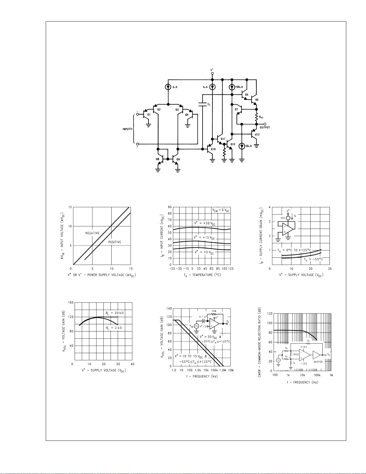
Schematic Diagram (Each Amplifier)
LM124/LM224/LM324/LM2902
Typical Performance Characteristics
DS009299-2
Input Voltage Range
Voltage Gain
DS009299-34
Input Current
Open Loop Frequency
Response
DS009299-35
Supply Current
DS009299-36
Common Mode Rejection
Ratio
DS009299-37
www.national.com 6
DS009299-38
DS009299-39
 Loading...