

NSC LM25574MT, LM25574 Datasheet
March 2007
LM25574
SIMPLE SWITCHER® 42V, 0.5A Step-Down Switching
Regulator
General Description
The LM25574 is an easy to use SIMPLE SWITCHER® buck
regulator which allows design engineers to design and optimize a robust power supply using a minimum set of components. Operating with an input voltage range of 6 - 42V, the
LM25574 delivers 0.5A of continuous output current with an
integrated 750mΩ N-Channel MOSFET. The regulator utilizes an Emulated Current Mode architecture which provides
inherent line regulation, tight load transient response, and
ease of loop compensation without the usual limitation of lowduty cycles associated with current mode regulators. The
operating frequency is adjustable from 50kHz to 1MHz to allow optimization of size and efficiency. To reduce EMI, a
frequency synchronization pin allows multiple IC’s from the
LM(2)557x family to self-synchronize or to synchronize to an
external clock. The LM25574 guarantees robustness with cycle-by-cycle current limit, short-circuit protection, thermal
shut-down, and remote shut-down. The device is available in
a TSSOP-16 package. The LM25574 is supported by the full
suite of WEBENCH® On-Line design tools.
Features
■
Integrated 42V, 750mΩ N-channel MOSFET
■
Ultra-wide input voltage range from 6V to 42V
■
Adjustable output voltage as low as 1.225V
■
1.5% feedback reference accuracy
■
Operating frequency adjustable between 50kHz and
1MHz with single resistor
■
Master or slave frequency synchronization
■
Adjustable soft-start
■
Emulated current mode control architecture
■
Wide bandwidth error amplifier
■
Built-in protection
Package
■
TSSOP-16
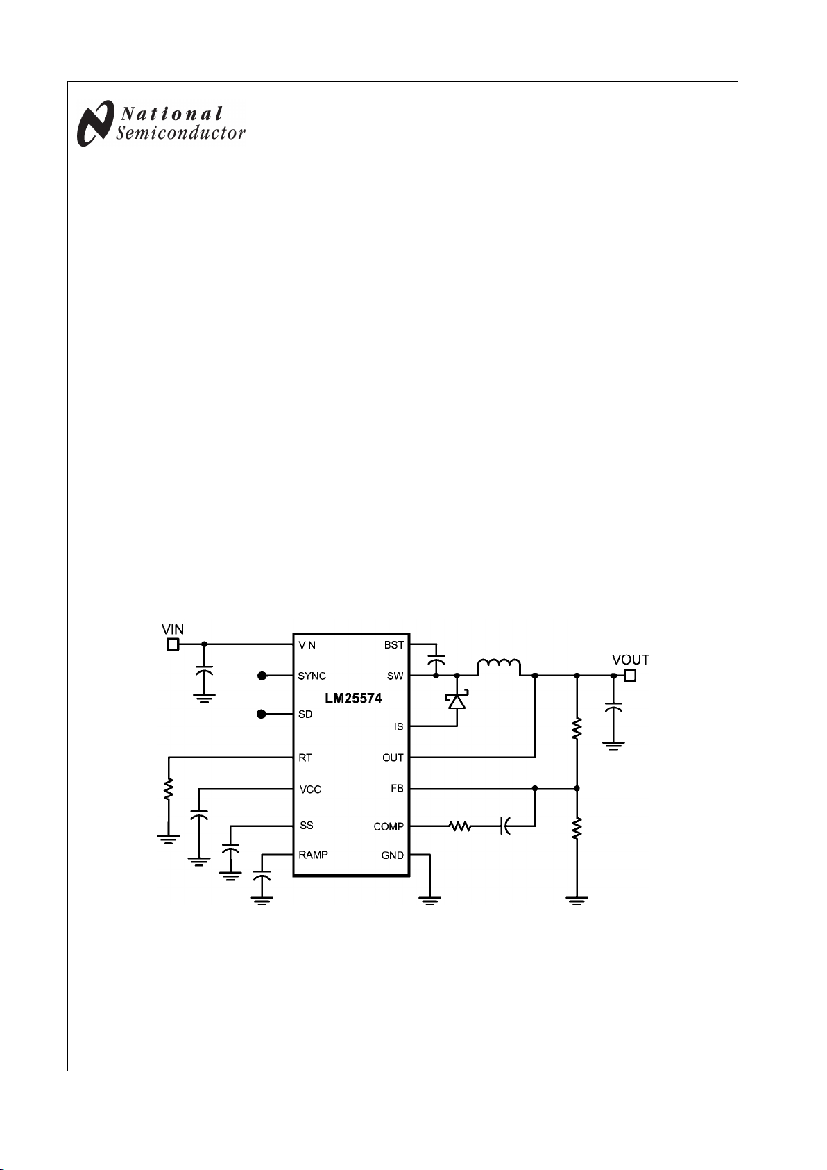
Simplified Application Schematic
20214101
WEBENCH® is a registered trademark of National Semiconductor Corporation.
© 2007 National Semiconductor Corporation 202141 www.national.com
LM25574 SIMPLE SWITCHER® 42V, 0.5A Step-Down Switching Regulator
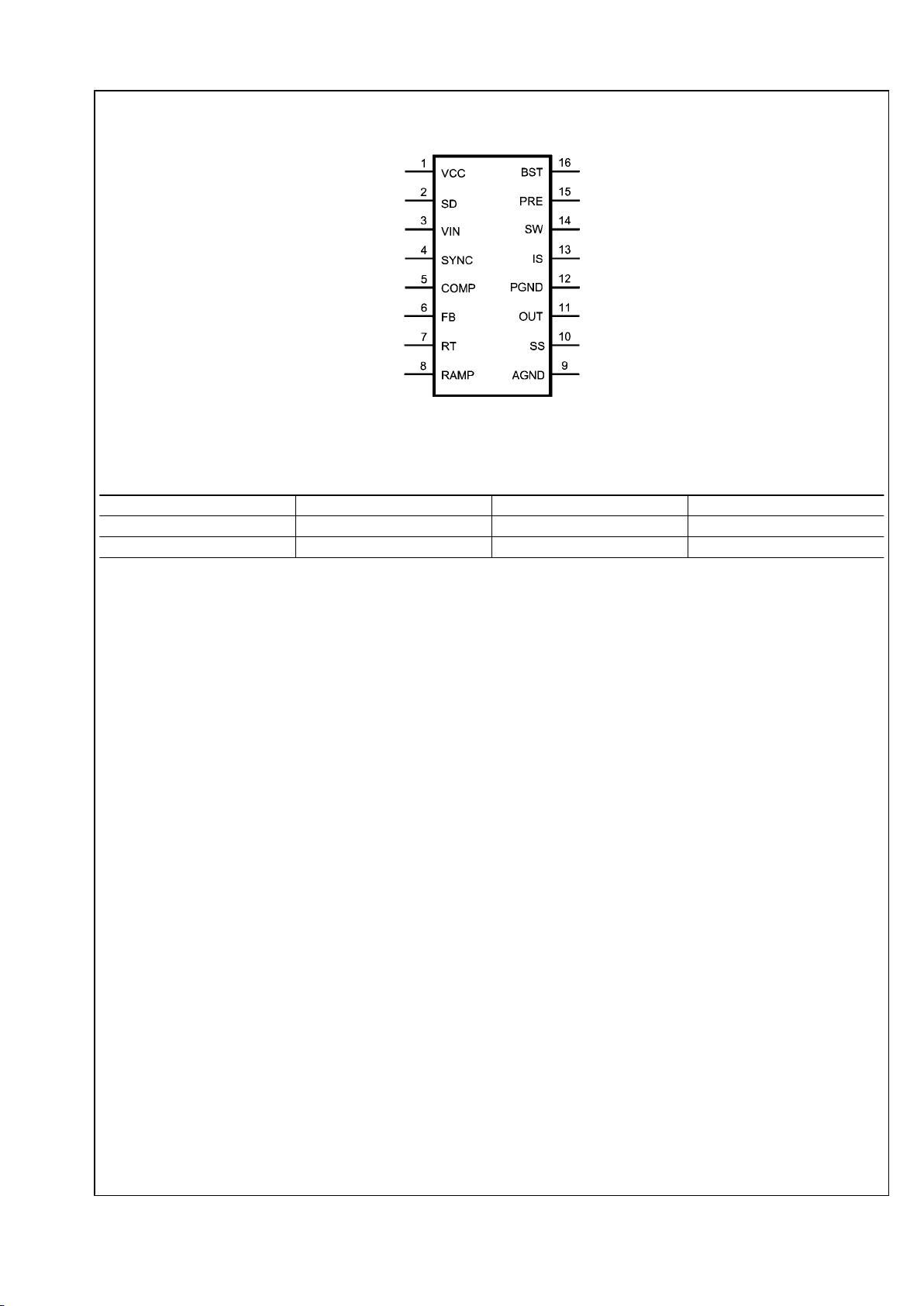
Connection Diagram
20214102
Top View
16-Lead TSSOP
Ordering Information
Order Number Package Type NSC Package Drawing Supplied As
LM25574MT TSSOP-16 MTC16 92 Units in Rail
LM25574MTX TSSOP-16 MTC16 2500 Units on Tape and Reel
www.national.com 2
LM25574
Pin Descriptions
Pin(s) Name Description Application Information
1 VCC Output of the bias regulator Vcc tracks Vin up to 9V. Beyond 9V, Vcc is regulated to 7
Volts. A 0.1uF to 1uF ceramic decoupling capacitor is
required. An external voltage (7.5V – 14V) can be applied
to this pin to reduce internal power dissipation.
2 SD Shutdown or UVLO input If the SD pin voltage is below 0.7V the regulator will be in a
low power state. If the SD pin voltage is between 0.7V and
1.225V the regulator will be in standby mode. If the SD pin
voltage is above 1.225V the regulator will be operational. An
external voltage divider can be used to set a line
undervoltage shutdown threshold. If the SD pin is left open
circuit, a 5µA pull-up current source configures the regulator
fully operational.
3 Vin Input supply voltage Nominal operating range: 6V to 42V
4 SYNC Oscillator synchronization input or output The internal oscillator can be synchronized to an external
clock with an external pull-down device. Multiple LM25574
devices can be synchronized together by connection of their
SYNC pins.
5 COMP Output of the internal error amplifier The loop compensation network should be connected
between this pin and the FB pin.
6 FB Feedback signal from the regulated
output
This pin is connected to the inverting input of the internal
error amplifier. The regulation threshold is 1.225V.
7 RT Internal oscillator frequency set input The internal oscillator is set with a single resistor, connected
between this pin and the AGND pin.
8 RAMP Ramp control signal An external capacitor connected between this pin and the
AGND pin sets the ramp slope used for current mode
control. Recommended capacitor range 50pF to 2000pF.
9 AGND Analog ground Internal reference for the regulator control functions
10 SS Soft-start An external capacitor and an internal 10µA current source
set the time constant for the rise of the error amp reference.
The SS pin is held low during standby, Vcc UVLO and
thermal shutdown.
11 OUT Output voltage connection Connect directly to the regulated output voltage.
12 PGND Power ground Low side reference for the PRE switch and the IS sense
resistor.
13 IS Current sense Current measurement connection for the re-circulating
diode. An internal sense resistor and a sample/hold circuit
sense the diode current near the conclusion of the off-time.
This current measurement provides the DC level of the
emulated current ramp.
14 SW Switching node The source terminal of the internal buck switch. The SW pin
should be connected to the external Schottky diode and to
the buck inductor.
15 PRE Pre-charge assist for the bootstrap
capacitor
This open drain output can be connected to SW pin to aid
charging the bootstrap capacitor during very light load
conditions or in applications where the output may be precharged before the LM25574 is enabled. An internal precharge MOSFET is turned on for 250ns each cycle just prior
to the on-time interval of the buck switch.
16 BST Boost input for bootstrap capacitor An external capacitor is required between the BST and the
SW pins. A 0.022µF ceramic capacitor is recommended.
The capacitor is charged from Vcc via an internal diode
during the off-time of the buck switch.
3 www.national.com
LM25574
Absolute Maximum Ratings (Note 1)
If Military/Aerospace specified devices are required,
please contact the National Semiconductor Sales Office/
Distributors for availability and specifications.
VIN to GND 45V
BST to GND 60V
PRE to GND 45V
SW to GND (Steady State) -1.5V
BST to V
CC
45V
SD, VCC to GND 14V
BST to SW 14V
OUT to GND Limited to Vin
SYNC, SS, FB, RAMP to GND 7V
ESD Rating (Note 2)
Human Body Model 2kV
Storage Temperature Range -65°C to +150°C
Operating Ratings (Note 1)
V
IN
6V to 42V
Operation Junction Temperature −40°C to + 125°C
Electrical Characteristics Specifications with standard typeface are for T
J
= 25°C, and those with boldface type
apply over full Operating Junction Temperature range. VIN = 24V, RT = 32.4kΩ unless otherwise stated. (Note 3)
Symbol Parameter Conditions Min Typ Max Units
STARTUP REGULATOR
VccReg Vcc Regulator Output 6.85 7.15 7.45 V
Vcc LDO Mode turn-off 9 V
Vcc Current Limit Vcc = 0V 25 mA
VCC SUPPLY
Vcc UVLO Threshold (Vcc increasing) 5.03 5.35 5.67 V
Vcc Undervoltage Hysteresis 0.35 V
Bias Current (Iin) FB = 1.3V 3.7 4.5 mA
Shutdown Current (Iin) SD = 0V 48 70 µA
SHUTDOWN THRESHOLDS
Shutdown Threshold (SD Increasing) 0.47 0.7 0.9 V
Shutdown Hysteresis 0.1 V
Standby Threshold (Standby Increasing) 1.17 1.225 1.28 V
Standby Hysteresis 0.1 V
SD Pull-up Current Source 5 µA
SWITCH CHARACTERSICS
Buck Switch Rds(on) 750 1500
mΩ
BOOST UVLO 4 V
BOOST UVLO Hysteresis 0.56 V
Pre-charge Switch Rds(on) 70
Ω
Pre-charge Switch on-time 250 ns
CURRENT LIMIT
Cycle by Cycle Current Limit RAMP = 0V 0.6 0.7 0.8 A
Cycle by Cycle Current Limit Delay RAMP = 2.5V 75 ns
SOFT-START
SS Current Source 7 10 14 µA
OSCILLATOR
Frequency1 180 200 220 kHz
Frequency2
RT = 11kΩ
425 485 545 kHz
SYNC Source Impedance 11
kΩ
SYNC Sink Impedance 110
Ω
SYNC Threshold (falling) 1.3 V
SYNC Frequency
RT = 11kΩ
550 kHz
SYNC Pulse Width Minimum 15 ns
www.national.com 4
LM25574
Symbol Parameter Conditions Min Typ Max Units
RAMP GENERATOR
Ramp Current 1 Vin = 36V, Vout=10V 272 310 368 µA
Ramp Current 2 Vin = 10V, Vout=10V 36 50 64 µA
PWM COMPARATOR
Forced Off-time 416 500 575 ns
Min On-time 80 ns
COMP to PWM Comparator Offset 0.7 V
ERROR AMPLIFIER
Feedback Voltage Vfb = COMP 1.207 1.225 1.243 V
FB Bias Current 17 nA
DC Gain 70 dB
COMP Sink / Source Current 3 mA
Unity Gain Bandwidth 3 MHz
DIODE SENSE RESISTANCE
D
SENSE
250
mΩ
THERMAL SHUTDOWN
Tsd Thermal Shutdown Threshold 165 °C
Thermal Shutdown Hysteresis 25 °C
THERMAL RESISTANCE
θ
JC
Junction to Case 30 °C/W
θ
JA
Junction to Ambient 90 °C/W
Note 1: Absolute Maximum Ratings are limits beyond which damage to the device may occur. Operating Ratings are conditions under which operation of the
device is intended to be functional. For guaranteed specifications and test conditions, see the Electrical Characteristics.
Note 2: The human body model is a 100pF capacitor discharged through a 1.5kΩ resistor into each pin.
Note 3: Min and Max limits are 100% production tested at 25°C. Limits over the operating temperature range are guaranteed through correlation using Statistical
Quality Control (SQC) methods. Limits are used to calculate National’s Average Outgoing Quality Level (AOQL).
Typical Performance Characteristics
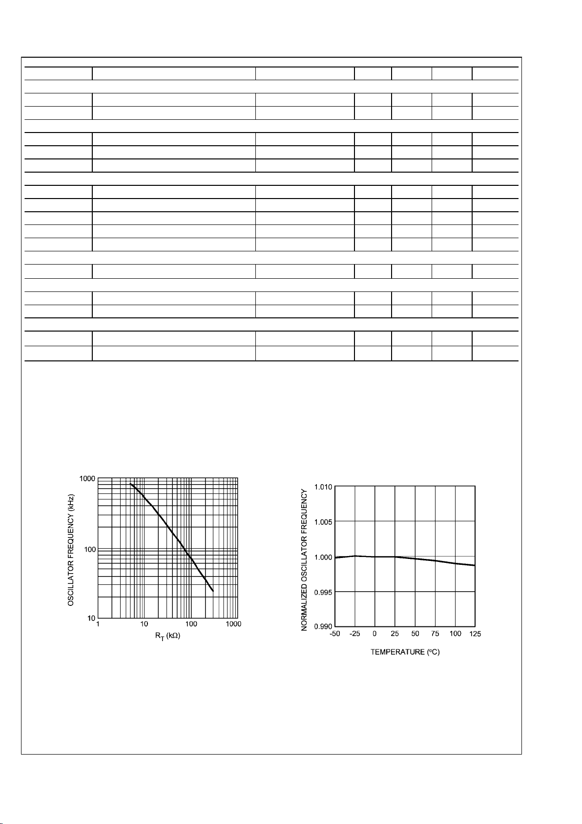
Oscillator Frequency vs R
T
20214120
Oscillator Frequency vs Temperature
F
OSC
= 200kHz
20214121
5 www.national.com
LM25574
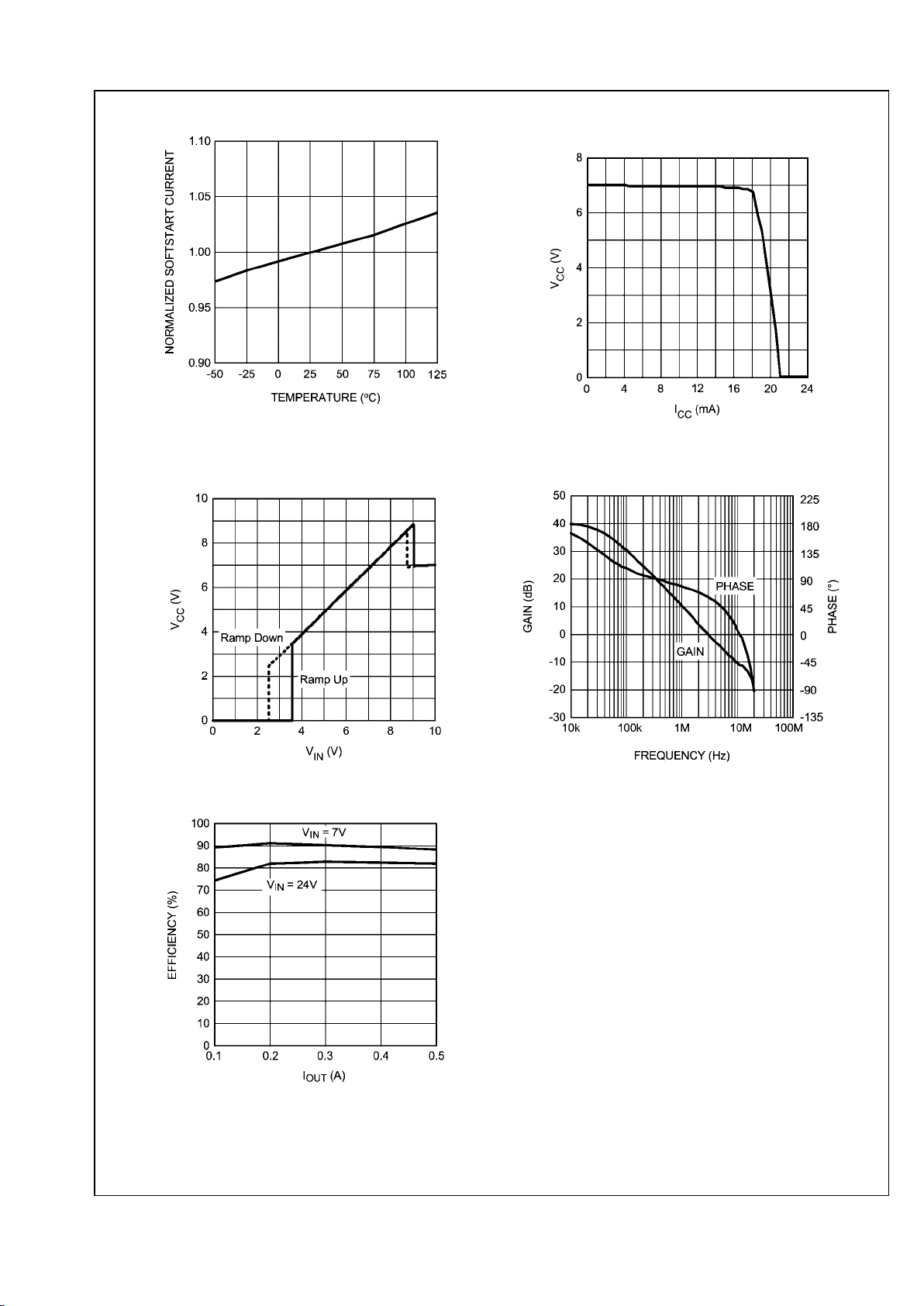
Soft Start Current vs Temperature
20214122
VCC vs I
CC
VIN = 12V
20214123
VCC vs V
IN
RL = 7kΩ
20214124
Error Amplifier Gain/Phase
A
VCL
= 101
20214125
Demoboard Efficiency vs I
OUT
and V
IN
20214126
www.national.com 6
LM25574
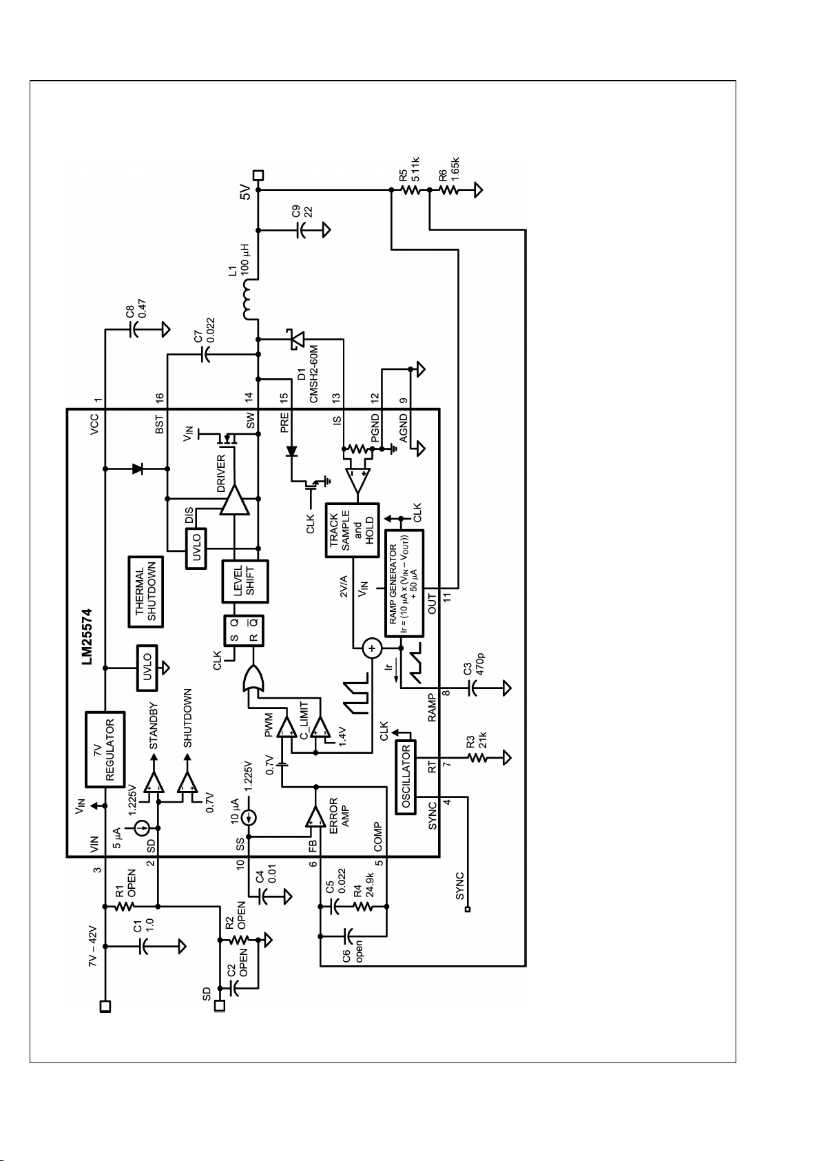
Typical Application Circuit and Block Diagram
20214103
FIGURE 1.
7 www.national.com
LM25574
 Loading...