LM2427
Triple 80 MHz CRT Driver
LM2427 Triple 80 MHz CRT Driver
April 1995
General Description
The LM2427 is a high performance triple CRT driver for
simplifying color monitor designs. The device contains three
large signal transimpedance amplifiers, and provides direct
cathode drive capability. A plastic power package and pinto-pin compatibility make the LM2427 ideal for new designs
or as a low cost replacement for designs using the LH2426
or CR5527.
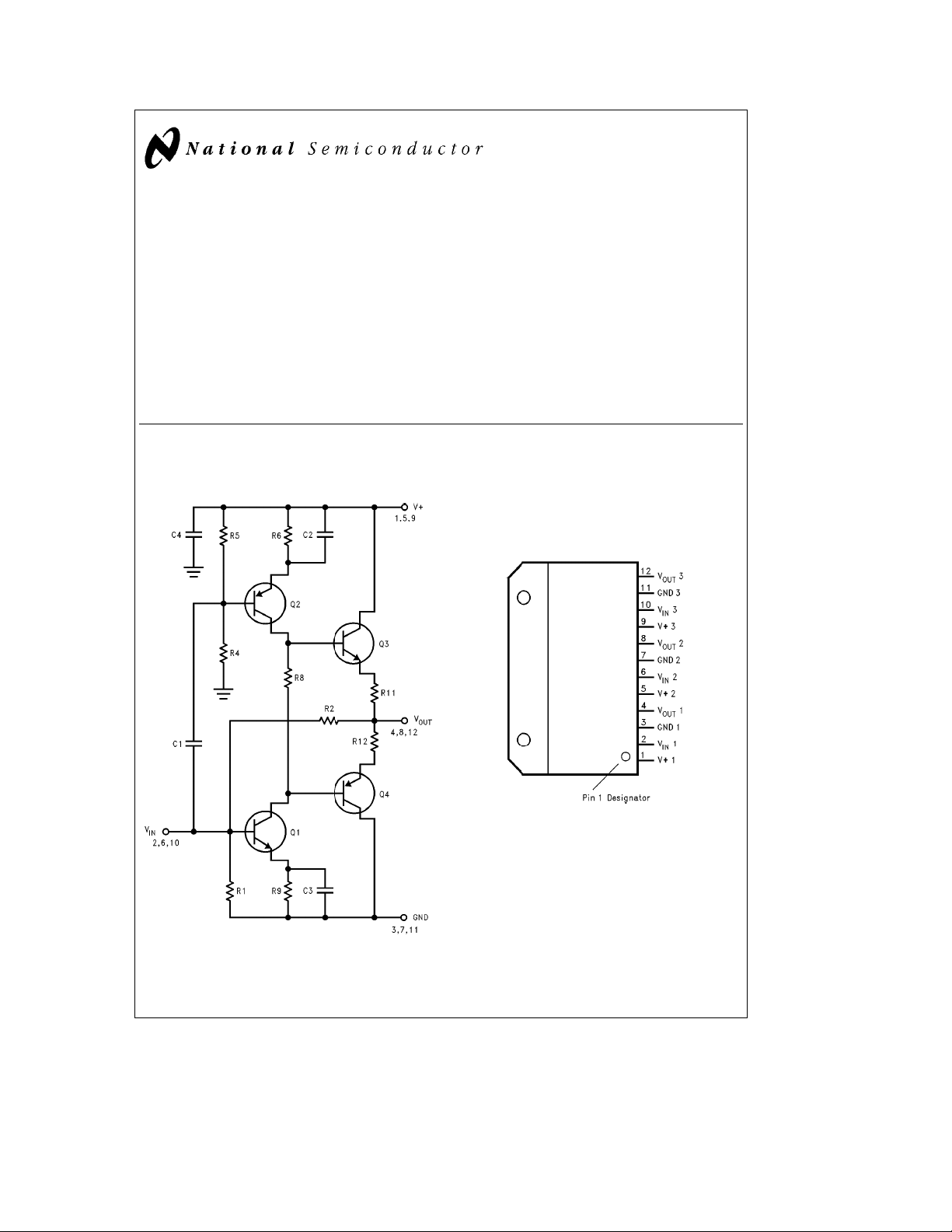
Schematic and Connection Diagrams
(One Section)
Features
Y
Low-cost plastic power package
Y
Typical rise/fall times of 3.5 ns
Y
80 MHz video bandwidth at 50 VPPwith 8 pF load
Y
Operation from 80V power supply
Applications
Y
CRT driver for color monitors
Y
Drives CRT cathode directly
Y
Pin-to-pin compatible with the LH2426 and CR5527
CRT drivers
Top View
Order Number LM2427T
See NS Package Number MKT-TA12A
TL/H/11967– 1
C
1995 National Semiconductor Corporation RRD-B30M115/Printed in U. S. A.
TL/H/11967
TL/H/11967– 2

Absolute Maximum Ratings
If Military/Aerospace specified devices are required,
please contact the National Semiconductor Sales
Office/Distributors for availability and specifications.
Supply Voltage, V
Safe Operating Power Consumption 14W
aa
85V
CASE
b
25§Ctoa100§C
b
20§Ctoa90§C
Storage Temperature Range, T
Operating Temperature Range, T
STG
Lead Temperature (Soldering, 10 sec.) 300§C
ESD Tolerance TBD
Electrical Characteristics V
offset. See
Figure 1.
T
e
25§C unless otherwise noted.
CASE
ae
80V, R
e
430X,C1e47 pF, C
G
Symbol Parameter Conditions
I
CC
V
INDC
V
OUTDC
t
R
t
F
A
V
LE Linearity Error V
DA
V
Note 1: Input signal: tr,t
Note 2: Linearity error is defined as: The variation in small signal gain from
Note 3: Calculated value from voltage gain test on each channel.
Supply Current (per Amplifier) No Input or Output Load 24 30 mA
Input Offset Voltage 1.4 1.6 1.8 V
Output Offset Voltage 34 40 46 V
Rise Time 10% to 90% (Note 1) 3.5 ns
Fall Time 90% to 10% (Note 1) 3.5 ns
Voltage Gain
froma10V toa70V (Note 2) 5 %
OUT
Gain Matching (Note 3) 0.2 dB
k
f
1.5 ns, f
e
1 MHz.
in
a
20V toa70V output with a 100 mVAC, 1 MHz, input signal.
Typical Performance Characteristics
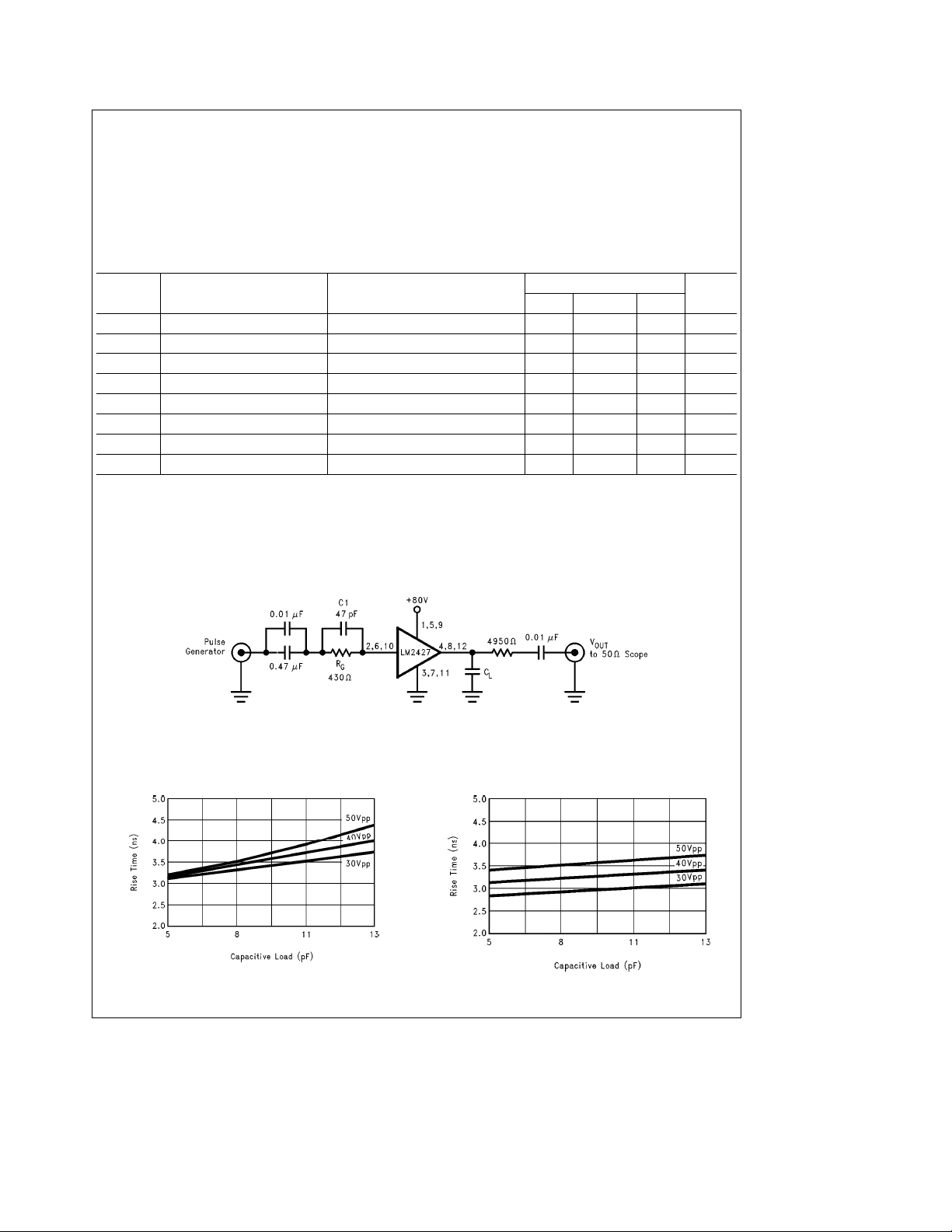
Typical Test Circuit (One Section)
e
8 pF, 50 VPPoutput swing with 40V DC
L
LM2427
Min Typical Max
b
b
11
b
13
14 V/V
Units
Note: CL, total load capacltance, includes all parasitic capacitances.
FIGURE 1. Test Circuit (One Section)
This test circuit is used for both characteristic plots.
Typical Rise Time vs Capacitive Loading
TL/H/11967– 10
TL/H/11967– 3
Typical Fall Time vs Capacitive Loading
TL/H/11967– 5
2
 Loading...