

LM2419
Triple 65 MHz CRT Driver
LM2419 Triple 65 MHz CRT Driver
December 1994
General Description
The LM2419 contains three wide bandwidth, large signal
amplifiers designed for large voltage swings. The amplifiers
have a gain of
CRT monitors and is a low cost solution to designs conforming to 1024 x 768 display resolution.
The device is mounted in the industry standard 11-lead
TO-220 molded power package. The heat sink is electrically
isolated and may be grounded for ease of manufacturing
and EMI/RFI shielding.
b
15. The device is intended for use in color
Schematic and Connection Diagrams
One Channel
Features
Y
50 VPPoutput swing at 65 MHz
Y
Rise/Fall time 5 ns with 12 pF load
Y
60 VPPoutput swing capability
Y
Pin and function compatible with LM2416
Y
No low frequency tilt compensation required
Applications
Y
CRT driver for SVGA, IBM 8514 and 1024 x 768
display resolution RGB monitors
TL/H/11442– 1
Order Number LM2419T
See NS Package Number TA11B
C
1995 National Semiconductor Corporation RRD-B30M115/Printed in U. S. A.
TL/H/11442
TL/H/11442– 2

Absolute Maximum Ratings (Note 1)
If Military/Aerospace specified devices are required,
please contact the National Semiconductor Sales
Office/Distributors for availability and specifications.
Supply Voltage (V
Storage Temperature (T
Operating Case Temperature, T
Lead Temperature (solderingk10 sec.) 300§C
ESD Tolerance 2 kV
a
)
)
STG
Case
b
25§Ctoa100§C
b
a
85V
20§Ctoa90§C
Electrical Characteristics
Unless otherwise specified, the following specifications apply for V
swing; frequency
Symbol Parameter Conditions
I
CC
I
B
V
OUT
t
r
t
f
A
V
OS Overshoot VIN:tr,t
LE Linearlty Error V
e
1 MHz; V
Bias
e
12V; C
L
e
12 pF; T
A
Supply Current (per Amplifier) Input/Output Open Circuit 27 40 mA
Bias Current (Pins 2 or 7 or 9) 11 mA
Output Offset Voltage 40 50 60 V
Rise Time 10% to 90% 5 ns
Fall Time 90% to 10% 5 ns
Voltage Gain
k
f
e
25V to 75V 8 %
OUT
a
e
e
25§C; see test circuit,
80V, DC input bias, V
Figure 1
.
IN DC
e
3.9V; 50 VPPoutput
Min Typ Max Units
(Note 3) (Note 2) (Note 3) (Limit)
b
13
b
15
b
18 V/V
2ns 8 %
DAVmatch Gain Matching 0.3 dB
Note 1: Absolute Maximum Ratings indicate limits beyond which damage to the device may occur. The guaranteed specifications apply only for the test conditions
listed. Some performance characteristics may degrade when the device is not operated under the listed test conditions.
Note 2: Typical specifications are at 25
Note 3: Min/Max limits are guaranteed to National’s AOQL (Average Outgoing Quality Level).
C and represent the most likely parametric norm.
§
Typical Performance
Characteristics
e
T
25§C, Test CircuitÐ
A
Figure 1
Frequency Response
*12 pF is the total load capacitance and includes the test fixture capacitance.
TL/H/11442– 3
FIGURE 1. Test Circuit (One Section)
TL/H/11442– 4
2

Typical Performance
Characteristics
e
T
25§C, Test CircuitÐ
A
Pulse Response
(Continued)
Figure 1
small signal cross over distortion. Resistor R3 is used to
prevent Q2 from oscillating at high frequencies.
TL/H/11442– 5
Test Circuit
Figure 1
LM2419. The input signal is AC coupled into the input of
LM2419 and is referenced to 3.9V DC using an external
3.9V DC bias through a 390X resistor. The test circuit is
designed to allow testing of the LM2419 in a 50X environment such as a 50X oscilloscope or network analyzer. The
4950X resistor in series with the output of the LM2419
forms a 100:1 voltage divider when connected to a 50X
oscilloscope or network analyzer.
shows a typical test circuit for evaluation of the
Theory of Operation
The LM2419 is a high voltage triple CRT driver suitable for
SVGA, IBM 8514 and 1024 x 768 display resolution monitors. The device is packaged in the industry standard
11 lead TO-220 molded power package. The heat sink is
electrically isolated and may be grounded for ease of manufacturing and RFl/EMl shielding.
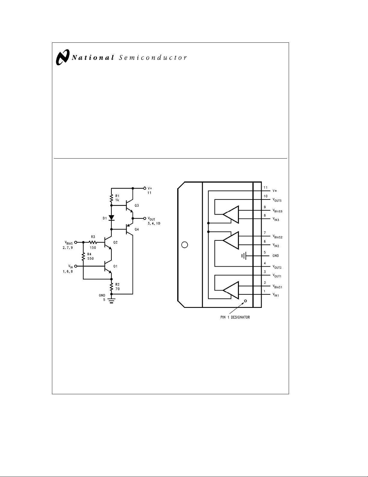
The schematic diagram of LM2419 is shown in
and R2 provide a conversion of the input voltage to current
while Q2 acts as a common base amplifier to drive the load
resistor, R1. Resistor R4 along with R2 sets up the DC bias
at the base of Q1. Emitter followers Q3 and Q4 isolate R1
from the capacitive load at the output, thus making the rise
and fall times relatively insensitive to the load capacitance.
The gain of the amplifier is
approximately
limited by the time constant due to R1 and the capacitances
associated with D1, Q2, Q3 and Q4. Diode D1 is used to
provide some bias voltage for Q3 and Q4 so as to reduce
b
15. The bandwidth of LM2419 is primarily
b
R1/(R2llR4) and is fixed at
Figure 2
.Q1
FIGURE 2. Schematic Diagram of
One Section of LM2419
TL/H/11442– 7
Application Hints
POWER SUPPLY BYPASS
Since the LM2419 is a wide-bandwidth amplifier with greater
than 10,000 V/ms slew rate, proper power supply bypassing
is critical for optimum performance. Improper power supply
bypassing can result in large overshoot, ringing and oscillation. A 0.01 mF ceramic capacitor should be connected as
close to the supply pin as is practical (preferably less than
(/4
from the supply pin). The lead length of the 0.01 mF
×
ceramic capacitor should be as small as is practical. In addition, 10 mF–100 mF electrolytic capacitor should be connected from the supply pin to ground. The electrolytic capacitor should be placed reasonably close to the LM2419’s
supply pin.
ARC PROTECTION
The LM2419 must be protected from arcing within the CRT.
To limit the arcover voltage, a 200V spark gap is recommended at the cathode. Clamp diodes D1 and D2 (as
shown in
output of LM2419 to a safe level. The clamp diodes used
should have high current rating, low series impedance and
low shunt capacitance. Resistor R2 in
arcover current while R1 limits the current into LM2419 and
reduces the power dissipation of the output transistors
when the output is stressed beyond the supply voltage.
Having large value resistors for R1 and R2 would be desirable but this has the effect of reducing rise and fall times.
Figure 3
) are used to clamp the voltage at the
Figure 3
limits the
3
 Loading...