

NSC LM2412T Datasheet

LM2412
Monolithic Triple 2.8 ns CRT Driver
General Description
The LM2412 is an integrated high voltage CRT driver circuit
designed for use in high resolution color monitor applications. The IC contains three high input impedance, wide
band amplifiers which directly drive the RGB cathodes of a
CRT. Each channelhas its gain internally set to −14 and can
drive CRT capacitive loads as well as resistive loads presented by other applications, limited only by the package’s
power dissipation. The LM2412 is a low power alternative of
the LM2402
The IC is packaged in an industry standard 11 lead TO-220
molded plastic power package. See thermal considerations
section for heat sinking requirements.
Features
n Rise/fall times typically 2.8 ns with 8 pF load at 40 V
Schematic and Connection Diagrams
n Lower power than LM2402 with the same bandwidth
n Well matched with LM2202 video preamps
n Output swing capability: 50 V
n 1V to 5V input range
n Stable with 0-20 pF capacitive loads and inductive
peaking networks
n Convenient TO-220 staggered lead package style
n Standard LM240X family pinout which is designed for
easy PCB layout
Applications
n CRT driver for color monitors with display resolutions up
to 1600 x 1200 with 85 Hz refresh rate
n Pixel clock frequency up to 200 MHz
PP
LM2412 Monolithic Triple 2.8 ns CRT Driver
December 1999
=
for V
PP
80V
CC
DS101298-1
FIGURE 1. Simplified Schematic Diagram
(One Channel)
© 1999 National Semiconductor Corporation DS101298 www.national.com
Top View
Order Number LM2412T
See NS package Number
DS101298-2
Absolute Maximum Ratings (Notes 1, 2)
If Military/Aerospace specified devices are required,
LM2412
please contact the National Semiconductor Sales Office/
Distributors for availability and specifications.
Supply Voltage, V
Bias Voltage, V
Input Voltage, V
Storage Temperature Range, T
Lead Temperature (Soldering,
CC
BB
IN
−65˚C to +150˚C
STG
<
10 sec.) 300˚C
+90V
+16V
0V to 6V
ESD Tolerance
Human Body Model 2 kV
Machine Model 250V
Operating Ranges (Note 3)
V
CC
V
BB
V
IN
V
OUT(VCC
=
80V, V
=
12V) +15V to +75V
BB
+60V to +85V
+8V to +15V
Case Temperature −20˚C to +100˚C
Do not operate the part without a heat sink.
Electrical Characteristics
(See
Figure 2
Unless otherwise noted: V
for Test Circuit)
Symbol Parameter Conditions
I
I
V
A
∆A
CC
BB
OUT
V
V
Supply Current Per Channel, No Output Load 16 21 26 mA
Bias Current All Three Channels 27 42 57 mA
DC Output Voltage V
DC Voltage Gain −12 −14 −16
Gain Matching (Note 4) 1.0 dB
LE Linearity Error (Notes 4, 5) 3.5
t
r
t
f
Rise Time (Notes 6, 7) 10%to 90%,40VPPOutput (1 MHz) 2.8 3.5 ns
Fall Time (Notes 6, 7) 10%to 90%,40VPPOutput (1 MHz) 2.8 3.5 ns
OS Overshoot 40 V
Note 1: “Absolute Maximum Ratings” are those values beyond which the safety of the device cannot be guaranteed. They are not meant to imply that the devices
should be operated at these limits. The table of “Electrical Characteristics” specifies conditions of device operation.
Note 2: All voltages are measured with respect to GND, unless otherwise specified.
Note 3: Operating ratings indicate conditions for which the device is functional, but do not guarantee specific performance limits. For guaranteed specifications and
test conditions, see the Electrical Characteristics. The guaranteed specifications apply only for the test conditions listed. Some performance characteristics may
change when the device is not operated under the listed test conditions.
Note 4: Calculated value from voltage gain test on each channel.
Note 5: Linearity error is the variation in DC gain from V
Note 6: Input from signal generator: t
Note 7: 100%tested in production. These limits are not used to calculate outgoing quality levels.
=
+80V, V
CC
BB
=
+12V, V
=
+3.3 V
IN
DC,CL
=
8 pF, T
=
60˚C, no AC input.
C
LM2412
Min Typ Max
=
1.9V 62 65 68 V
IN
Output (1 MHz) 5
PP
r,tf
=
<
1 ns.
IN
1.6V to V
=
5.0V.
IN
+1V to +5V
Units
DC
%
%
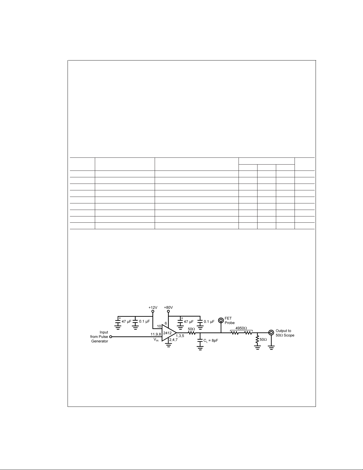
AC Test Circuit
FIGURE 2. Test Circuit (One Channel)
Figure 2
shows a typical test circuit for evaluation of the
LM2412. This circuit is designed to allow testing of the
LM2412 in a 50Ω environment without the use of an expensive FET probe. The combined resitors of 4950Ω at the output form a 200:1 voltage divider when connected to a 50Ω
load. The test board supplied by NSC also offers the option
to test theLM2412 with a FET probe. C
www.national.com 2
is the total capaci-
L
DS101298-3
tance at the LM2412 output, including the board capacitance.

Typical Performance Characteristics
LM2412
FIGURE 3. VINvs V
OUT
FIGURE 4. Speed vs Temp.
DS101298-4
DS101298-6
DS101298-5
FIGURE 6. Power Dissipation vs Frequency
DS101298-7
FIGURE 7. Speed vs Offset
FIGURE 5. Rise/Fall Time
DS101298-8
DS101298-9
FIGURE 8. Bandwidth
www.national.com3

Theory of Operation
The LM2412 is a high voltage monolithic three channel CRT
LM2412
driver suitable for very high resolution display applications,
up to 1600 x 1200 at 85 Hz refresh rate. The LM2412 operates using 80V and 12V power supplies. The part is housed
in the industry standard 11-lead TO-220 molded plastic
power package.
The simplified circuit diagram of one channel of the LM2412
is shown in
Figure 1
.APNP emitter follower,Q5, provides input buffering. This minimizes the current loading of the video
pre-amp. R9 is used to turn on Q5 when there is no input.
With Q5 turned on, Q1 will be almost completely off, minimizing the current flow through Q1 and Q2. This will drive the
output stage near the V
tion with no inputs. R6 is a pull-up resistor for Q5 and also
rail, minimizing the power dissipa-
CC
limits the current flow through Q5. R3 and R2 are used to set
the current flow through Q1 and Q2. The ratio of R1 to R2 is
used to set the gain of the LM2412. R1, R2 and R3 are all related when calculating the output voltage of the CRT driver.
R
limits the current through the base of Q2. Q1 and Q2 are
b
in a cascode configuration. Q1 is a low voltage and very fast
transistor. Q2 is a higher voltage transistor. The cascode
configuration gives the equivalent of a very fast and high
voltage transistor. The two output transistors, Q3 and Q4,
form a class B amplifier output stage. R4 and R5 are used to
limit the current through the output stage and set the output
impedance of the LM2412. Q6, along with R7 and R8 set the
bias current through Q3 and Q4 when there is no change in
the signal level. This bias current minimizes the crossover
distortion of the output stage. With this bias current the output stage now becomes a class AB amplifier with a crossover distortion much lower than a class B amplifier.
Figure 2
shows a typical test circuit for evaluation of the
LM2412. Due to the very wide bandwidth of the LM2412, it is
highly recommended that the stand alone board suplied by
NSC be used for the evaluation of the CRT driver’s performance. The 50Ω resistor is used to duplicate the required
series resistor in the actual application. This resistor would
be part of the arc-over protection circuit. The input signal
from the generator is AC coupled to the input of the CRT
driver.
Application Hints
shoot, ringing and oscillation. A 0.1 µF capacitor should be
connected from the supply pin, V
the supply and ground pins as is practical. Additionally, a
, to ground, as close to
CC
10 µF to 100 µF electrolytic capacitor should be connected
from the supply pin to ground. The electrolytic capacitor
should also be placed reasonably close to the LM2412’s
supply and ground pins. A 0.1 µF capacitor should be connected from the bias pin, V
tical to the part.
, to ground, as close as is prac-
BB
ARC PROTECTION
During normal CRT operation, internal arcing may occasionally occur. Spark gaps, in the range of 200V,connected from
the CRT cathodes to CRT groundwill limit the maximum voltage, but to a value that is much higher than allowable on the
LM2412. This fast, high voltage, high energy pulse can damage the LM2412 output stage. The application circuit shown
in
Figure 9
is designed to help clamp the voltage at the output of the LM2412 to a safe level. The clamp diodes should
have a fast transient response, high peak current rating, low
series impedance and low shunt capacitance. FDH400 or
equivalent diodes are recommended. D1 and D2 should
have short, low impedance connections to V
respectively.The cathode of D1 should be located very close
and ground
CC
to a separately decoupled bypass capacitor. The ground
connection of the diode and the decoupling capacitor should
be very close to the LM2412 ground.This will significantly reduce the high frequency voltage transients that the LM2412
would be subjected to during an arc-over condition. Resistor
R2 limits the arc-over current that is seen by the diodes while
R1 limits the current into the LM2412 as well as the voltage
stress at the outputs of the device. R2 should be a
carbon type resistor. R1 can be a
1
⁄4W metal or carbon film
1
⁄2W solid
type resistor. Inductor L1 is critical to reduce the initial high
frequency voltage levels that the LM2412 would be subjected to during an arc-over. Having large value resistors for
R1 and R2 would be desirable, but this has the effect of increasing rise and fall times. The inductor will not only help
protect the device but it will also help optimize rise and fall
times as well as minimize EMI. For proper arc protection, it is
important to not omit any of the arc protection components
shown in
Figure 9
. The values of L1 and R1 may need to be
adjusted for a particular application.The recommended minimum value for R1 is 75Ω, with L1=.049 µH.
INTRODUCTION
National Semiconductor (NSC) is committed to providing application information that assists our customers in obtaining
the best performance possible fromour products. The following information is provided in order to support this commitment. The reader should be aware that the optimization of
performance was done using a specific printed circuit board
designed at NSC. Variations in performance can be realized
due to physical changes in the printed circuit board and the
application. Therefore, the designer should know that component value changes may be required in order to optimize
performance in a given application. The values shown in this
document can be used as a starting point for evaluation purposes. When working with high bandwidth circuits, good layout practices are also critical to achieving maximum performance.
POWER SUPPLY BYPASS
Since the LM2412 is a very high bandwidth amplifier, proper
power supply bypassing is critical for optimum performance.
Improper power supply bypassing can result in large over-
www.national.com 4
DS101298-10
FIGURE 9. One Channel of the LM2412 with the
Recommended Arc Protection Circuit.
OPTIMIZING TRANSIENT RESPONSE
Figure 9
Referring to
, there are three components (R1, R2
and L1) that can be adjusted to optimize the transient response of the application circuit. Increasing the values of R1
and R2 will slow the circuit down while decreasing overshoot. Increasing the value of L1 will speed up the circuit as
well as increase overshoot. It is very important to use inductors with very high self-resonant frequencies, preferably
 Loading...