

NSC LM2403T Datasheet
LM2403
Monolithic Triple 4.5 nS CRT Driver
LM2403 Monolithic Triple 4.5 nS CRT Driver
August 1999
General Description
The LM2403 is an integrated high voltage CRT driver circuit
designed for use in high resolution color monitor applications. The IC contains three high input impedance, wide
band amplifiers which directly drive the RGB cathodes of a
CRT. Each channelhas its gain internally set to −14 and can
drive CRT capacitive loads as well as resistive loads presented by other applications, limited only by the package’s
power dissipation.
The IC is packaged in an industry standard 11 lead TO-220
molded plastic power package. See thermal considerations
on page 5.
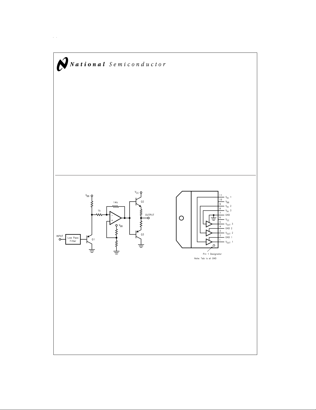
Schematic and Connection Diagrams
Features
n Rise/fall times typically 4.5 nS with 8 pF load at 40 V
n Well matched with LM1283 video preamp
n Output swing capability: 60 V
n 1V to 5V input range
n Stable with 0 pF–20 pF capacitive loads and inductive
peaking networks
n Convenient TO-220 staggered lead package style
n Standard LM240X Family Pinout which is designed for
easy PCB layout
for VCC= 80V
pp
pp
Applications
n CRT driver for color monitors with display resolutions up
to 1600 x 1200
n Pixel clock frequency up to 160 MHz
DS100082-1
Top View
Order Number LM2403T
FIGURE 1. Simplified Schematic Diagram (One Channel)
© 1999 National Semiconductor Corporation DS100082 www.national.com
DS100082-2

Absolute Maximum Ratings (Notes 1, 2)
If Military/Aerospace specified devices are required,
please contact the National Semiconductor Sales Office/
Distributors for availability and specifications.
Supply Voltage (V
Bias Voltage (V
Input Voltage (V
Storage Temperature Range (T
Lead Temperature
(Soldering,
ESD Tolerance, Human Body Model 2 kV
Machine Model 250V
) +90V
CC
) +16V
BB
) −0.5V to V
IN
<
10 sec.) 300˚C
) −65˚C to +150˚C
STG
BIAS
+0.5V
Operating Range(Note 3)
V
CC
V
BB
V
IN
V
OUT
Case Temperature −20˚C to +100˚C
Do not operate the part without a heat sink.
Note 1: Absolute Maximum Ratings indicate limits beyond which damage to
the device may occur.
Note 2: All voltages are measured with respect to GND, unless otherwise
specified.
Note 3: Operating ratings indicate conditions for which the device is functional, but do not guarantee specific performance limits. For guaranteed
specifications and test conditions, see the Electrical Characteristics. The
guaranteed specifications apply only for the test conditions listed. Some performance characteristics may change when the device is not operated under
the listed test conditions.
+60V to +85V
+8V to +15V
+1V to +5V
+10V to +70V
Electrical Characteristics
(See
Figure 2
Unless otherwise noted: VCC= +80V, VBB= +12 V, VIN= +3.3 VDC,CL= 8 pF, LP= 0.22 µH, Output = 40 VPPat 1 MHz, TA=
25˚C.
Symbol Parameter Condition
I
CC
I
BB
V
OUT
A
V
∆A
V
LE Linearity Error (Notes 4, 5), No AC Input Signal 3.5
t
R
t
F
OS Overshoot 3
Note 4: Calculated value from Voltage Gain test on each channel.
Note 5: Linearity Error is the variation in dc gain from V
Note 6: Input from signal generator: t
for Test Circuit)
LM2403
Min Typical Max
Units
Supply Current Per Channel, No Output Load 26 mA
Bias Current All Three Channels 11.5 mA
DC Output Voltage No AC Input Signal, VIN= 2.8 V 48 52 56 V
DC Voltage Gain No AC Input Signal −12 −14 −16
Gain Matching (Note 4), No AC Input Signal 1.0 dB
Rise Time 10%to 90
Fall Time 90%to 10
1 nS.
IN
r,tf
<
%
%
= 1.5V to VIN=5V.
4.5 nS
4.5 nS
DC
%
%
AC Test Circuit
DS100082-3
FIGURE 2. Test Circuit (One Channel)
Figure 2
shows a typical test circuit for evaluation of the LM2403. This circuit is designed to allow testing of the LM2403 in a 50Ω
environment without the use of an expensive FET probe. The 4950Ω resistor at the output forms a 100:1 voltage divider when
connected to a 50Ω load.
www.national.com 2

AC Test Circuit (Continued)
FIGURE 3. V
OUT
vs V
DS100082-4
IN
DS100082-7
FIGURE 6. Power Dissipation vs Frequency
FIGURE 4. Speed vs Temp.
DS100082-6
FIGURE 5. Pulse Response
DS100082-5
DS100082-8
FIGURE 7. Speed vs Offset
DS100082-9
FIGURE 8. Pulse Response with VCC=70V
www.national.com3
DC

Theory of Operation
The LM2403 is a high voltage monolithic three channel CRT
driver suitable for high resolution display applications. The
LM2403 operates using 80V and 12V power supplies. The
part is housed in the industry standard 11-lead TO-220
molded plastic power package.
The simplified circuit diagram of the LM2403 is shown in
ure 1
. A PNP emitter follower, Q1, provides input buffering.
The 14 kΩ feedback resistor and the 1 kΩ input resistor sets
the gain of the inverting op-amp to -14. Emitter followers Q2
and Q3 isolate the output of the feedback amplifier from the
capacitance of the CRT cathode, and make the circuit relatively insensitive to load capacitance.
Figure 2
LM2403. This circuit is designed to allow testing of the
LM2403 in a 50Ω environment without the use of an expensive FET probe. In this test circuit, two low inductance resistors in series totaling 4.95 kΩ form a 100:1 wideband low capacitance probe when connected to a 50Ω cable and load.
The input signal from the generator is ac coupled to the base
of Q1.
Figure 9
sponse of the LM2403. The frequency response rolls off very
rapidly above the bandwidth limit of the amplifier. There are
two reasons for this fast response roll-off:
1. The LM2403 contains an input low pass filter to help re-
2. The internal feedback network of the closed loop ampli-
In both cases, the fast roll of the high frequency harmonics
will help to limit the creation of high frequency EMI harmonics, without limiting video rise and fall time characteristics.
However, due to the very fast switching speeds of the de-
shows a typical test circuit for evaluation of the
DS100082-16
FIGURE 9.
shows the large signal sine wave frequency re-
move unwanted high frequency harmonics that can
cause EMI problems. This filter does not significantly affect the rise and fall times of the signal as it operates
above the −3 dB bandwidth of the device.
fier holds the gain at −14 until the loop gain drops below
unity. Above this frequency, the amplifier response falls
with the open loop gain of the amplifier, as the feedback
ceases to have any significant effect. There is also a
change in the impedance match between the op-amp
and the emitter follower output stage with large signals
at higher frequencies. This creates a gain boost that extends the bandwidth, then gives a sudden roll off as
shown in
may vary slightly depending upon operating conditions,
signal amplitude etc.
Figure 9
. The exact response of this roll off
Fig-
vice, good layout design for EMI is CRITICAL. Path lengths
and loop areas of the video signals must be kept to a minimum.
Application Hints
INTRODUCTION
National Semiconductor (NSC) is committed to providing application information that assists our customers in obtaining
the best performance possible fromour products. The following information is provided in order to support this commitment. The reader should be aware that the optimization of
performance was done using a specific printed circuit board
designed at NSC. Variations in performance can be realized
due to physical changes in the printed circuit board and the
application. Therefore, the designer should know that component value changes may be required in order to optimize
performance in a given application. The values shown in this
document can be used as a starting point for evaluation purposes. When working with high bandwidth circuits, good layout practices are also critical to achieving maximum performance.
POWER SUPPLY BYPASS
Since the LM2403 is a high bandwidth amplifier, proper
power supply bypassing is critical for optimum performance.
Improper power supply bypassing can result in large overshoot, ringing and oscillation. A 0.1 µF capacitor should be
connected from the supply pin, Vcc, to ground, as close to
the supply and ground pins as is practical. Additionally, a
10 µF to 100 µF electrolytic capacitor should be connected
from the supply pin to ground. The electrolytic capacitor
should also be placed reasonably close to the LM2403’s
supply and ground pins. A 0.1µF capacitor should be connected from the bias pin, Vbb, to ground, as close as is practical to the part.
ARC PROTECTION
During normal CRT operation, internal arcing may occasionally occur. Spark gaps, in the range of 200V,connected from
the CRT cathodes to CRT groundwill limit the maximum voltage, but to a value that is much higher than allowable on the
LM2403. This fast, high voltage, high energy pulse can damage the LM2403 output stage. The application circuit shown
in
Figure 10
put of the LM2403 to a safe level. The clamp diodes should
have a fast transient response, high peak current rating, low
series impedance and low shunt capacitance. FDH400 or
equivalent diodes are recommended. D1 and D2 should
have short, low impedance connections to V
respectively.The cathode of D1 should be located very close
to a separately decoupled bypass capacitor. The ground
connection of the diode and the decoupling capacitor should
be very close to the LM2403 ground.This will significantly reduce the high frequency voltage transients that the LM2403
would be subjected to during an arcover condition. Resistor
R2 limits the arcover current that is seen by the diodes while
R1 limits the current into the LM2403 as well as the voltage
stress at the outputs of the device. R2 should be a 1/2W
solid carbon type resistor.R1 can be a 1/4W metal or carbon
film type resistor. Inductor L1 is critical to reduce the initial
high frequency voltage levels that the LM2403 would be subjected to. Having large value resistors for R1 and R2 would
be desirable, but this has the effect of increasing rise and fall
times. The inductor will not only help protect the device but it
is designed to help clamp the voltage at the out-
and ground
CC
www.national.com 4
 Loading...