NSC LM12H458MWG-883, LM12H458MEL-883, LM12H458CIVF, LM12H458CIV Datasheet

LM12454/LM12458/LM12H458
12-Bit + Sign Data Acquisition System with
Self-Calibration
General Description
The LM12454, LM12458, and LM12H458 are highly integrated Data Acquisition Systems. Operating on just 5V, they
combine a fully-differential self-calibrating (correcting linearity and zero errors) 13-bit (12-bit + sign) analog-to-digital
converter (ADC) and sample-and-hold (S/H) with extensive
analog functions and digital functionality. Up to 32 consecutive conversions, using two’s complement format, can be
stored in an internal 32-word (16-bit wide) FIFO data buffer.
An internal 8-word RAM can store the conversion sequence
for up to eight acquisitions through the LM12(H)458’s
eight-input multiplexer. The LM12454 has a four-channel
multiplexer,a differential multiplexer output, and a differential
S/H input. The LM12454 and LM12(H)458 can also operate
with 8-bit + sign resolution and in a supervisory “watchdog”
mode that compares an input signal against two programmable limits.
Programmable acquisition times and conversion rates are
possible through the use of internal clock-driven timers. The
reference voltage input can be externally generated for absolute or ratiometric operation or can be derived using the internal 2.5V bandgap reference.
All registers, RAM, and FIFO are directly addressable
through the high speed microprocessor interface to either an
8-bit or 16-bit databus. The LM12454 and LM12(H)458 include a direct memory access (DMA) interface for
high-speed conversion data transfer.
An evaluation/interface board is available. Order number LM12458EVAL.
Additional applications information can be found in applications notes AN-906, AN-947 and AN-949.
Key Specifications
(f
CLK
=
5 MHz; 8 MHz, H)
j
Resolution 12-bit + sign or 8-bit + sign
j
13-bit conversion time 8.8 µs, 5.5 µs (H) (max)
j
9-bit conversion time 4.2 µs, 2.6 µs (H) (max)
j
13-bit Through-put rate 88k samples/s (min),
140k samples/s (H) (min)
j
Comparison time
(“watchdog” mode)
2.2 µs (max),
1.4 µs (H) (max)
j
ILE
±
1 LSB (max)
j
VINrange GND to V
A
+
j
Power dissipation 30 mW, 34 mW (H) (max)
j
Stand-by mode 50 µW (typ)
j
Single supply 3V to 5.5V
Features
n Three operating modes: 12-bit + sign, 8-bit + sign, and
“watchdog”
n Single-ended or differential inputs
n Built-in Sample-and-Hold and 2.5V bandgap reference
n Instruction RAM and event sequencer
n 8-channel (LM12(H)458), 4-channel (LM12454)
multiplexer
n 32-word conversion FIFO
n Programmable acquisition times and conversion rates
n Self-calibration and diagnostic mode
n 8- or 16-bit wide databus dmicroprocessor or DSP
interface
Applications
n Data Logging
n Instrumentation
n Process Control
n Energy Management
n Inertial Guidance
TRI-STATE®is a registered trademark of National Semiconductor Corporation.
AT
®
is a registered trademark of International Business Machines Corporation.
July 1999
LM12454/LM12458/LM12H458
12-Bit + Sign Data Acquisition System with Self-Calibration
© 1999 National Semiconductor Corporation DS011264 www.national.com
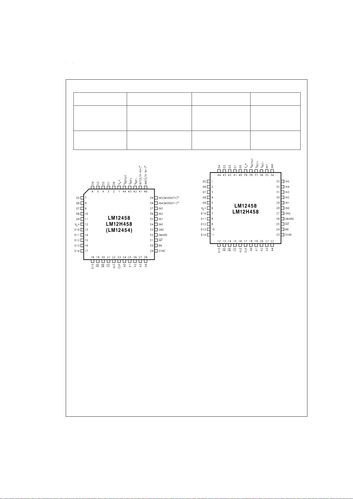
Ordering Information
Guaranteed Guaranteed Order See NS
Clock Freq (min) Linearity Error (max) Part Number Package Number
8 MHz
±
1.0 LSB LM12H458CIV V44A
LM12H458CIVF VGZ44A
LM12H458MEL/883 EL44A
or 5962-9319502MYA
5 MHz
±
1.0 LSB LM12454CIV V44A
LM12458CIV V44A
LM12458CIVF VGZ44A
Connection Diagrams
DS011264-2
* Pin names in ( ) apply to the LM12454 and LM12H454.
Order Number LM12454CIV,
LM12458CIV or LM12H458CIV
See NS Package Number V44A
Order Number LM12H458MEL/883 or 5962-9319502MYA
See NS Package Number EL44A
DS011264-34
Order Number LM12458CIVF or LM12H458CIVF
See NS Package Number VGZ44A
www.national.com 2
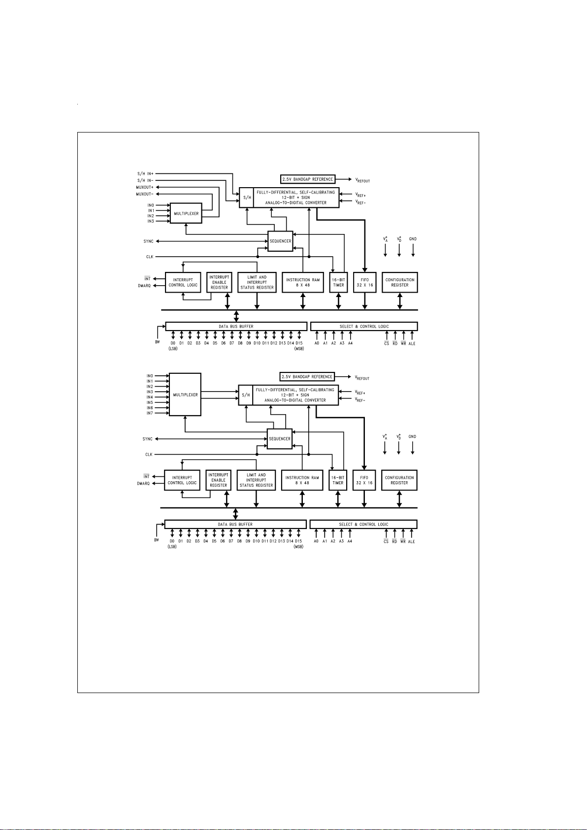
Functional Diagrams
LM12454
DS011264-1
LM12(H)458
DS011264-21
www.national.com3
Absolute Maximum Ratings (Notes 1, 2)
If Military/Aerospace specified devices are required,
please contact the National Semiconductor Sales Office/
Distributors for availability and specifications.
Supply Voltage (V
A
+ and VD+) 6.0V
Voltage at Input and Output Pins
except IN0–IN3 (LM12454) −0.3V to V
+
+ 0.3V
and IN0–IN7 (LM12(H)458)
Voltage at Analog Inputs IN0–IN3 (LM12454)
and IN0–IN7 (LM12(H)458) GND − 5V to V
+
+5V
|V
A
+−VD+| 300 mV
Input Current at Any Pin (Note 3)
±
5mA
Package Input Current (Note 3)
±
20 mA
Power Dissipation (T
A
=
25˚C)
V Package (Note 4) 875 mW
Storage Temperature −65˚C to +150˚C
Lead Temperature
V Package, Infrared, 15 sec. +300˚C
EL and W Packages,
Solder, 10 sec. +250˚C
ESD Susceptibility (Note 5) 1.5 kV
LM12458MEL/883 2.0 kV
See AN-450 “Surface Mounting Methods and Their Effect on
Product Reliability” for other methods of soldering surface
mount devices.
Operating Ratings (Notes 1, 2)
Temperature Range
(T
min
≤ TA≤ T
max
)
LM12454CIV/
LM12(H)458CIV −40˚C ≤ T
A
≤ 85˚C
LM12458MEL/883 −55˚C ≤ T
A
≤ 125˚C
Supply Voltage
V
A
+, VD+ 3.0V to 5.5V
|V
A
+−VD+| ≤100 mV
V
IN+
Input Range GND ≤ V
IN+
≤ VA+
V
IN−
Input Range GND ≤ V
IN−
≤ VA+
V
REF+
Input Voltage 1V ≤ V
REF+
≤ VA+
V
REF−
Input Voltage 0V ≤ V
REF−
≤ V
REF+
−1V
V
REF+−VREF−
1V ≤ V
REF
≤ VA+
V
REF
Common Mode
Range (Note 16) 0.1 V
A
+
≤ V
REFCM
≤ 0.6 V
A
+
Converter Characteristics (Notes 6, 7, 8, 9, 19)
The following specifications apply to the LM12454, LM12458, and LM12H458 for VA+=VD+=5V, V
REF+
=
5V, V
REF−
=
0V,
12-bit + sign conversion mode, f
CLK
=
8.0 MHz (LM12H458) or f
CLK
=
5.0 MHz (LM12454/8), R
S
=
25Ω, source impedance for
V
REF+
and V
REF−
≤ 25Ω, fully-differential input with fixed 2.5V common-mode voltage, and minimum acquisition time unless
otherwise specified. Boldface limits apply for T
A
=
T
J
=
T
MIN
to T
MAX
; all other limits T
A
=
T
J
=
25˚C.
Symbol Parameter Conditions Typical Limits Unit
(Note 10) (Note 11) (Limit)
ILE Positive and Negative Integral After Auto-Cal (Notes 12, 17)
±
1/2
±
1 LSB (max)
Linearity Error
TUE Total Unadjusted Error After Auto-Cal (Note 12)
±
1 LSB
Resolution with No Missing Codes After Auto-Cal (Note 12) 13 Bits (max)
DNL Differential Non-Linearity After Auto-Cal
±
3
⁄
4
LSB (max)
Zero Error After Auto-Cal (Notes 13, 17)
±
1
LM12H458
±
1/2
±
1.5 LSB (max)
Positive Full-Scale Error After Auto-Cal (Notes 12, 17)
±
1/2
±
2 LSB (max)
LM12(H)458MEL
±
2.5
Negative Full-Scale Error After Auto-Cal (Notes 12, 17)
±
1/2
±
2 LSB (max)
LM12(H)458MEL
±
2.5
DC Common Mode Error (Note 14)
±
2
±
3.5 LSB (max)
ILE 8-Bit + Sign and “Watchdog” (Note 12)
Mode Positive and Negative
±
1/2 LSB (max)
Integral Linearity Error
TUE 8-Bit + Sign and “Watchdog” Mode After Auto-Zero
±
1/2
±
3/4 LSB (max)
Total Unadjusted Error
8-Bit + Sign and “Watchdog” Mode 9 Bits (max)
Resolution with No Missing Codes
DNL 8-Bit + Sign and “Watchdog” Mode
±
3/4 LSB (max)
Differential Non-Linearity
8-Bit + Sign and “Watchdog” Mode After Auto-Zero
±
1/2 LSB (max)
Zero Error
8-Bit + Sign and “Watchdog” Positive
±
1/2 LSB (max)
and Negative Full-Scale Error
www.national.com 4
Converter Characteristics (Notes 6, 7, 8, 9, 19) (Continued)
The following specifications apply to the LM12454, LM12458, and LM12H458 for VA+=VD+=5V, V
REF+
=
5V, V
REF−
=
0V,
12-bit + sign conversion mode, f
CLK
=
8.0 MHz (LM12H458) or f
CLK
=
5.0 MHz (LM12454/8), R
S
=
25Ω, source impedance for
V
REF+
and V
REF−
≤ 25Ω, fully-differential input with fixed 2.5V common-mode voltage, and minimum acquisition time unless
otherwise specified. Boldface limits apply for T
A
=
T
J
=
T
MIN
to T
MAX
; all other limits T
A
=
T
J
=
25˚C.
Symbol Parameter Conditions Typical Limits Unit
(Note 10) (Note 11) (Limit)
8-Bit + Sign and “Watchdog” Mode
±
1/8 LSB
DC Common Mode Error
Multiplexer Channel-to-Channel
±
0.05 LSB
Matching
V
IN+
Non-Inverting Input Range GND V (min)
V
A
+ V (max)
V
IN−
Inverting Input Range GND V (min)
V
A
+ V (max)
V
IN+−VIN−
Differential Input Voltage Range −V
A
+
V (min)
V
A
+ V (max)
Common Mode Input Voltage Range GND V (min)
V
A
+ V (max)
PSS Power Supply Zero Error V
A
+=VD+=5V±10
%
±
0.2
±
1.75 LSB (max)
Sensitivity Full-Scale Error V
REF+
=
4.5V, V
REF−
=
GND
±
0.4
±
2 LSB (max)
(Note 15) Linearity Error
±
0.2 LSB
C
REF
V
REF+/VREF−
Input Capacitance 85 pF
C
IN
Selected Multiplexer Channel Input 75 pF
Capacitance
Converter AC Characteristics (Notes 6, 7, 8, 9, 19)
The following specifications apply to the LM12454, LM12458, and LM12H458 for VA+=VD+=5V, V
REF+
=
5V, V
REF−
=
0V,
12-bit + sign conversion mode, f
CLK
=
8.0 MHz (LM12H458) or f
CLK
=
5.0 MHz (LM12454/8), R
S
=
25Ω, source impedance for
V
REF+
and V
REF−
≤ 25Ω, fully-differential input with fixed 2.5V common-mode voltage, and minimum acquisition time unless
otherwise specified. Boldface limits apply for T
A
=
T
J
=
T
MIN
to T
MAX
; all other limits T
A
=
T
J
=
25˚C.
Symbol Parameter Conditions Typical Limits Unit
(Note 10) (Note 11) (Limit)
Clock Duty Cycle 50
%
40
%
(min)
60
%
(max)
t
C
Conversion Time 13-Bit Resolution, 44 (t
CLK
) 44 (t
CLK
)+50ns (max)
Sequencer State S5 (
Figure 15
)
9-Bit Resolution, 21 (t
CLK
) 21 (t
CLK
)+50ns (max)
Sequencer State S5 (
Figure 15
)
t
A
Acquisition Time Sequencer State S7 (
Figure 15
)9(t
CLK
) 9(t
CLK
)+50ns (max)
Built-in minimum for 13-Bits
Built-in minimum for 9-Bits and 2 (t
CLK
) 2(t
CLK
)+50ns (max)
“Watchdog” mode
t
Z
Auto-Zero Time Sequencer State S2 (
Figure 15
)76(t
CLK
) 76 (t
CLK
)+50ns (max)
t
CAL
Full Calibration Time Sequencer State S2 (
Figure 15
) 4944 (t
CLK
) 4944 (t
CLK
)+50ns (max)
Throughput Rate 89 88 kHz
(Note 18) LM12H458 142 140 (min)
t
WD
“Watchdog” Mode Comparison Sequencer States S6, S4, 11 (t
CLK
) 11 (t
CLK
)+50ns (max)
Time and S5 (
Figure 15
)
www.national.com5
Converter AC Characteristics (Notes 6, 7, 8, 9, 19) (Continued)
The following specifications apply to the LM12454, LM12458, and LM12H458 for VA+=VD+=5V, V
REF+
=
5V, V
REF−
=
0V,
12-bit + sign conversion mode, f
CLK
=
8.0 MHz (LM12H458) or f
CLK
=
5.0 MHz (LM12454/8), R
S
=
25Ω, source impedance for
V
REF+
and V
REF−
≤ 25Ω, fully-differential input with fixed 2.5V common-mode voltage, and minimum acquisition time unless
otherwise specified. Boldface limits apply for T
A
=
T
J
=
T
MIN
to T
MAX
; all other limits T
A
=
T
J
=
25˚C.
Symbol Parameter Conditions Typical Limits Unit
(Note 10) (Note 11) (Limit)
DSNR Differential Signal-to-Noise Ratio V
IN
=
±
5V
f
IN
=
1 kHz 77.5 dB
f
IN
=
20 kHz 75.2 dB
f
IN
=
40 kHz 74.7 dB
SESNR Single-Ended Signal-to-Noise V
IN
=
5V
p-p
Ratio f
IN
=
1 kHz 69.8 dB
f
IN
=
20 kHz 69.2 dB
f
IN
=
40 kHz 66.6 dB
DSINAD Differential Signal-to-Noise + V
IN
=
±
5V
Distortion Ratio f
IN
=
1 kHz 76.9 dB
f
IN
=
20 kHz 73.9 dB
f
IN
=
40 kHz 70.7 dB
SESINAD Single-Ended Signal-to-Noise + V
IN
=
5V
p-p
Distortion Ratio f
IN
=
1 kHz 69.4 dB
f
IN
=
20 kHz 68.3 dB
f
IN
=
40 kHz 65.7 dB
DTHD Differential Total Harmonic V
IN
=
±
5V
Distortion f
IN
=
1 kHz −85.8 dB
f
IN
=
20 kHz −79.9 dB
f
IN
=
40 kHz −72.9 dB
SETHD Single-Ended Total Harmonic V
IN
=
5V
p-p
Distortion f
IN
=
1 kHz −80.3 dB
f
IN
=
20 kHz −75.6 dB
f
IN
=
40 kHz −72.8 dB
DENOB Differential Effective Number V
IN
=
±
5V
of Bits f
IN
=
1 kHz 12.6 Bits
f
IN
=
20 kHz 12.2 Bits
f
IN
=
40 kHz 12.1 Bits
SEENOB Single-Ended Effective Number V
IN
=
5V
p-p
of Bits f
IN
=
1 kHz 11.3 Bits
f
IN
=
20 kHz 11.2 Bits
f
IN
=
40 kHz 10.8 Bits
DSFDR Differential Spurious Free V
IN
=
±
5V
Dynamic Range f
IN
=
1 kHz 87.2 dB
f
IN
=
20 kHz 78.9 dB
f
IN
=
40 kHz 72.8 dB
Multiplexer Channel-to-Channel V
IN
=
5V
PP
Crosstalk f
IN
=
40 kHz
LM12454 MUXOUT Only −76 dB
LM12(H)458 MUX −78 dB
plus Converter
t
PU
Power-Up Time 10 ms
t
WU
Wake-Up Time 10 ms
www.national.com 6
DC Characteristics (Notes 6, 7, 8, 19)
The following specifications apply to the LM12454, LM12458, and LM12H458 for VA+=VD+=5V, V
REF+
=
5V, V
REF−
=
0V,
f
CLK
=
8.0 MHz (LM12H454/8) or f
CLK
=
5.0 MHz (LM12458), and minimum acquisition time unless otherwise specified. Bold-
face limits apply for T
A
=
T
J
=
T
MIN
to T
MAX
; all other limits T
A
=
T
J
=
25˚C.
Symbol Parameter Conditions Typical Limits Unit
(Note 10) (Note 11) (Limit)
I
D
+VD+ Supply Current CS=“1”
LM12454/8 0.55 1.0 mA (max)
LM12H458 0.55 1.2
I
A
+VA+ Supply Current CS=“1”
LM12454/8 3.1 5.0 mA (max)
LM12H458 3.1 5.5
I
ST
Stand-By Supply Current (ID++IA+) Power-Down Mode Selected
Clock Stopped 10 µA (max)
8 MHz Clock 40 µA (max)
Multiplexer ON-Channel Leakage Current V
A
+=5.5V
ON-Channel=5.5V 0.3
OFF-Channel=0V 0.1 µA (max)
LM12(H)458MEL 0.5
ON-Channel=0V 0.3
OFF-Channel=5.5V 0.1 µA (max)
LM12(H)458MEL 0.5
Multiplexer OFF-Channel Leakage Current V
A
+=5.5V
ON-Channel=5.5V 0.3
OFF-Channel=0V 0.1 µA (max)
LM12(H)458MEL 0.5
ON-Channel=0V 0.3
OFF-Channel=5.5V 0.1 µA (max)
LM12(H)458MEL 0.5
R
ON
Multiplexer ON-Resistance LM12454
V
IN
=
5V 800 1500 Ω(max)
V
IN
=
2.5V 850 1500 Ω(max)
V
IN
=
0V 760 1500 Ω(max)
Multiplexer Channel-to-Channel LM12454
R
ON
matching V
IN
=
5V
±
1.0
%
±
3.0
%
(max)
V
IN
=
2.5V
±
1.0
%
±
3.0
%
(max)
V
IN
=
0V
±
1.0
%
±
3.0
%
(max)
Internal Reference Characteristics (Notes 6, 7, 19)
The following specifications apply to the LM12454, LM12458, and LM12H458 for VA+=VD+=5V unless otherwise specified.
Boldface limits apply for T
A
=
T
J
=
T
MIN
to T
MAX
; all other limits T
A
=
T
J
=
25˚C.
Symbol Parameter Conditions Typical Limits Unit
(Note 10) (Note 11) (Limit)
V
REFOUT
Internal Reference Output Voltage 2.5 2.5±4
%
V (max)
LM12(H)458MEL 2.5
±
6
%
∆V
REF
/∆T Internal Reference Temperature 40 ppm/˚C
Coefficient
∆
REF
/∆ILInternal Reference Load Regulation Sourcing (0<IL≤ +4 mA) 0.2
%
/mA (max)
Sinking (−1 ≤ I
IL
<
0 mA) 1.2
%
/mA (max)
∆V
REF
Line Regulation 4.5V ≤ VA+ ≤ 5.5V 3 20 mV (max)
I
SC
Internal Reference Short Circuit Current V
REFOUT
=
0V 13 25 mA (max)
∆V
REF
/∆t Long Term Stability 200 ppm/kHr
www.national.com7
Internal Reference Characteristics (Notes 6, 7, 19) (Continued)
The following specifications apply to the LM12454, LM12458, and LM12H458 for VA+=VD+=5V unless otherwise specified.
Boldface limits apply for T
A
=
T
J
=
T
MIN
to T
MAX
; all other limits T
A
=
T
J
=
25˚C.
Symbol Parameter Conditions Typical Limits Unit
(Note 10) (Note 11) (Limit)
t
SU
Internal Reference Start-Up Time VA+=VD+=0V→5V 10 ms
C
L
=
100 µF
Digital Characteristics (Notes 6, 7, 8, 19)
The following specifications apply to the LM12454, LM12458, and LM12H458 for VA+=VD+=5V, unless otherwise specified. Boldface limits apply for T
A
=
T
J
=
T
MIN
to T
MAX
; all other limits T
A
=
T
J
=
25˚C.
Symbol Parameter Conditions Typical Limits Unit
(Note 10) (Note 11) (Limit)
V
IN(1)
Logical “1” Input Voltage VA+=VD+=5.5V 2.0 V (min)
V
IN(0)
Logical “0” Input Voltage VA+=VD+=4.5V 0.8 V (max)
I
IN(1)
Logical “1” Input Current V
IN
=
5V 0.005 1.0 µA (max)
LM12(H)458MEL 2.0
I
IN(0)
Logical “0” Input Current V
IN
=
0V −0.005 −1.0 µA (max)
LM12(H)458MEL −2.0
C
IN
D0–D15 Input Capacitance 6 pF
V
OUT(1)
Logical “1” Output Voltage VA+=VD+=4.5V
I
OUT
=
−360 µA 2.4 V (min)
I
OUT
=
−10 µA 4.25 V (min)
V
OUT(0)
Logical “0” Output Voltage VA+=VD+=4.5V 0.4 V (max)
I
OUT
=
1.6 mA
I
OUT
TRI-STATE®Output Leakage Current V
OUT
=
0V −0.01 −3.0 µA (max)
V
OUT
=
5V 0.01 3.0 µA (max)
Digital Timing Characteristics (Notes 6, 7, 8, 19)
The following specifications apply to the LM12454, LM12458, and LM12H458 for VA+=VD+=5V, t
r
=
t
f
=
3 ns, and C
L
=
100 pF on data I/O, INT and DMARQ lines unless otherwise specified. Boldface limits apply for T
A
=
T
J
=
T
MIN
to T
MAX
; all
other limits T
A
=
T
J
=
25˚C.
Symbol Parameter Conditions Typical Limits Unit
(See
Figures 8, 9, 10
) (Note 10) (Note 11) (Limit)
1, 3 CS or Address Valid to ALE Low
40 ns (min)
Set-Up Time
2, 4 CS or Address Valid to ALE Low
20 ns (min)
Hold Time
5 ALE Pulse Width 45 ns (min)
6 RD High to Next ALE High
35 ns (min)
7 ALE Low to RD Low
20 ns (min)
8 RD Pulse Width
100 ns (min)
9 RD High to Next RD or WR Low
100 ns (min)
10 ALE Low to WR Low
20 ns (min)
11 WR Pulse Width
60 ns (min)
12 WR High to Next ALE High
75 ns (min)
13 WR High to Next RD or WR Low
140 ns (min)
14 Data Valid to WR High Set-Up Time
40 ns (min)
15 Data Valid to WR High Hold Time
30 ns (min)
16 RD Low to Data Bus Out of TRI-STATE
40 10 ns (min)
70 ns (max)
www.national.com 8
Digital Timing Characteristics (Notes 6, 7, 8, 19) (Continued)
The following specifications apply to the LM12454, LM12458, and LM12H458 for VA+=VD+=5V, t
r
=
t
f
=
3 ns, and C
L
=
100 pF on data I/O, INT and DMARQ lines unless otherwise specified. Boldface limits apply for T
A
=
T
J
=
T
MIN
to T
MAX
; all
other limits T
A
=
T
J
=
25˚C.
Symbol Parameter Conditions Typical Limits Unit
(See
Figures 8, 9, 10
) (Note 10) (Note 11) (Limit)
17 RD High to TRI-STATE
R
L
=
1kΩ 30 10 ns (min)
110 ns (max)
18 RD Low to Data Valid (Access Time)
30 10 ns (min)
80 ns (max)
20 Address Valid or CS Low to RD Low
20 ns (min)
21 Address Valid or CS Low to WR Low
20 ns (min)
19 Address Invalid 10 ns (min)
from RD or WR High
22 INT High from RD Low 30 10 ns (min)
60 ns (max)
23 DMARQ Low from RD Low
30 10 ns (min)
60 ns (max)
Note 1: Absolute Maximum Ratings indicate limits beyond which damage to the device may occur.Operating Ratings indicate conditions for which the device is func-
tional, but do not guarantee specific performance limits. For guaranteed specifications and test conditions, see the Electrical Characteristics. The guaranteed specifications apply only for the test conditions listed. Some performance characteristics may degrade when the device is not operated under the listed test conditions.
Note 2: All voltages are measured with respect to GND, unless otherwise specified.
Note 3: When the input voltage (V
IN
) at any pin exceeds the power supply rails (V
IN
<
GND or V
IN
>
(VA+orVD+)), the current at that pin should be limited to 5 mA.
The 20 mA maximum package input current rating allows the voltage at any four pins, with an input current of 5 mA, to simultaneously exceed the power supply voltages.
Note 4: The maximum power dissipation must be derated at elevated temperatures and is dictated by T
Jmax
(maximum junction temperature), θJA(package junction
to ambient thermal resistance), and T
A
(ambient temperature). The maximum allowable power dissipation at any temperature is PD
max
=
(T
Jmax−TA
)/θJAor the num-
ber given in the Absolute Maximum Ratings, whichever is lower. For this device, T
Jmax
=
150˚C, and the typical thermal resistance (θ
JA
) of the LM12454 and
LM12(H)458 in the V package, when board mounted, is 47˚C/W, in the W package, when board mounted, is 50˚C/W (θJ
C
=
5.8˚C/W), and in the EL package, when
board mounted, is 70˚C/W (θJ
C
=
3.5˚C/W).
Note 5: Human body model, 100 pF discharged through a 1.5 kΩ resistor.
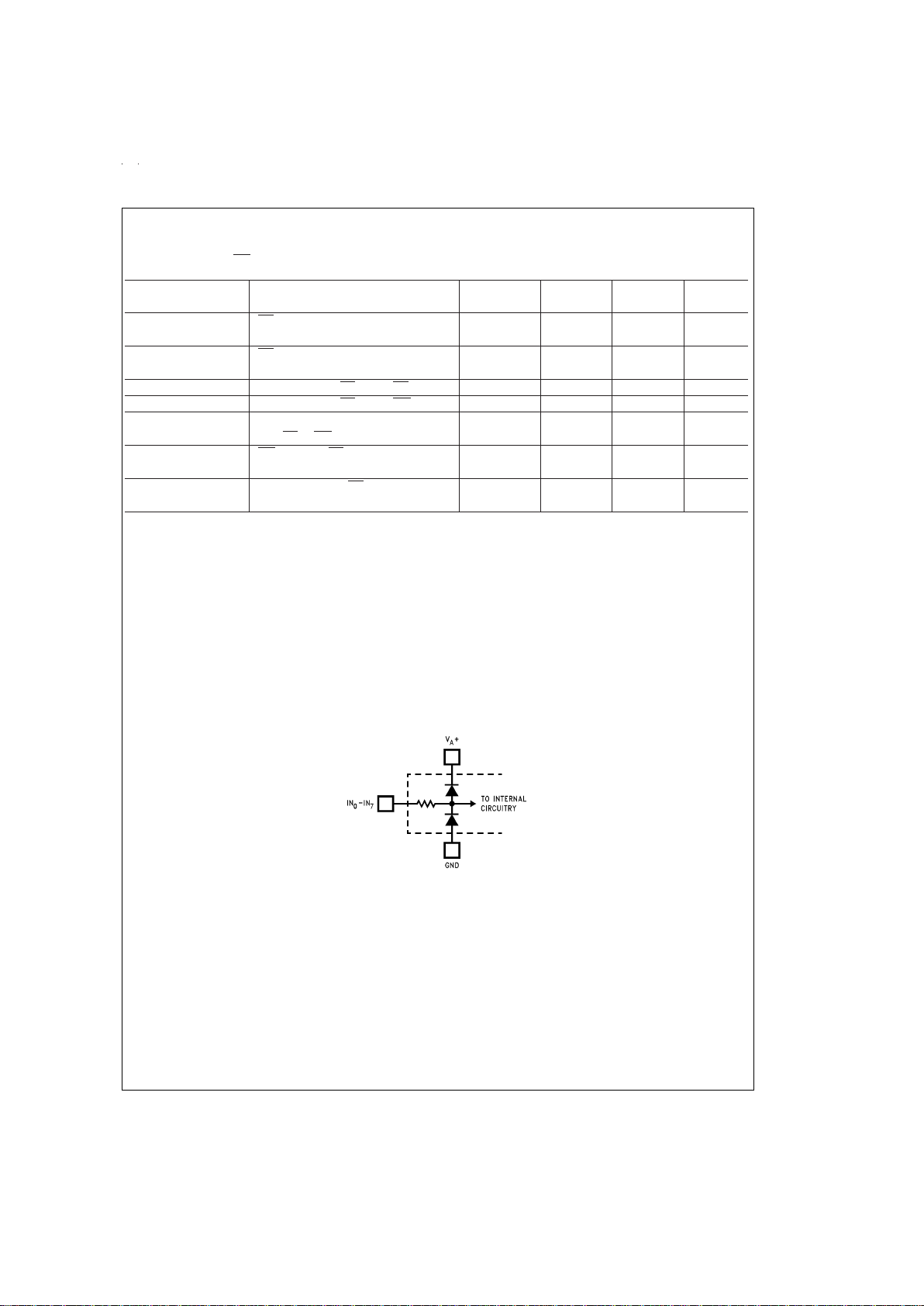
Note 6: Two on-chip diodes are tied to each analog input through a series resistor, as shown below. Input voltage magnitude up to 5V above V
A
+ or 5V below GND
will not damage the LM12454 or the LM12(H)458. However, errors in the A/D conversion can occur if these diodes are forward biased by more than 100 mV.As an
example, if V
A
+ is 4.5 VDC, full-scale input voltage must be ≤4.6 VDCto ensure accurate conversions.
Note 7: V
A
+ and VD+ must be connected together to the same power supply voltage and bypassed with separate capacitors at each V+pin to assure conversion/
comparison accuracy.
Note 8: Accuracy is guaranteed when operating at f
CLK
=
5 MHz for the LM12454/8 and f
CLK
=
8 MHz for the LM12H458.
Note 9: With the test condition for V
REF(VREF+−VREF−
) given as +5V, the 12-bit LSB is 1.22 mV and the 8-bit/“Watchdog” LSB is 19.53 mV.
Note 10: Typicals are at T
A
=
25˚C and represent most likely parametric norm.
Note 11: Limits are guaranteed to National’s AOQL (Average Output Quality Level).
Note 12: Positive integral linearity error is defined as the deviation of the analog value, expressed in LSBs, from the straight line that passes through positive
full-scale and zero. For negative integral linearity error the straight line passes through negative full-scale and zero. (See
Figure 6 Figure 7
).
Note 13: Zero error is a measure of the deviation from the mid-scale voltage (a code of zero), expressed in LSB. It is the worst-case value of the code transitions
between −1 to 0 and 0 to +1 (see
Figure 8
).
Note 14: The DC common-mode error is measured with both inputs shorted together and driven from 0V to 5V.The measured value is referred to the resulting output value when the inputs are driven with a 2.5V signal.
Note 15: Power Supply Sensitivity is measured after Auto-Zero and/or Auto-Calibration cycle has been completed with V
A
+ and VD+ at the specified extremes.
Note 16: V
REFCM
(Reference Voltage Common Mode Range) is defined as (V
REF++VREF−
)/2.
DS011264-3
www.national.com9
Digital Timing Characteristics (Notes 6, 7, 8, 19) (Continued)
Note 17: The LM12(H)454/8’s self-calibration technique ensures linearity and offset errors as specified, but noise inherent in the self-calibration process will result
in a repeatability uncertainty of
±
0.10 LSB.
Note 18: The Throughput Rate is for a single instruction repeated continuously. Sequencer states 0 (1 clock cycle), 1 (1 clock cycle), 7 (9 clock cycles) and 5 (44
clock cycles) are used (see
Figure 15
). One additional clock cycle is used to read the conversion result stored in the FIFO, for a total of 56 clock cycles per con-
version. The Throughput Rate is f
CLK
(MHz)/N, where N is the number of clock cycles/conversion.
Note 19: A military RETS specification is available upon request.
Electrical Characteristics
DS011264-22
V
REF
=
V
REF+−VREF−
V
IN
=
V
IN+−VIN−
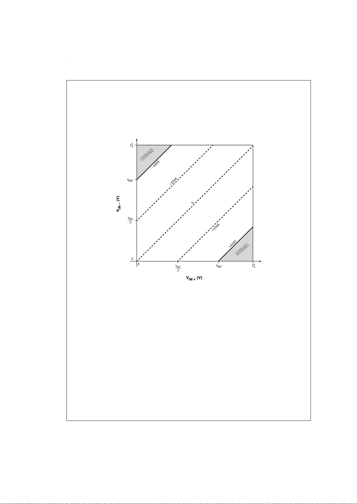
GND ≤ V
IN+≤VA
+
GND ≤ V
IN−≤VA
+
FIGURE 1. The General Case of Output Digital Code vs the Operating Input Voltage Range
www.national.com 10
Electrical Characteristics (Continued)
DS011264-23
V
REF+−VREF−
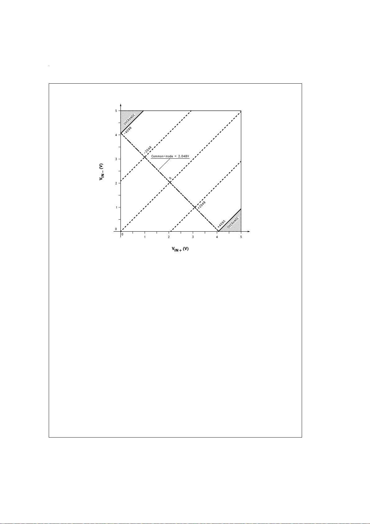
=
4.096V
V
IN
=
V
IN+−VIN−
GND ≤ V
IN+≤VA
+
GND ≤ V
IN−≤VA
+
FIGURE 2. Specific Case of Output Digital Code vs the Operating Input Voltage Range for V
REF
=
4.096V
www.national.com11
Electrical Characteristics (Continued)
DS011264-24
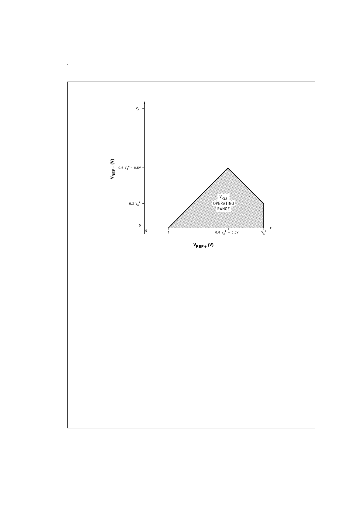
V
REF
=
V
REF+−VREF−
FIGURE 3. The General Case of the V
REF
Operating Range
www.national.com 12
Electrical Characteristics (Continued)
DS011264-25
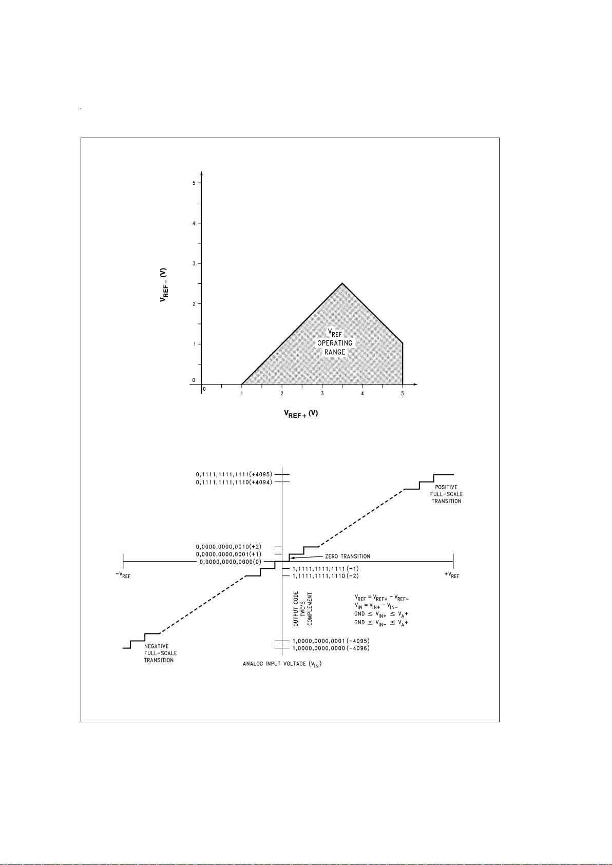
V
REF
=
V
REF+−VREF−
VA+=5V
FIGURE 4. The Specific Case of the V
REF
Operating Range for VA+=5V
DS011264-4
FIGURE 5. Transfer Characteristic
www.national.com13
 Loading...