NSC LM1283N Datasheet

April 1999
LM1283
140 MHz RGB Video Amplifier System with On Screen
Display (OSD)
General Description
The LM1283 is a full feature video amplifier with OSD inputs,
all within a 28-pin package. This part is intended for use in
monitors with resolutions up to 1280 x 1024. The video section of the LM1283 features three matched video amplifiers
with blanking. All of the video amplifier adjustments feature
high input impedance 0V to 4V DC controls, providing easy
interfacing to bus controlled alignment systems. The OSD
section features three TTL inputs and a DC contrast control.
The switching between the OSD and video section is controlled by a single TTL input. Although the OSD signals are
TTL inputs, these signals are internally processed to match
the OSD logic low level to the video black level. When adjusting the drive controls for color balance of the video signal, the color balance of the OSD display will track these
color adjustments. The LM1283 also features an internal
spot killer circuit to protect the CRT when the monitor is
turned off. For applications without OSD insertion please refer to the LM1205 or LM1208 data sheets.
Features
n Three wideband video amplifiers 140 MHz@−3 dB
(4 V
output)
PP
n TTL OSD inputs, 50 MHz bandwidth
n On chip blanking, outputs under 0.1 V when blanked
n Video/OSD switch speed of 7 ns
n Independent drive control for each channel for color
balance
n 0V to 4V, high impedance DC contrast control with over
40 dB range
n 0V to 4V, high impedance DC drive control (0 dB to
−12 dB range)
n 0V to 4V, high impedance DC OSD contrast control with
over 40 dB range
n Capable of 6.5 V
bandwidth)
n Output stage directly drives most hybrid or discrete CRT
drivers
output swing (slight reduction in
PP
Applications
n High resolution RGB CRT monitors requiring OSD
capability
LM1283 140 MHz RGB Video Amplifier System with On Screen Display (OSD)
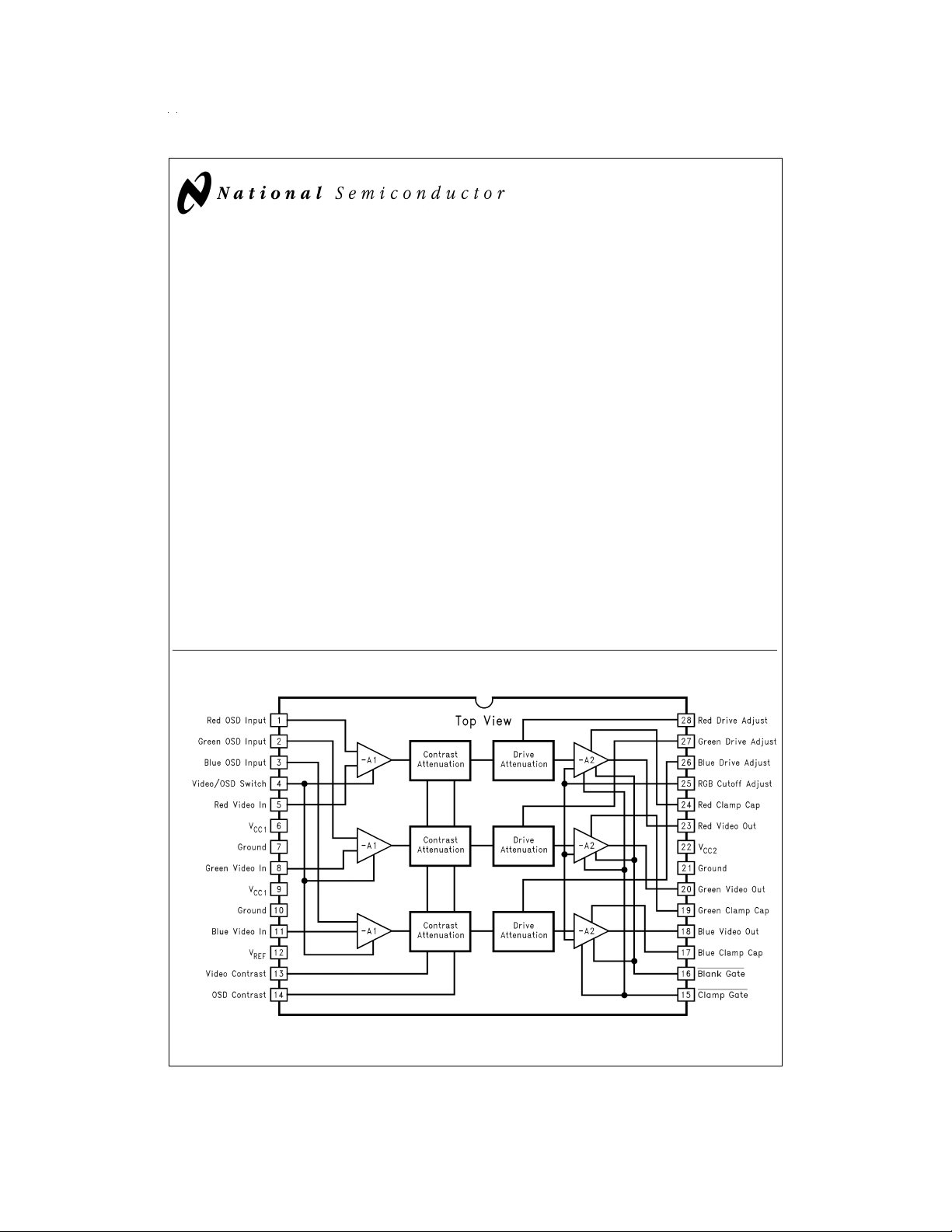
Block and Connection Diagram
DS012684-1
FIGURE 1. Order Number LM1283N
See NS Package Number N28B
© 1999 National Semiconductor Corporation DS012684 www.national.com

Absolute Maximum Ratings (Note 1)
If Military/Aerospace specified devices are required,
please contact the National Semiconductor Sales Office/
Distributors for availability and specifications.
Supply Voltage
Pins 6, 9, and 22 15V
Peak Video Output Source Current
(Any One Amp) Pins 18, 20, and 23 28 mA
Voltage at Any Input Pin (V
Power Dissipation (P
(Above 25˚C Derate based on θ
and TJ) 2.5W
Thermal Resistance to Ambient (θ
)V
IN
)
D
JA
) 45˚C/W
JA
≥ VIN≥ GND
CC
Thermal Resistance to Case (θ
Junction Temperature (T
) 28˚C/W
JC
) 150˚C
J
ESD Susceptibility (Note 4) 2 kV
ESD Machine Model (Note 17) 200V
Storage Temperature −65˚C to +150˚C
Lead Temperature
(Soldering, 10 sec.) 265˚C
Operating Ratings (Note 2)
Temperature Range −20˚C to +70˚C
Supply Voltage (V
) 11.4V ≤ VCC≤ 12.6V
CC
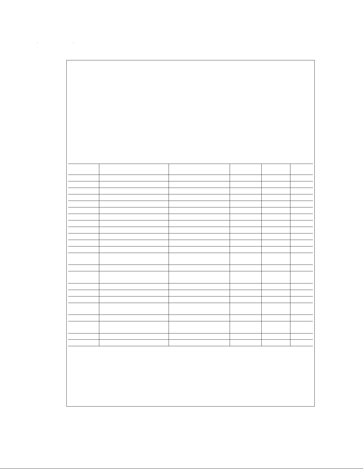
DC Electrical Characteristics
See DC Test Circuit (
=
0V; V
1V unless otherwise stated
25
Figure 5
), T
A
=
25˚C; V
Symbol Parameter Conditions
I
S
R
IN
V
15l
V
15h
I
15l
I
15h
V
16l
V
16h
I
16l
I
16h
V
12
I
vid-clamp
I
vid-bias
I
out-clamp
I
out-bias
V
OL
V
OH
V
O(1V)
∆V
O(1V)
(blanked) Video Output Blanked Voltage Blank Gate On (V16≤ 0.8V) 100 500 mV (max)
V
OL
I
13, 14, 26, 27, or
28
I
25
V
spot
Supply Current V
Video Input Resistance Any One Amplifier 100 kΩ
Clamp Gate Low Input Voltage Clamp Comparators On 1.2 0.8 V (max)
Clamp Gate High Input Voltage Clamp Comparators Off 1.6 2.0 V (min)
Clamp Gate Low Input Current V
Clamp Gate High Input Current V
Blank Gate Low Input Voltage Blank Gate On 1.2 0.8 V (max)
Blank Gate High Input Voltage Blank Gate Off 1.6 2.0 V (min)
Blank Gate Low Input Current V
Blank Gate High Input Current V
Reference Voltage 2.0 V
Video Input Cap Charge Current Clamp Comparators On
Video Input Cap Bias Discharge
Current
Output Clamp Charge Current Clamp Comparators On
Output Clamp Bias Discharge
Current
Video Output Low Voltage V
Video Output High Voltage V
Video Black Level Output Voltage V
Video ∆Black Level Output
Voltage
Contrast/Drive Control Input
Current
Cut-Off Control Input Current V
Spot Killer Voltage VCCAdjusted to Activate 10.6 11.2 V (max)
=
=
V
CC1
12V; V
CC2
CC1+VCC2,RL
=
0V −8.0 µA (max)
15
=
12V 0.01 1.0 µA (max)
15
=
0V −4.0 µA (max)
16
=
12V 0.01 1.0 µA (max)
16
Clamp Comparators Off
Clamp Comparators Off
=
0V 50 100 mV (max)
25
=
10V 8.2 7.5 V (min)
25
=
1V 1.0 V (Note 8)
25
Between Any Two Amplifiers,
=
1V
V
25
=
V
contrast
=
0V to 4V −0.25 −2.0 µA (max)
25
=
13
=
=
4V; V
14
∞
f (Note 7) 85 130 mA (max)
4V; V
=
4V; V
16
Typical
(Note 5)
±
900
±
450 nA
±
850
drive
=
4V; V
Limit
(Note 6)
±
±
150 nA
±
20
=
V
0V to 4V
drive
−125 −500 nA (max)
±
=
0V; V
4
400 µA (min)
450 µA (min)
250 mV (max)
15
Units
=
www.national.com 2

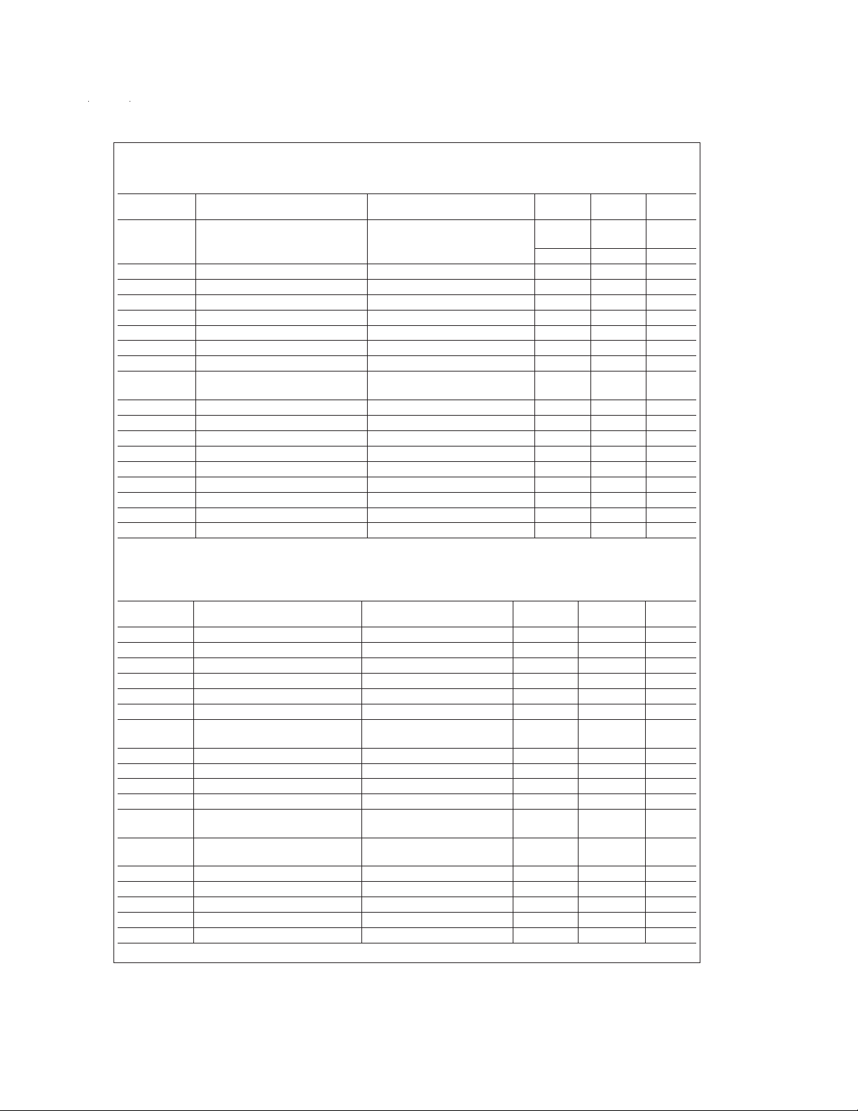
AC Electrical Characteristics
See AC Test Circuit (
4V DC for the AC test unless otherwise stated (Note 15)
Figure 6
), T
A
=
25˚C, V
Symbol Parameter Conditions
A
V max
∆A
V2V
∆A
V 0.25V
∆Drive
∆Drive
A
V match
A
V track
2V
0.25V
Video Amplifier Gain V
Contrast Attenuation@2V Ref: AVmax, V
Contrast Attenuation@0.25V Ref: AVmax, V
Drive Attenuation@2V Ref: AVmax, V
Drive Attenuation@0.25V Ref: AVmax, V
Absolute Gain Match@AVmax V
Gain Change between Amplifiers V
THD Video Amplifier Distortion V
f(−3 dB) Video Amplifier Bandwidth
(Notes 11, 12)
(Video) Video Output Rise Time (Note 11) V
t
r
t
(Video) Video Output Fall Time (Note 11) V
f
V
10 kHz Video Amplifier 10 kHz Isolation V
sep
V
10 MHz Video Amplifier 10 MHz Isolation V
sep
t
(Blank) Blank Output Rise Time (Note 11) Blank Output=1V
r
t
(Blank) Blank Output Fall Time (Note 11) Blank Output=1V
f
t
(Blank) End of Blanking Propagation Delay Blank Output=1V
r-prop
t
(Blank) Start of Blanking Propagation Delay Blank Output=1V
f-prop
T
(Clamp) Back Porch Clamp Pulse Width (Note 14) 200 ns (min)
pw
CC1
=
=
V
CC2
13
V
drive
13
13
O
V
13
V
O
O
O
13
13
=
12V; V
=
=
=
=
=
=
=
=
=
=
0V. Manually adjust Video Output pins 18, 20, and 23 to
4
Typical
(Note 5)
=
4V, V
=
4V, V
4V to 2V (Notes 9, 10)
1V
4V, V
4V
4V
4V
400 mV
IN
PP
10.0 7.0
4V 20.0 16.9 dB (min)
=
2V −6 dB
13
=
0.25V −24 dB
13
=
2V −4.5 dB
drive
=
0.25V −10 dB
drive
=
4V (Note 9)
drive
,f=10 kHz 1
PP
=
3V,
drive
PP
PP
PP
±
0.2 dB
±
0.2 dB
140 MHz
2.3 ns
3.3 ns
Limit
(Note 6)
4V (Note 13) −70 dB
4V (Notes 11, 13) −50 dB
PP
PP
PP
PP
8ns
14 ns
23 ns
20 ns
Units
V/V
(min)
%
OSD Electrical Characteristics
See DC Test Circuit (
=
0V; V
1V unless otherwise stated
25
Figure 5
), T
A
=
25˚C; V
Symbol Parameter Conditions
V
OSDI
V
OSDh
V
4l
V
4h
I
4l
I
4h
∆V
O-OSD(1V)
V
OSD-out
∆V
OSD-out
∆V
OSD-out match
V
OSD-out track
t
(OSD S) Video to OSD Switch Time (Note
r
(OSD S) OSD to Video Switch Time (Note
t
f
(OSD S) Video to OSD Propagation Delay V
t
r-prop
t
(OSD S) OSD to Video Propagation Delay V
f-prop
t
(OSD) OSD Rise Time at VO(Note 11) V
r
t
(OSD) OSD Fall Time at VO(Note 11) V
f
t
(OSD) Starting OSD Propagation Delay V
r-prop
OSD Input Low Input Voltage 1.2 0.4 V (max)
OSD Input High Input Voltage 1.6 2.0 V (min)
OSD Select Low Input Voltage Video Inputs are Selected 1.2 0.8 V (max)
OSD Select High Input Voltage OSD Inputs are Selected 1.6 2.0 V (min)
OSD Select Low Input Current V
OSD Select High Input Current V
OSD ∆Black Level Output Voltage,
Difference from Video Output
OSD Output Voltage V
PP
OSD Output VPPAttenuation V
Output Match between Channels V
Output Variation between Channels V
11)
11)
CC1
=
=
V
12V; V
CC2
4
4
V
25
V
14
14
14
14
V
1
V
1
1
1
14
14
14
13
=
0V −3.0 −6.0 µA (max)
=
12V 0.001 1.0 µA (min)
=
1V
=
4V, V
=
2V, V
=
4V, V
=
4V to 2V, V
=
=
V
V
2
=
=
V
V
2
=
=
V
V
2
=
=
V
V
2
=
4V; V
=
4V; V
=
4V; V
Drive
Drive
Drive
3
3
3
3
25
25
25
=
=
=
=
=
=
=
=
=
4V; V
14
=
2V 5.0 V
=
2V 50 30
=
2V
=
2V
Drive
4V (Note 16)
4V (Note 16)
=
V
V
13
14
=
V
V
13
14
4V; V
16
=
4V; V
Typical
(Note 5)
=
Drive
±
150 mV
±
2.0
±
2.0
4V; V
Limit
(Note 6)
=
4
4ns
11 ns
=
4V 11 ns
=
4V 12 ns
1V 4 ns
1V 10 ns
1V 6.5 ns
4V; V
www.national.com3
15
%
=
Units
PP
(min)
%
%

OSD Electrical Characteristics (Continued)
See DC Test Circuit (
=
0V; V
1V unless otherwise stated
25
Figure 5
), T
A
=
25˚C; V
Symbol Parameter Conditions
(OSD) Ending OSD Propagation Delay V
t
f-prop
V
10 kHz Video Feedthrough into OSD V
feed
V
10 MHz Video Feedthrough into OSD V
feed
Note 1: Absolute Maximum Rating indicate limits beyond which damage to the device may occur.
Note 2: Operating Ratings indicate conditions for which the device is functional, but do not guarantee specific performance limits. For guaranteed specifications and
test conditions, see the Electrical Characteristics. The guaranteed specifications apply only for the test conditions listed. Some performance characteristics may degrade when the device is not operated under the listed test conditions.
Note 3: V
Note 4: Human body model, 100 pF discharged through a 1.5 kΩ resistor.
Note 5: Typical specifications are specified at +25˚C and represent the most likely parametric norm.
Note 6: Tested limits are guaranteed to National’s AOQL (Average Outgoing Quality Level).
Note 7: The supply current specified is the quiescent current for V
depends on the output load. With video output at 1V DC, the additional current through V
Note 8: Output voltage is dependent on load resistor. Test circuit uses R
Note 9: Measure gain difference between any two amplifiers. V
Note 10: ∆A
gain change between any two amplifiers with the contrast voltage (V
max the three amplifiers’ gains might be 17.1 dB, 16.9 dB, and 16.8 dB and change to 11.2 dB, 10.9 dB and 10.7 dB respectively for V
sured typical
Note 11: When measuring video amplifier bandwidth or pulse rise and fall times, a double sided full ground plane printed circuit board without socket is recommended. Video amplifier 10 MHz isolation test also requires this printed circuit board. The reason for a double sided full ground plane PCB is that large measurement
variations occur in single sided PCBs.
Note 12: Adjust input frequency from 10 MHz (A
Note 13: Measure output levels of the other two undriven amplifiers relative to the driven amplifier to determine channel separation. Terminate the undriven amplifier
inputs to simulate generator loading. Repeat test at f
Note 14: A minimum pulse width of 200 ns is guaranteed for a horizontal line of 15 kHz. This limit is guaranteed by design. If a lower line rate is used a longer clamp
pulse may be required.
Note 15: During the AC test the 4V DC level is the center voltage of the AC output signal. For example, if the output is 4 V
and 6V DC.
Note 16: When V
shown in
Note 17: Machine Model ESD test is covered by specification EIAJ IC-121-1981. A 200 pF cap is charged to the specified voltage, then discharged directly into the
IC with no external series resistor (resistor of discharge path must be under 50Ω).
supply pins 6, 9, and 22 must be externally wired together to prevent internal damage during VCCpower on/off cycles.
CC
track is a measure of the ability of any two amplifiers to track each other and quantifies the matching of the three attenuators. It is the difference in
V
±
0.1 dB channel tracking.
V
=
=
=
V
V
1
Figure 3
. Thus tr(OSD) is actually a fall time and tf(OSD) is actually a rise time in this condition.
0V and the video input is 0.7V,then t
2
3
=
=
V
CC1
max reference level) to the −3 dB corner frequency (f
=
10 MHz for V
IN
12V; V
CC2
=
14
=
14
=
V
1
=
14
=
V
1
and V
CC1
=
L
=
635 mV
IN
) at either 4V or 2V measured relative to an AVmax condition, V
13
sep 10 MHz
(OSD)=11ns and tf(OSD)=4 ns. The Video Output waveform will be inverted from the one
r
4V; V
4V; V
V
2
4V; V
V
2
CC2
390Ω.
.
PP
=
=
with R
.
=
13
=
25
=
25
=
V
3
=
25
=
V
3
L
=
4V; V
14
1V 9 ns
1V;
0V
1V;
0V
=
∞
, see
Figure
is 8 mA for
CC2
4V; V
16
=
4V; V
Typical
(Note 5)
Drive
=
4V; V
(Note 6)
−70 dB
−60 dB
5’s test circuit. The supply current for V
Figure 5
’s test circuit.
13
=
13
).
−3 dB
the signal will swing between 2V DC
PP
=
4V; V
4
15
Limit
(pin 22) also
CC2
=
4V. For example, at A
2V.This yields the mea-
=
Units
V
www.national.com 4
 Loading...