


LM1253A
Monolithic Triple 180 MHz I
2
C CRT Pre-amp With
Integrated Analog On Screen Display (OSD) Generator
General Description
The LM1253A pre-amp is an integrated high voltage triple
CRT pre-amp and Analog On Screen Display (OSD) generator. The IC is I
2
C controlled, and allows control of all the parameters necessary to setup and adjust the brightness and
contrast in the CRT display. In addition, it provides a programmable period vertical blanking pulse which is used to
blank the G1.
The LM1253A pre-amp is designed to work in cooperation
with the LM2453 driver, and provides a multiplexed video
signal (VideoPlex) interface to enable the DC clamp levels at
the cathode to be varied in order to set up the CRT bias and
to allow individual adjustment for brightness.
TheAnalogOSDhas a selectable palette allowing a wide selection of colors. The preset level of the OSD can be controlled by I
2
C to suit different CRT displays. The OSD signal
is internally mixed with the video signal, before the gain section, and thus gives excellent white tracking of the OSD with
the white color point setting of the video.
The Brightness settings are also mixed into the video signal
before the gain matching controls and consequently give excellent white color point tracking with variations in the Brightness control. An active horizontal blanking signal is added to
the video at the output, giving excellent smear performance,
and preventing video content dependent DC bias offsets as
a result of high frequency over shoot.
The OSD horizontal sync and blanking signal is derived from
a positive going flyback pulse. The digital section provides
easy interfacing of this signal with the deflection circuits.
The vertical blanking signal is taken from the vertical sync
signal, and the blanking duration is programmable. This system is highly integrated and requires a minimal number of
external components.
Black level clamping of the signal is carried out directly on
the AC coupled input signal into the high impedance preamplifier input, thus eliminating the need for additional black
level clamp capacitors.
The outputs are referenced to a DC level produced by the
LM1253A Pre-amp, and so are guaranteed to provide stable
DC operating levels within the system without the need for
additional external feedback components.
The IC is packaged in an industry standard wide body 28lead DIL molded plastic package.
Features
n 190 two-color ROM based Character Fonts
n 64 four-color ROM based Character Fonts
n Supports a programmable page size with up to 512
characters and line definition codes
n Support for 2 Display Windows (size of each window is
configurable)
n Programmable start position for each Display Window
n Programmable Resolutions: from 512 to 960 pixels per
line in 64 pixel increments
n Programmable Character Height, with automatic height
control with mode change
n Programmable Row Spacing between each display
character row
n Maximum Pixel clock of 92.2 MHz
n I
2
C compatible interface to controlling micro-controller
n Button boxes
n 180 MHz preamplifier with full video signal parametric
control
n VideoPlex
™
interface to the LM2453 driver
n OSD mixing with 64 out of 512 color mask
programmable selection
Intended Applications
n 1280 x 1024 Displays up to 75 Hz requiring OSD
capability
May 2000
LM1253A Monolithic Triple 180 MHz I
2
C CRT Pre-amp With Integrated Analog On Screen Display
(OSD) Generator
© 2000 National Semiconductor Corporation DS101265 www.national.com

Table of Contents
Block and Connection Diagrams 3
Absolute Maximum Ratings 5
Operating Ratings 5
Electrical Characteristics 5
Test Circuit 7
Test Settings 8
Pin Descriptions 8
Input/Output Schematics 13
National VideoPlex Video System 15
ESD and Arc-Over Protection 16
Pre-Amp Functional Description 17
Horizontal Phase Locked Loop 19
Fault Operation 19
Power Save Mode 19
Schematics 20
PCB Layout 22
OSD Generator Operation 23
Micro-Controller Interface 27
LM1253A Address Map 29
Pre-Amp Interface Registers 30
Two-Color Attribute Table 31
Four-Color Attribute Table 31
Display Page RAM 32
Controller Register Definitions 40
Character Font 51
List of Tables
Table 1 Control Test Settings 7
Table 2 Registers Controlling the Output
Video and Clamp Signal 18
Table 3 Character ROM Address Map 29
Table 4 Display Page RAM Address Map 29
Table 5 OSD Interface Registers 30
Table 6 Pre-Amp Interface Registers 31
Table 7 Two-Color Attribute Registers 31
Table 8 Four-Color Attribute Registers 31
Table 9 Example 1 I
2
C Transmission 35
Table 10 Example 2 I
2
C Transmissions 36
Table 11 Example 3 I
2
C Transmissions 39
Table 12 PLL Setting (Register 843Eh) 46
Table 13 Attribute Tables to I
2
C Address 48
LM1253A
www.national.com 2
Block and Connection Diagrams
DS101265-1
FIGURE 1. Block Diagram
LM1253A
www.national.com3
Block and Connection Diagrams (Continued)
28-Lead (0.600’’ wide) Molded Dual-In-Line Package
DS101265-2
Order Number LM1253AN
See NS Package Number N28B
FIGURE 2. Connection Diagram
LM1253A
www.national.com 4

Absolute Maximum Ratings (Notes 1, 3)
If Military/Aerospace specified devices are required,
please contact the National Semiconductor Sales Office/
Distributors for availability and specifications.
Supply Voltage, (V
CC
)6V
Input Voltage, (V
IN
)6V
Storage Temperature Range, (T
STG
) −65˚C to +150˚C
T
JMAX
150˚C
Lead Temperature (Soldering,
<
10 sec.) 300˚C
ESD Tolerance, Human Body Model 3 kV
Machine Model 300V
Operating Ranges (Note 2)
Temperature Range 0˚C to +70˚C
V
CC
+4.75V to +5.25V
Active Video Signal Electrical Characteristics
(See
Figure 3
for Test Circuit, and
Table 1
for Control Test Settings Chart)
Unless otherwise noted: V
CC
= +5V, VIN= 0.7V, CL= 8 pF, Video Signal Output = 1 VPP,TA= 25˚C, V
ABL=VCC
.
Symbol Parameter Conditions
LM1253A
Units
Min Typ Max
I
CC1MAX
Maximum Supply Current Test Setting 1, No Output Load 245 mA
V
OUT BLK
Active Video Black Level Minimum
Output Voltage
Test Setting 1, No AC Input Signal
V
REF
V
DC
LE Linearity Error Test Setting 3, (Note 4), Triangular
Step Signal Input
1%
V
OUT WHITE
Active Video White Level Max
Output Voltage
Test Setting 3, AC Input Signal
2.7 V
t
r
Rise Time Test Setting 3, (Note 5), 10% to
90%, AC Input Signal
3.0 ns
t
f
Fall Time Test Setting 3, (Note 5), 90% to
10%, AC Input Signal
3.0 ns
OS
R
Rising Edge Overshoot Test Setting 3, (Note 5), AC Input
Signal
5%
OS
F
Falling Edge Overshoot Test Setting 3, (Note 5), AC Input
Signal
5%
f(−3dB) Video Amplifier Bandwidth Measured in AC2DC002 Demo
Board. LM1253A set for 40 V
PP
swing at LM2453 output
180 MHz
A
CONTRAST
Contrast Max-Min Adjustment
Range
Test Setting 2, AC Input Signal
20 dB
A
GAIN
Gain Max-Min Adjustment Range Test Setting 2, AC Input Signal 10 dB
A
MAX
Max Signal Voltage Gain Test Setting 2, AC Input Signal 1.8 V/V
V
ABL TH
Auto Beam Limit Control Upper
Limit
Test Setting 3, (Note 6), AC Input
Signal
4.5 V
V
ABL RANGE
Auto Beam Limit Control Voltage
Range
Test Setting 3, (Note 6), AC Input
Signal
3V
∆A
ABL
Auto Beam Limit Control Range Test Setting 3, (Note 6), AC Input
Signal
−10 dB
I
ABL MAX
Auto Beam Limit Input Current
Sink Capability
Test Setting 3, (Note 6), AC Input
Signal
1mA
C
IP
Input AC Coupling Capacitor Test Setting 3 4.7 nF
V
REF
Typical V
REF
Output Voltage 1.55 1.65 1.75 V
XT Channel to Channel Crosstalk 10 MHz 40 dB
LM1253A
www.national.com5
Brightness/Bias Signal Electrical Characteristics
(See
Figure 3
for Test Circuit, and
Table 1
for Control Test Settings Chart)
Unless otherwise noted: VCC= +5V, VIN= 0.7V, CL= 8 pF, Video Signal Output = 1 VPP,TA= 25˚C, V
ABL=VCC
.
Symbol Parameter Conditions
LM1253A
Units
Min Typ Max
V
BLANK MAX
Maximum Blanking Level Test Setting 1 V
REF
−
0.90
V
V
BLANK MIN
Minimum Blanking Level Test Setting 4 V
REF
V
t
BLK r
Blanking Rise Time Test Setting 1, 10% to 90%, 10 ns
t
BLK f
Blanking Fall Time Test Setting 1, 90% to 10%, 10 ns
OS
BLK MAX
Maximum Rise or Fall Edge
Overshoot
Test Setting 1, 10% to 90% or
90% to 10%, Settling Time Must
be Less Than 50 ns
20 %
OSD Electrical Characteristics
(See
Figure 3
for Test Circuit)
Unless otherwise noted: VCC= +5V, VIN= 0.7V, CL= 8 pF, Video Signal Output = 1 VPP,TA= 25˚C, V
ABL=VCC
.
Symbol Parameter Conditions
LM1253A
Units
Min Typ Max
V
OSDHIGH MAX
Maximum OSD Level with OSD
Contrast 11
Palette Set at 111. OSD Contrast
Level 11, Test Setting 3
V
REF
+
0.95
V
V
OSDHIGH 10
Maximum OSD Level with OSD
Contrast 10
Palette Set at 111. OSD Contrast
Level 10, Test Setting 3
V
REF
+
0.77
V
V
OSDHIGH 01
Maximum OSD Level with OSD
Contrast 01
Palette Set at 111. OSD Contrast
Level 01, Test Setting 3
V
REF
+
0.59
V
V
OSDHIGH 00
Maximum OSD Level with OSD
Contrast 00
Palette Set at 111. OSD Contrast
Level 00, Test Setting 3
V
REF
+
0.41
V
External Interface Signals Electrical Characteristics
(See
Figure 3
for Test Circuit)
Unless otherwise noted: VCC= +5V, VIN= 0.7V, CL= 8 pF, Video Signal Output = 1 VPP,TA= 25˚C, V
ABL=VCC
.
Symbol Parameter Conditions
LM1253A
Units
Min Typ Max
I
IN−MAX
Maximum normal forward scan current at
lowest horizontal frequency that input can
withstand
−150 µA
V
HBLANK TRIG
Voltage on H Flyback (Pin 14) which will
Trigger an HBLANK Signal
100V H Flyback Signal
through a 100 kΩ
Resistor
0.8 V
I
IN+MAX
Maximum flyback scan current at 125 kHz
that input can withstand
1.5 mA
t
min hflb
Minimum Flyback Width 1 µs
t
H
Horizontal Period 20 125 kHz
t
PW CLAMP
Minimum Clamp Pulse Width 200 ns
V
CLAMP L MAX
Maximum Low Level Clamp Pulse Voltage 1 V
V
CLAMP H MIN
Minimum High Level Clamp Pulse Voltage 3 V
V
VBLANK HIGH
Minimum High Level of Vertical Blank
Output
V
VREF BLANK
<
0.75V V
REF
+1
V
V
VBLANK LOW
Maximum Low Level of Vertical Blank
Output
I
VBLANK OUT
= 100 µA V
REF
−1
V
LM1253A
www.national.com 6
External Interface Signals Electrical Characteristics (Continued)
(See
Figure 3
for Test Circuit)
Unless otherwise noted: VCC= +5V, VIN= 0.7V, CL= 8 pF, Video Signal Output = 1 VPP,TA= 25˚C, V
ABL=VCC
.
Symbol Parameter Conditions
LM1253A
Units
Min Typ Max
V
CCDET
VCCUndervoltage Detection Threshold 3.9 V
F
FREE_RUN
Free Run HBLANK Frequency 30 60 kHz
V
IL
Low Level Input Voltage for SDA and SCL
Pins
1.5 V
V
IH
High Level Input Voltage for SDA and SCL
Pins
3V
V
OL
Low Level Output Voltage for SDA and SCL
Pins
3 mA Sink Current
0 0.4 V
Note 1: Absolute Maximum Ratings indicate limits beyond which damage to the device may occur.
Note 2: Operating Ranges indicate conditions forwhichthedevice is functional, but do not guarantee specific performance limits. For guaranteed specifications and
test conditions, see the Electrical Characteristics. The guaranteed specifications apply only for the test conditions listed. Some performance characteristics may
change when the device is not operated under the listed test conditions.
Note 3: All voltages are measured with respect to GND, unless otherwise specified.
Note 4: Linearity Error = 100
*
(step
max
–step
min
)/step
ave
Where: The input signal is a 16 step staircase signal waveform with 0.7 V
P-P
level, subdivided into 16 equal steps, with each step approximately 100 ns in width
step
max
is the maximum voltage step at the output
step
min
is the minimum voltage step at the output
step
ave
is the average voltage of the 16 steps at the output.
Note 5: Input from signal generator: t
r,tf
<
1 ns.
Note 6: ABL should provide smooth decrease in gain over the operational range of 0 dB to −5 dB
∆A
ABL
= A(V
ABL=VABL MAX GAIN
)–A (V
ABL=VABL MIN GAIN
)
Test Circuit
DS101265-3
Note: 8 pF load includes parasitic capacitance
FIGURE 3. Test Circuit
LM1253A
www.national.com7
Test Settings
TABLE 1. Control Test Settings
Control
No.
of
Bits
Basic
Test
Setting 1
Basic
Test
Setting 2
Basic
Test
Setting 3
Basic
Test
Setting 4
Contrast 7 Max
(Hex 7F)
Max
(Hex 7F)
Max
(Hex 7F)
Max
(Hex 7F)
R,G,B Gain 7 Max
(Hex 7F)
Max
(Hex 7F)
Set for 1 V
P-P
on all Channels
Max
(Hex 7F)
Brightness 8 Max
(Hex FF)
Max
(Hex FF)
Min
(Hex 00)
Min
(Hex 00)
R,G,B Bias 8 Max
(Hex FF)
Max
(Hex FF)
Min
(Hex 00)
Min
(Hex 00)
DC Offset 3 Min
(Hex 07)
Max
(Hex 00)
Min
(Hex 07)
Min
(Hex 07)
Pedestal Offset 3 Max
(Hex 07)
Max
(Hex 07)
Min
(Hex 00)
Min
(Hex 00)
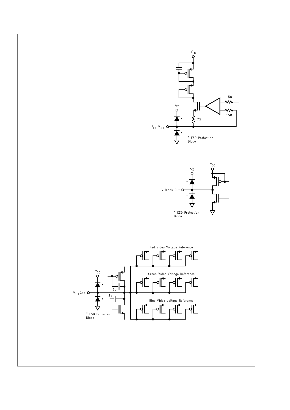
Pin Descriptions
Pin 1 —R
EXTVREF
A10kΩ1% resistor is connected to this
pin to set up the internal current sources. The LM1253A is
optimized for this value of resistor. A DC voltage only will be
on this pin. Decreasing the value of this resistor will increase
supply current while degrading performance; increasing the
value of the resistor will decrease supply current and also
degrade the performance. Do not place the resistor close to
sources of heat such as the CRT driver.
Figure 29
shows the
components connected to pin 1,
Figure 11
shows the internal
schematic of pin 1.
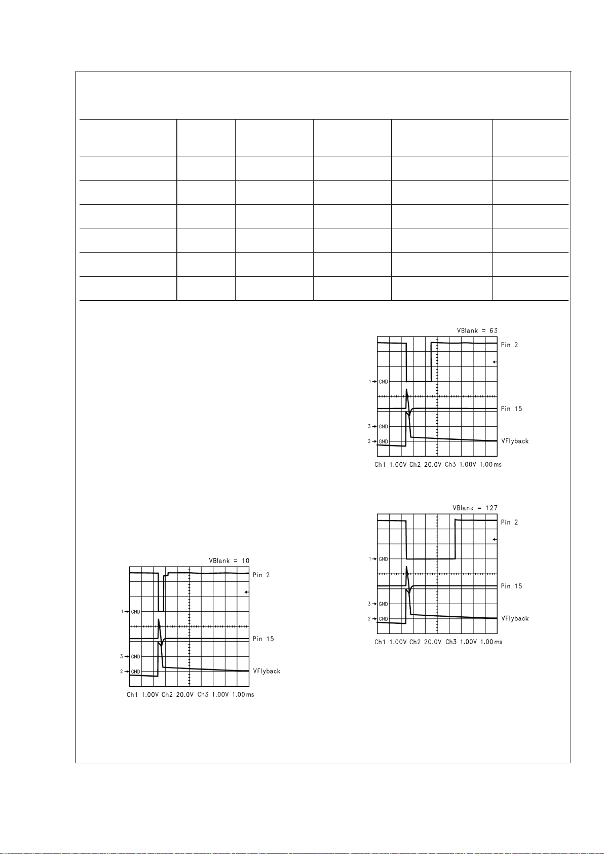
Pin 2—V Blank Out This pin supplies a variable width,
negative going pulse at the vertical rate to the CRT Driver. V
Blank is triggered from the signal on pin 15, which comes
from the vertical flyback. The CRT Driver supplies the pull up
for this pin. The width of this pulse is set by the value in the
VBLANKDUR register (8403h).
Figures 4, 5, 6
show the resulting V Blank Out pulse with various values in register
8403h. The trace connecting pin 2 of the LM1253A to the
LM2453 must be kept away from the output circuitry of the
LM2453.
Figure 29
shows the external schematic of pin 2,
Figure 12
shows the internal schematic of pin 2.
Pin 3—V
REF
Cap A 0.1 µF capacitor is placed close to this
pin to decouple V
REF.VREF
is used by the three video chan-
nel circuits to make the VideoPlex signal.
Figure 29
shows
the external schematic of pin 3,
Figure 13
shows the internal
schematic of pin 3.
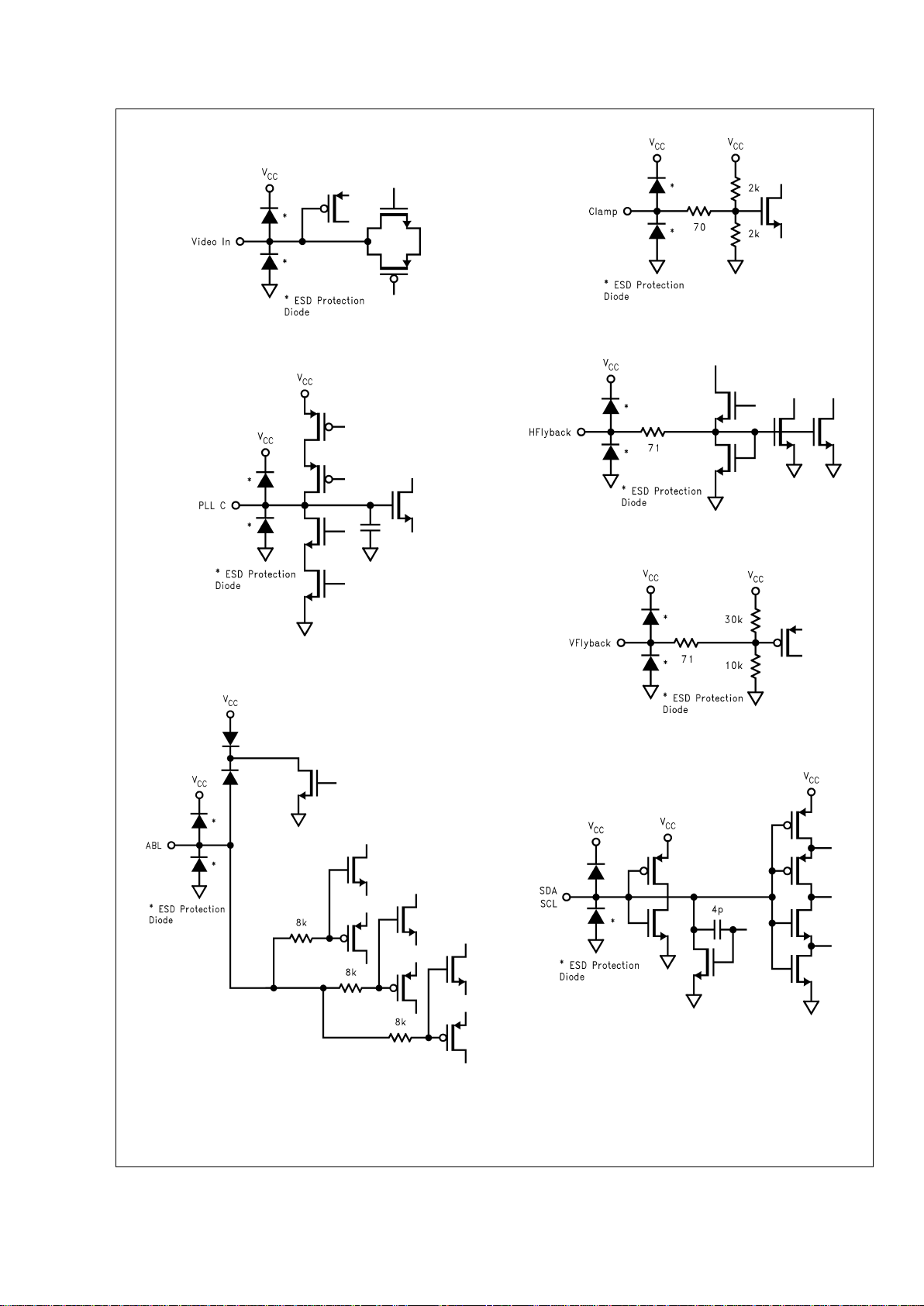
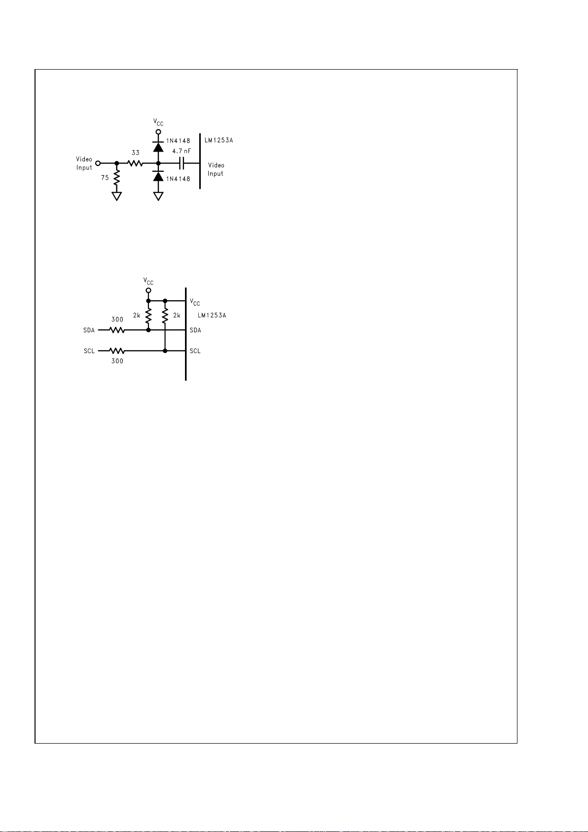
Pin 4, 5, 6 —Blue, Red, and Green Video In The red, blue,
and green video signal is AC coupled into these pins. The
value of the capacitors is very important as they also serve
DS101265-7
FIGURE 4. V Blank = 10
DS101265-8
FIGURE 5. V Blank = 63
DS101265-9
FIGURE 6. V Blank = 127
LM1253A
www.national.com 8
Pin Descriptions (Continued)
as the DC clamp control capacitors. A value of 0.0047 µF is
used in the demo boards. The schematic shown in
Figure 29
which has a series resistance of 33Ω and clamp diodes to
V
CC
and ground should be used to protect the LM1253A
from ESD. A good ground should be between the input connector and the LM1253A. The video traces should be kept
short.
Figure 29
shows the external schematic of pins 4, 5,
and 6,
Figure 14
shows the internal schematic of pins 4, 5,
and 6.
Pin 7 — Analog Ground Ground for the video section of the
LM1253A. All ground pins of the LM1253A should be connected together by a ground plane under the LM1253A. See
Figure 31
, which shows a sample layout.
Pin 8 — Analog Supply 5V supply for the video section of
the preamp. A 0.1 µF capacitor should be connected between pin 7 and pin 8, as close as possible to the LM1253A.
A 100 µF capacitor should also be connected between pin 7
and pin 8.
Pin 9— Analog Supply 5V supply for the PLL section of the
LM1253A. A 0.1 µF capacitor should be connected between
pin 9 and pin 7, as close as possible to the LM1253A.
Pin 10—PLL Ground Ground for the PLL section of the
LM1253A. Only the PLL components connected to pin 11
should be connected to this ground pin. Pin 10 should also
be connected to the ground plane under the LM1253A. All
ground pins of the LM1253A should be connected together
by a ground plane under the LM1253A. See
Figure 31
, which
shows a sample layout.
Pin 11—PLL C A resistor capacitor network is connected to
this pin. It is used to convert the charge current of the charge
pump of the PLL into a voltage that is used to control the
variable oscillator. These components should be located
very close to the LM1253A with a short ground trace to pin
10.
The recommended values are R28 = 6.2 kΩ, C23 = 0.1 µF,
and C33 = 2.2 nF. When these component values are used
the range and gain values in
Table 12
can be loaded into
register 843Eh.
An example layout is shown in
Figure 31,Figure 29
shows
the external schematic of pin 11,
Figure 15
shows the inter-
nal schematic.
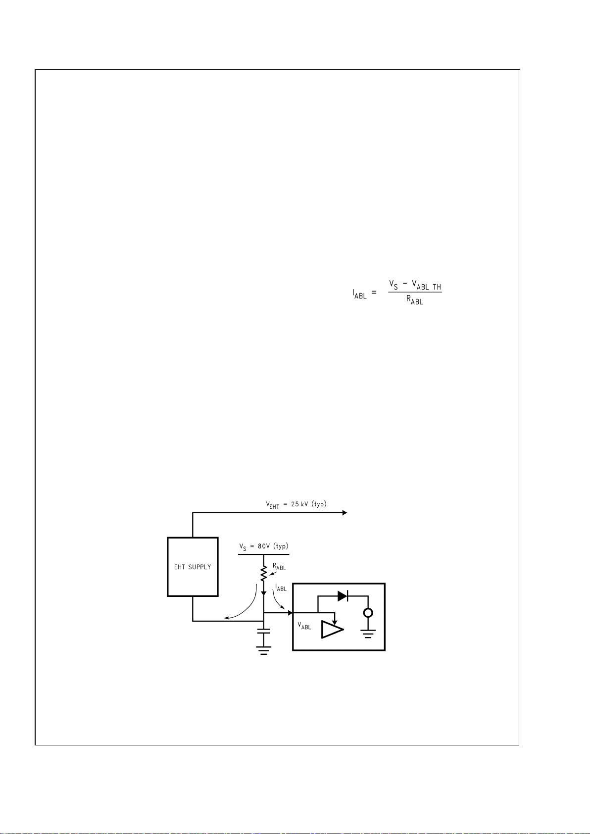
Pin 12—ABL The Auto Beam Limit control reduces the gain
of the video amplifiers in response to a control voltage proportional to the CRT beam current. The ABL acts on all three
channels in an identical manner.This is required for CRT life
and X-ray protection. The beam current limit circuit application is as shown in
Figure 7
: when no current is being drawn
by the EHT supply, current flows from the supply rail through
the ABL resistor and into the ABL input of the IC. The IC
clamps the input voltage to a low impedance voltage source
(the 5V supply rail).
When current is drawn from the EHT supply, the current
passes through the ABL resistor, and reduces the current
flowing into the ABL input of the IC.
When the EHT current is high enough, the current flowing
into the ABL input of the IC drops to zero. This current level
determines the ABL threshold and is given by:
Where:
V
S
is the external supply (usually the CRT driver supply rail,
about 80V)
V
ABL TH
is the threshold ABL voltage of the IC
R
ABL
is the ABL resistor value
I
ABL
is the ABL limit
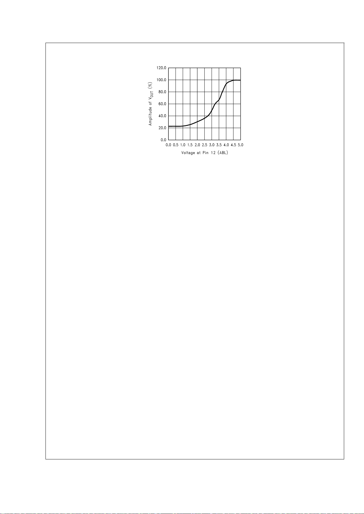
When the voltage on the ABL input drops below the ABL
threshold of the pre-amp, the gain of the pre-amp decreases,
which is shown in
Figure 8
, which reduces the beam current.
Afeedback loop is thus established which acts to prevent the
average beam current exceeding I
ABL
.
Figure 29
shows the external schematic of pin 12,
Figure 16
shows the internal schematic.
DS101265-12
FIGURE 7. ABL
LM1253A
www.national.com9
Pin Descriptions (Continued)
Pin 13—Clamp A positive going clamp signal is input on
this pin. Using this signal black level clamping of the video is
carried out directly on the input video that is AC coupled into
the high impedance preamplifier input, thus eliminating the
need for additional black level clamp capacitors.
Figure 29
shows the external schematic of pin 13,
Figure 17
shows the
internal schematic. An optional capacitor to ground may be
needed if noise interferes with the clamp signal.
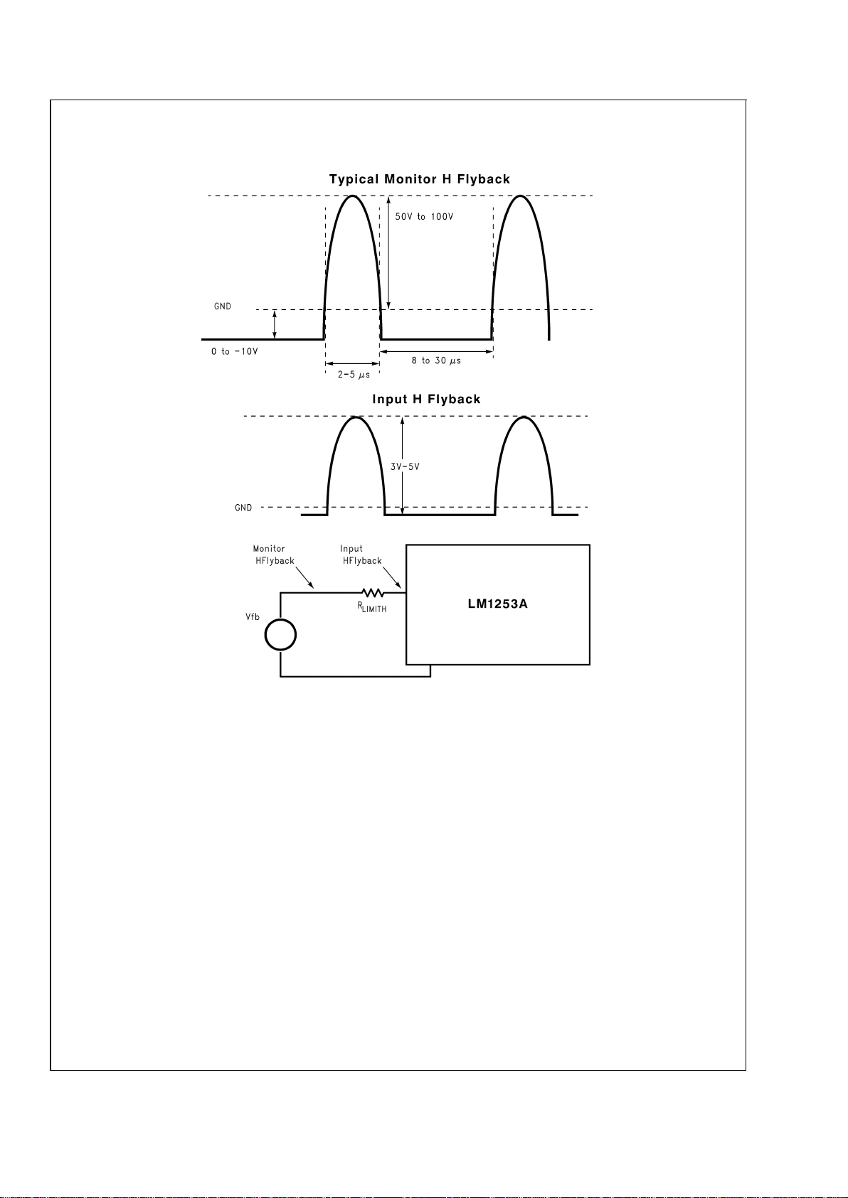
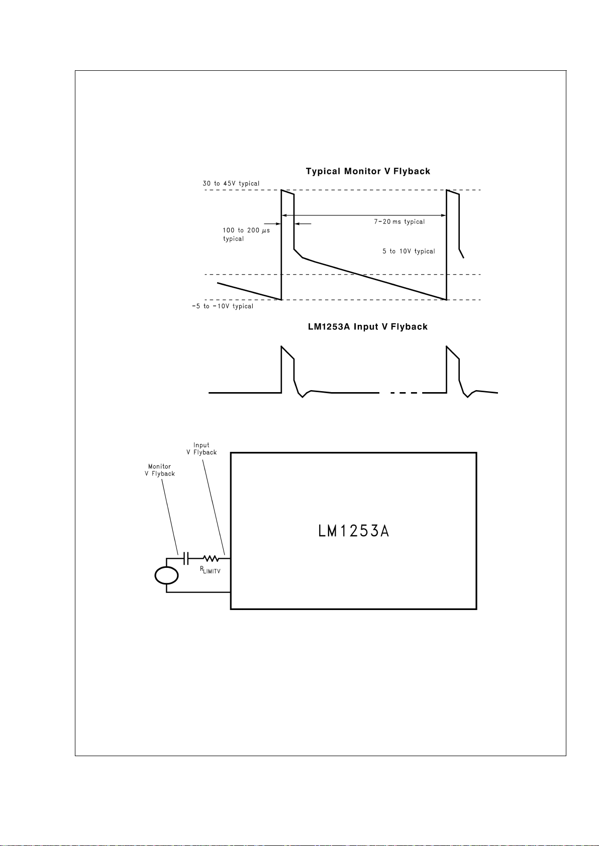
Pin 14—H Flyback H Flyback is an analog signal input from
the monitor horizontal scan. HBLANK is a digital signal derived from the horizontal flyback pulse as shown in
Figure 9
.
An optional capacitor and/or resistor to ground may be
needed if noise interferes with the H Flyback signal.
The horizontal flyback from the monitor must be a clean signal. There should be no ringing or other noise on the flyback.
DS101265-70
FIGURE 8. Effect of ABL Voltage on V
OUT
LM1253A
www.national.com 10
Pin Descriptions (Continued)
R
LIMITH
is set to limit the input current into the IC to a maximum value of +1 mA during flyback and −150 µA during normal forward scan. For example if an h flyback with a peak of
100V is used, R
LIMITH
= 100 kΩ.The internal input impedance of pin 14 is low to limit the maximum voltage swing at
the input to within the supply rail and ground. The IC interface circuit creates a digital signal from this waveform, which
is used as the blanking signal, and termed HBLANK. This
signal is used by the video amplifier for blanking the video
and by the OSD generator as the horizontal sync reference
for the PLL.
Loss of the horizontal flyback pulse implies that the monitor
is not scanning, and therefore no image is being displayed.
The HBLANK pulse is still required by the LM2453 CRT
driver in order to maintain correct bias conditions in the CRT
until the power supplies are switched off, but video will be set
at black level to prevent front of screen problems, using the
NO_VID line. See also the
Loss of Horizontal Flyback
sec-
tion.
Figure 29
shows the external schematic of pin 14,
Figure 18
shows the internal schematic.
Pin 15—V Flyback This is an analog signal from the moni-
tor vertical scan. The analog waveform is AC coupled and
fed to the input of the IC via a current limiting resistor to pre-
vent the positive and negative excursions of the signal causing excessive current or voltage swing at the input to the IC.
See
Figure 10
.
R
LIMITV
is set to limit the maximum input voltage swing into
the IC to less than the supply rails. The input to the IC is
positive edge triggered, and ignores the falling edge. Because of horizontal rate noise on the waveform, the input
buffer incorporates hysteresis, triggering at a positive going
threshold of V
VTH+
and a negative going threshold of V
VTH
.
The input buffer produces a digital signal VSTART which is
used to start the VBLANK timer. The positive rising edge of
VSTART sets a counter timer, which counts horizontal periods using the HBLANK signal. The timer resets VBLANK
when it reaches the value preset in the register VCOUNT
(set by the micro-controller over I
2
C). While the output
VBLANK is active, an AND function prevents any further
transitions on the VSTART waveform from retriggering the
counter.
The positive edge of the VSTART signal is initially transmitted through to VBLANK through an OR function, as the timer
may take up to one horizontal line period to begin timing the
duration of the pulse. The application must ensure that the
DS101265-13
FIGURE 9. H Flyback Input Pulse
LM1253A
www.national.com11
Pin Descriptions (Continued)
VFLYBACKvertical flyback pulse is kept high during that initial period to prevent the output VBLANK from switching between high and low states.
Loss of vertical flyback pulse implies that the monitor is not
scanning, and therefore no image is being displayed. The
VBLANK pulses are still required by the LM2453 CRT driver
in order to maintain correct bias conditions in the CRT until
the power supplies are switched off, but video will be set at
black level to prevent front of screen problems, using the
NO_VID line. See also the
Loss of Vertical Flyback Pulse
section.
Figure 29
shows the external schematic of pin 15,
Figure 19
shows the internal schematic.
Pin 16—SDA The I
2
C data line. A pull up resistor of about
2kΩshould be connected between this pin and +5V.A300Ω
resistor should be connected in series with the data line to
protect the IC against arcing.
Figure 29
shows the external
schematic of pin 16,
Figure 20
shows the internal schematic.
Pin 17—SCL The I
2
C clock line. A pull up resistor of about
2kΩshould be connected between this pin and +5V.A300Ω
resistor should be connected in series with the clock line to
protect the IC against arcing.
Figure 29
shows the external
schematic of pin 17,
Figure 20
shows the internal schematic.
Pin 18 — Digital Ground Ground for the OSD section of the
LM1253A. All ground pins of the LM1253A should be connected together by a ground plane under the LM1253A. See
Figure 31
, which shows a sample layout.
Pin 19 — Digital Supply 5V supply for the OSD section of
the LM1253A. A 0.1 µF capacitor should be connected between pin 18 and pin 19, as close as possible to the
LM1253A.
DS101265-5
FIGURE 10. Vertical Flyback Input Pulse
LM1253A
www.national.com 12
Pin Descriptions (Continued)
Pin 20 — Digital Supply 5V supply for the OSD section of
the LM1253A. Pins 19 and 20 should be tied together under
normal operating conditions.
Pin 21—Analog Supply 5V supply for the video section of
the preamp. A 0.1 µF capacitor should be connected between pin 21 and pin 22, as close as possible to the
LM1253A.
Pin 22—Analog Ground Ground for the video section of
the LM1253A. All ground pins of the LM1253A should be
connected together by a ground plane under the LM1253A.
See
Figure 31
, which shows a sample layout.
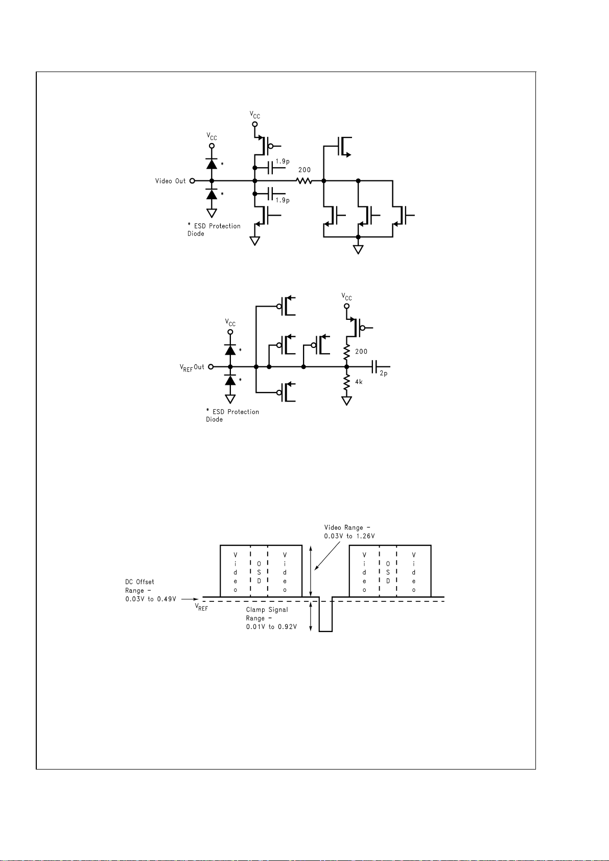
Pin 23, 24, and 25— Green, Red, and Blue Video Out
These pins output the red, green, and blue video information
in the VideoPlex format. These pins are connected to the
LM2453 using as short of traces as possible. An inductor
should be in series with the trace between the preamp and
CRT driver. The value of this inductor depends on the board
layout.
Figures 29, 30
show the external schematic of pins
23, 24, and 25,
Figure 21
shows the internal schematic.
Pin 26—V
REF
Out The voltage that the VideoPlex signal is
referenced to is output on this pin. A 0.1 µF capacitor should
be connected between this pin and ground and be located
close to the LM1253A. This pin is connected to the V
REF
pin
of the LM2453. A 0.1 µF capacitor also needs to be connected very close to the LM2453. A 100 µF capacitor should
also be connected to this trace.
Figures 29, 30
show the ex-
ternal schematic of pin 26,
Figure 22
shows the internal
schematic.
Pin 27—Analog Ground Ground for the band gap refer-
ence section of the LM1253A. All ground pins of the
LM1253A should be connected together by a ground plane
under the LM1253A. See
Figure 31
, which shows a sample
layout.
Pin 28 — Analog Supply 5V supply for the band gap refer-
ence section of the preamp. A 0.1 µF capacitor should be
connected between pin 27 and pin 28, as close as possible
to the LM1253A. See
Figure 31
, which shows a sample lay-
out.
Input/Output Schematics
DS101265-14
FIGURE 11. Pin 1 (R
EXTVREF
)
DS101265-15
FIGURE 12. Pin 2 (V Blank Out)
DS101265-16
FIGURE 13. Pin 3 (V
REF
Cap)
LM1253A
www.national.com13
Input/Output Schematics (Continued)
DS101265-17
FIGURE 14. Pins 4, 5, and 6 (Video In)
DS101265-18
FIGURE 15. Pin 11 (PLL C)
DS101265-19
FIGURE 16. Pin 12 (ABL)
DS101265-20
FIGURE 17. Pin 13 (Clamp)
DS101265-21
FIGURE 18. Pin 14 (H Flyback)
DS101265-22
FIGURE 19. Pin 15 (V Flyback)
DS101265-23
FIGURE 20. Pins 16 and 17 (SDA and SCL)
LM1253A
www.national.com 14
Input/Output Schematics (Continued)
National VideoPlex Video System
The LM1253A CRT Pre-Amp in conjunction with the LM2453
CRT driver uses the National VideoPlex multiplexed video
signal to send the video signal and DC clamp level from the
pre-amp to the CRT driver. The basic signal scheme is
shown in
Figure 23
.
The response of the LM2453 CRT driver to the VideoPlex
signal from the LM1253A Pre-Amp is shown in
Figure 24
.
Note that there are two sections in the video signal; the video
information is above V
REF
and the clamp information is be-
low V
REF
. The signals on the video out and clamp pins of the
LM2453 for an arbitrary video waveform from the LM1253A
is shown in
Figure 25
.
DS101265-24
FIGURE 21. Pins 23, 24, and 25 (Video Out)
DS101265-25
FIGURE 22. Pin 26 V
REF
Out
DS101265-26
FIGURE 23. National VideoPlex Video Signal (Pre-Amp Output)
LM1253A
www.national.com15
National VideoPlex Video System (Continued)
ESD and Arc-Over Protection
The LM1253A incorporates full ESD protection with special
consideration given to maximizing arc-over robustness. The
monitor designer must still use good circuit design and PCB
layout techniques. The human body model ESD susceptibility of the LM1253A is 2 kV,however many monitor manufacturers are now testing their monitors to the level 4 of the IEC
801-2 specification which requires the monitor to survive an
8 kV discharge. External ESD protection is needed to survive this level of ESD. The LM1253A provides excellent protection against both ESD and arc-over, but this is not a substitute for good PCB layout.
Figure 26
show the recommended input protection for the
LM1253A. This provides the best protection against ESD.
When this protection is combined with good PCB layout the
LM1253A will easily survive the IEC 801-2 level 4 testing
(8 kV ESD). It is strongly recommended that the protection
diodes be added as shown in
Figure 26
. The 1N4148 diode
has a maximum capacitance of 4 pF which will have little effect on the response of the video system due to the low impedance of the input video.
The ESD cells of the LM1253A also provide good protection
against arc-over, however good PCB layout is necessary.
The LM1253A should not be exposed directly to the voltages
that may occur during arc-over. The main vulnerability of the
LM1253A to arc-over is though the ground traces on the
PCB. For proper protection all ground connections associated with the LM1253A, including the grounds to the bypass
capacitors, must have short returns to the ground pins. Asignificant ground plane should be used to connect all the
LM1253A grounds.
Figure 31
, which shows the demo board
layout, is an excellent example of an effective ground plane.
The list below should be followed to ensure a PCB with good
grounding:
•
All grounds associated with the LM1253A should be connected together through a large ground plane.
•
CRT driver ground is connected to the video pre-amp
ground at one point.
•
CRTand arc protection grounds are connected directly to
the chassis or main ground. There is no arc-over current
flow from these grounds through the LM1253A grounds.
•
Input signal traces for SDA, SCL, H Flyback, V Flyback,
Clamp should be kept away from the LM2453 and all
traces that an arc can travel on.
•
Output signal traces of the LM1253A (video, V
BLANK
,
V
REF
) should be kept away from traces that carry the out-
put signals of the LM2453.
If any one of the above suggestions is not followed the
LM1253A may become more vulnerable to arc-over. Improper grounding is by far the most common cause of a
video pre-amp failure during arc-over.
DS101265-27
FIGURE 24. DC I/O Transfer Characteristics for the LM2453 CRT Driver
(Test Conditions: V
REF
= 1.65V, V
CC1
= 80V, VBB= 8V)
DS101265-28
FIGURE 25. LM2453 Input and Output Waveforms
LM1253A
www.national.com 16
ESD and Arc-Over Protection
(Continued)
The I
2
C specification recommends that the SDA and SCL
pins should be protected from arc-over.This is done by adding a resistor in series with each pin.
Figure 27
shows how
the resistors are connected to the SDA and SCL lines.
Pre-Amp Functional Description
Figure 1
shows the block diagram of the LM1253A. The
video signal is input to the LM1253A through the circuit
shown in
Figure 26
. Black level clamping is carried out directly on the AC coupled input signal at the input of the high
impedance buffer amplifier, thus eliminating the need for
black level clamp capacitors. The following sections then
modify the input video signal:
•
Contrast Attenuator—Sets the contrast level of the video
signal for all three channels.
•
Auto Beam Limit—Reduces the gain of all three video
amplifiers in response to a control voltage proportional to
the CRT beam current.
•
Gain Attenuator —Separately sets the gain for each
video channel.
•
Brightness—Sets the brightness for all three channels.
•
Bias—Adds an offset to the brightness controls for all
three video channels.
•
Pedestal—Adds a dc voltage offset to the brightness
control, in order that bi-directional control of the brightness control is always possible at all bias voltage settings.
•
Source Select—Switches between the input video signal
and the analog OSD signal generated by the 3 bit pallet
DAC control block.
•
DC Offset—Adds a dc voltage offset to all three video
outputs.
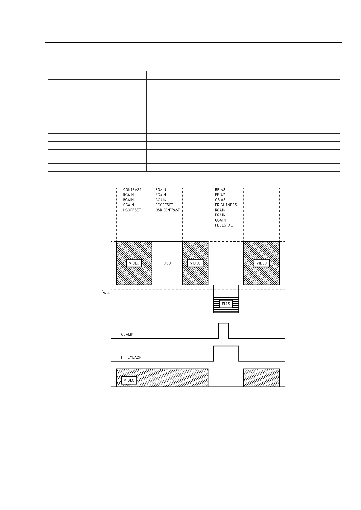
The above sections use the registers shown in
Table 2.Fig-
ure 28
shows which section of the output video and clamp
signal each register controls.
DS101265-29
FIGURE 26. Recommended Video Input ESD Protection
DS101265-30
FIGURE 27. Recommended Arc-Over Protection for
SDA and SCL Pins
LM1253A
www.national.com17
Pre-Amp Functional Description (Continued)
TABLE 2. Registers Controlling the Output Video and Clamp Signal
Parameter Address Size Description Default
BGAIN 8430h 7 Bit Blue Channel Gain 60h
GGAIN 8431h 7 Bit Green Channel Gain 60h
RGAIN 8432h 7 Bit Red Channel Gain 60h
CONTRAST 8433h 7 Bit Overall Gain of All Three Channels 60h
BBIAS 8434h 8 Bit Blue Bias Clamp Pulse Amplitude 80h
GBIAS 8435h 8 Bit Green Bias Clamp Pulse Amplitude 80h
RBIAS 8436h 8 Bit Red Bias Clamp Pulse Amplitude 80h
BRIGHTNESS 8437h 8 Bit Amplitude of Brightness Clamp Pulse of All 3 Channels 80h
PEDESTAL 8438h Bits 7–5 3 Bit Offset to the Brightness Control 4h
OSD
CONTRAST
8438h Bits 4–3 2 Bit OSD Gain 2h
DC OFFSET 8438h Bits 2–0 3 Bit Active Video DC Offset of All 3 Channels 4h
An active horizontal blanking signal is added to the video at
the output, giving excellent smear performance, and preventing video content dependent DC bias offsets as a result
of high frequency over shoot.
The outputs are referenced to a DC level (V
REF
) produced by
the LM1253A preamp, and so are guaranteed to provide
stable DC operating levels within the system without the
need for additional external feedback components.
DS101265-31
FIGURE 28. Register Control of the Output Video and Clamp Signal
LM1253A
www.national.com 18

Pre-Amp Functional Description
(Continued)
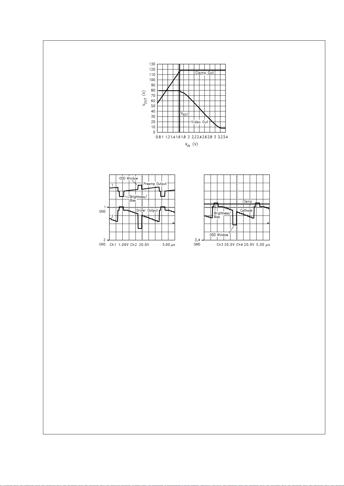
Active Video Transfer Characteristic
Gain, contrast, and DC Offset control the amplitude of the
active video. The Contrast Control range is 20 dB (10X) and
the Gain Control range is 10 dB (3.2X). The DC offset can
vary the active video output level by about 470 mV in total,
allowing a total range of adjustment of about 24V in seven
3.4V steps at the output of a typical LM2453 CRT driver.
OSD Transfer Characteristic
Gain, DC Offset, and OSD Contrast control the amplitude of
the OSD signal. The OSD is not affected by the Brightness
control, but is proportional to the Gain control, with a gain
control range of 10 dB (3.2X). The DC offset will affect the
OSD output level by 470 mV in total. The OSD Contrast will
change the amplitude of the OSD output level by 610 mV in
total.
Brightness/Bias Transfer Characteristic
Bias, Brightness, Gain, and Pedestal control the amplitude
of the brightness/bias (clamp) portion of the signal. The bias
control range sets the brightness/bias pulse between 0.12V
and 0.55V below the value of V
REF
during blanking. The bias
voltage is unaffected by changes in the other controls. The
brightness control is bi-directional and adds or subtracts an
additional amount of between –0.2V and +0.2V to the
brightness/bias pulse during blanking, when gain is set to
maximum. If gain is reduced, the brightness output voltage is
reduced in proportion to allow gain tracking of the brightness
control. The Pedestal controls the offset to the brightness
control, in order that bi-directional operation of the brightness control is always possible at all bias voltage settings.
Auto Beam Limit Control
The Auto Beam Limit control reduces the gain of the video
amplifier in response to a control voltage proportional to the
CRT beam current. It is not recommended that this input be
used as an analog contrast control.
Horizontal Phase Locked Loop
A phase locked oscillator produces a pixel clock for the OSD
generator. This oscillator takes the HBLANK signal as the
sync signal. Aprogrammable divider sets the divide ratio and
thus the number of pixels on a horizontal line.
Fault Operation
Loss of Vertical Flyback Pulse
Loss of vertical flyback pulse implies that the monitor is not
scanning, and therefore no image is being displayed. The
VBLANK pulses are still required by the LM2453 CRT driver
in order to maintain correct bias conditions in the CRT until
the power supplies are switched off, but video is set at black
level.
Note also that interlace mode is supported by the LM1253A.
In interlace mode, a frame is composed of two sequential
fields. In the first field, the odd lines are displayed. In the second field the even lines are displayed. Acomplete frame consists of an odd number of horizontal lines, so that each field
contains a half line. This will result in an alternate half line
phase difference between each field of the VFLYBACK pulse
with respect to the HBLANK pulse.
Loss of Horizontal Flyback
Loss of horizontal flyback pulse implies that the monitor is
not scanning, and therefore no image is being displayed.
The HBLANK pulse is still required by the LM2453 CRT
driver in order to maintain correct bias conditions in the CRT
until the power supplies are switched off, but video is set at
black level.
In the absence of an externally supplied horizontal flyback
pulse, the PLL will free run and generate its own HBLANK
pulse. The PLL free run pulse will be gated into the HBLANK
line to the pre-amp to allow normal operation of the pre-amp
and driver biasing.
V
CC
Detect
The V
CC
power supply will be continuously monitored by the
LM1253A. Should the V
CC
supply drop to less than V
CCDET
then the video signal will be set to V
REF
.
The device will continue to operate down to V
CCDET
, although some parameters may fall outside of specification
when the supply drops below V
CCMIN
.
Power Save Mode
Procedure To Put The LM1253A Into Power Save Mode
or Power Off Blanking
If the monitor has a power save mode the following procedure should be used to put the LM1253A into power save
mode. This should be used for both power save modes initiated from the video card and power save modes initiated by
a user on the front panel of the monitor.
1. Set Bias and Brightness registers (8434h – 8437h) to 0.
2. Set the LM1253A to blank video by setting register
8439h to 01h.
3. Turn off the 8V and 80V supply to the LM2453.
4. Set the LM1253A to power save by setting register
8439h to 02h.
LM1253A
www.national.com19

Schematics
DS101265-34
FIGURE 29. LM1253A/LM2453 Demo Board Schematic
LM1253A
www.national.com 20

Schematics (Continued)
DS101265-69
FIGURE 30. LM1253A/LM2453 Demo Board Schematic (continued)
LM1253A
www.national.com21

PCB Layout
DS101265-35
FIGURE 31. LM1253A/LM2453 Demo Board Layout
LM1253A
www.national.com 22

OSD Generator Operation
Page Operation
The block diagram of the OSD generator is shown
Figure 32
.
Video information is created using any of the 256 predefined characters stored in the mask programmed ROM.
Each character has a unique 8 bit code that is used as its address. Consecutive rows of characters make up the displayed window. These characters can be stored in the page
RAM, written under I
2
C controlled commands by the monitor
micro-controller. Each row can contain any number of characters up to the limit of the displayable line length, although
some restrictions concerning the enhanced features apply
on character rows longer than 32 characters
The number of characters across the width and height of the
page can be varied under I
2
C control, but the total number of
characters that can be stored and displayed on the screen is
limited to 512 including any row end, skip line, and window
end control characters. The horizontal and vertical start position can also be programmed under I
2
C control.
OSD Video DAC
The OSD DAC is controlled by the 9 bit (3x9 bits) OSD video
information coming from the pixel serializer look-up table.
The OSD DAC is shown in the
Figure 33
, where the gain is
programmable by the 2 bit OSD CONTRAST register, in 4
stages to give the required OSD signal.
The analog signal created by the OSD DACs is biased with
respect to V
REF
.
DS101265-36
FIGURE 32. Block Diagram of the OSD Generator
DS101265-37
FIGURE 33. Block Diagram of OSD DACs
LM1253A
www.national.com23

OSD Generator Operation (Continued)
OSD Video Timing
The OSD SELECT signal switches the source of video information within the preamplifier from external video to the internally generated OSD video.
Windows
Two separate windows can be opened, utilizing the data
stored in the page RAM. Each window has its own horizontal
and vertical start position, although the second window
should be horizontally spaced at least two character spaces
away from the first window, and should never overlap the
first window when both windows are on. The OSD window
must be placed within the active video.
Character Cell
Each character is defined as a 12 wide by 18 high matrix of
picture elements, or ‘pixels’. The character font is shown in
Figures 45, 46, 47, 48, 49, 50
. There are two types of char-
acters defined in the character ROM:
1. Two-color: There are 190 two-color characters. Each
pixel of these characters is defined by a single bit value.
If the bit value is 0, then the color is defined as ‘Color 1’
or the ‘background’ color. If the bit value is 1, then the
color is defined as ‘Color 2’, or the ‘foreground’ color.An
example of a character is shown in
Figure 34
.
2. Four-color: There are 64 four-color characters stored in
the character ROM. Each pixel of the four-color character is defined by two bits of information, and thus can define four different colors, Color 1, Color 2, Color 3, and
Color 4. Color 1 is defined as the ‘background’ color.All
other colors are considered ‘foreground’ colors, although
for most purposes, any of the four colors may be used in
any way. Because each four-color character has two
bits, the LM1253A internally has a matrix of two planes
of ROM as shown in
Figure 35
.
12 columns
18 rows
COLOR 1
COLOR 2
DS101265-38
FIGURE 34. A Two-Color Character
Plane 1 + Plane 2 = Composite
DS101265-39
FIGURE 35. A Four-Color Character
LM1253A
www.national.com 24

OSD Generator Operation (Continued)
Attribute Tables
Each character has an attribute value assigned to it in the
page RAM. The attribute value is 4 bits wide, making each
character entry in the page RAM 12 bits wide in total. The attribute value acts as an address which points to one of 16
entries in either the two-color attribute table RAM or the fourcolor attribute table RAM. The attribute word in the table contains the coding information which defines which color is represented by Color 1 and Color 2 in the two color attribute
table and Color 1, Color 2, Color 3, Color 4 in the four-color
attribute table. Each color is defined by a 9 bit value, with 3
bits assigned to each channel of RGB. A dynamic look up
table defines each of the 16 different color combination selections or ‘palettes’. As the look up table can be dynamically
coded by the micro-controller over the I
2
C interface, each
color can be assigned to any one of 2
9
(i.e. 512) choices.
This allows a maximum of 64 different colors to be used
within one page using the 4-color characters, with up to 4 different colors within any one character and 32 different colors
using the 2-color characters, with 2 different colors within
any one character.
Transparent Disable
In addition to the 9 lines of video data, a tenth data line is
generated by the transparent disable bit. When this line is
activated, the black color code will be translated as ‘transparent’ or invisible. This allows the video information from
the PC system to be visible on the screen when this is
present. Note that this feature is enabled on all black of the
first 8 attribute table entries.
Enhanced Features
In addition to the wide selection of colors for each character,
additional character features can be selected on a character
by character basis.
1. Button Boxes— The OSD generator examines the character string being displayed and if the ‘button box’ attributes have been set in the Enhanced feature byte,
then a box creator selectively substitutes the character
pixels in either or both the top and right most pixel line or
column with a button box pixel. The shade of the button
box pixel depends upon whether a ‘depressed’ or
‘raised’ box is required, and can be programmed by
I
2
C.The raised pixel color (‘highlight’) is defined by the
value in the color palette register, EF1 (normally white).
The depressed pixel (‘lowlight’) color by the value in the
color palette register EF2 (normally gray). See
Figure
36
.
2. Heavy Button Boxes—When heavy button boxes are
selected, the color palette value stored in register EF3 is
used for the depressed (‘lowlight’) pixel color instead of
the value in register EF2.
3. Shadowing—Shadowing can be added to two-color
characters by choosing the appropriate attribute value
for the character. When a character is shadowed, a
shadow pixel is added to the lower right edges of the
color 2 image, as shown in
Figure 37
. The color of the
shadow is determined by the value in the color palette
register EF3 (normally black).
4. Bordering—A border can be added to the two-color
characters. When a character is bordered, a border pixel
is added at every horizontal, vertical or diagonal transition between Color 1 and Color 2. See
Figure 38
. The
color of the border is determined by the value in the color
palette register EF3 (normally black).
5. Blinking—If blinking is enabled as an attribute, all colors
within the character except the button box pixels which
have been over-written will alternately switch to Color 1
and then back to Color 2 at a rate determined by the
micro-controller under I
2
C control.
LM1253A
www.national.com25

OSD Generator Operation (Continued)
RAISED
CHAR1
CHAR1
Bit 0
(of Previous
Character)
Line 0
(of Character
Below)
Bit 11
Bit 0
Line 0
Line 17
DS101265-40
DEPRESSED
CHAR1
CHAR1
Bit 0
(of Previous
Character)
Line 0
(of Character
Below)
Bit 11
Bit 0
Line 0
Line 17
DS101265-41
Effect on the screen:
DS101265-42
FIGURE 36. Button Boxes
DS101265-43
FIGURE 37. Shadowing
DS101265-44
FIGURE 38. Bordering
LM1253A
www.national.com 26

Micro-Controller Interface
The micro-controller interfaces to the LM1253A pre-amp via
an I
2
C interface. The protocol of the interface begins with a
Start Pulse followed by a byte comprised of a seven bit Slave
Device Address and a Read/Write bit. Since the first byte is
composed of both the address and the read/write bit the address of the LM1253A for writing is BAh (1011 1010) and the
address for reading is BBh (1011 1011). The development
software provided by National Semiconductor will automatically take care of the difference between the read and write
addresses if the target address under the communications
tab is set to BAh.
Figures 39, 40
show a write and read se-
quence across the I
2
C interface.
Write Sequence
The write sequence begins with a start condition which consists of the master pulling SDA low while SCL is held high.
The slave device address is next sent. The address byte is
made up of an address of seven bits (7-1) and the read/write
bit (0). Bit 0 is low to indicate a write operation. Each byte
that is sent is followed by an acknowledge. When SCL is
high the master will release the SDAline. The slave must pull
SDAlow to acknowledge. The register to be written to is next
sent in two bytes, the least significant byte being sent first.
The master can then send the data, which consists of one or
more bytes. Each data byte is followed by an acknowledge
bit. If more than one data byte is sent the data will increment
to the next address location. See
Figure 39
.
Read Sequence
Read sequences are comprised of two I
2
C transfer sequences: The first is a write sequence that only transfers the
two byte address to be accessed. The second is a read sequence that starts at the address transferred in the previous
address only write access and increments to the next address upon every data byte read. This is shown in
Figure 40
.
DS101265-45
FIGURE 39. I2C Write Sequence
LM1253A
www.national.com27

Micro-Controller Interface (Continued)
The write sequence consists of the Start Pulse, the Slave
Device Address, the Read/Write bit (a zero, indicating a
write) and the Acknowledge bit; the next byte is the least significant byte of the address to be accessed, followed by its
Acknowledge bit. This is then followed by a byte containing
the most significant address byte, followed by its Acknowledge bit. Then a Stop bit indicates the end of the address
only write access.
Next the read data access will be performed beginning with
the Start Pulse, the Slave Device Address, the Read/Write
bit (a one, indicating a read) and the Acknowledge bit. The
next 8 bits will be the read data driven out by the LM1253A
pre-amp associated with the address indicated by the two
address bytes. Subsequent read data bytes will correspond
to the next increment address locations.
Read data from the LM1253A only when both OSD windows
are disabled.
DS101265-46
FIGURE 40. I2C Read Sequence
LM1253A
www.national.com 28

LM1253A Address Map
TABLE 3. Character ROM Address Map
Address
Range
R/W Description
CHARACTER ROM
0000h–2FFFh R ROM Character Fonts, 190 two-color Character Fonts that are read-only.
The format of the address is as follows:
A15–A14: Always zeros.
A13–A6: Character value (00h–BFh are valid values)
A5–A1: Row of the character (00h–11h are valid values)
A0: Low byte of line when a zero. High byte of line when a one.
The low byte will contain the first eight pixels of the line with data Bit 0 corresponding to the left
most bit in the Character Font line. The high byte will contain the last four pixels and data Bits
7–4 are “don’t cares”. Data Bit 3 of the high byte corresponds to the right most pixel in the
Character Font line.
3000h–3FFFh R ROM Character Fonts, 64 four-color Character Fonts that are read-only.
The format of the address is as follows:
A15–A14: Always zeros.
A13–A6: Character value (C0h–FFh are valid values)
A5–A1: Row of the character (00h–11h are valid values)
A0: Low byte of line when a zero. High byte of line when a one.
The low byte will contain the first eight pixels of the line with data Bit 0 corresponding to the left
most bit in the Character Font line. The high byte will contain the last four pixels and data Bits
7–4 are “don’t cares”. Data Bit 3 of the high byte corresponds to the right most pixel in the
Character Font line.
NOTE: The value of Bit 0 of the Character Font Access Control Register (I
2
C Address 8402h) is a
zero, it indicates that the Bit 0 data value of the four-color pixels is being accessed via these
addresses. When the value of Bit 0 of the Access Control Register is a one, it indicates that the
Bit 1 data value of the four-color pixel is being accessed via these addresses.
4000h–7FFFh RESERVED.
TABLE 4. Display Page RAM Address Map
Address
Range
R/W Description
DISPLAY PAGE RAM
8000h–81FF R/W Display Page RAM Characters. A total of 512 display characters, skipped line, end-of-row and
end-of-window character codes may be supported via this range.
To support skipped lines and character attributes a number of special case rules are used when
writing to this range. (Refer to the
Display Page RAM
section of this document for more details.)
LM1253A
www.national.com29

Pre-Amp Interface Registers
TABLE 5. OSD Interface Registers
LM1253A OSD Interface Registers
Register Address Default D7 D6 D5 D4 D3 D2 D1 D0
Fonts-2 Color 0000–2FFE PIXEL[7:0]
+1 XXXX PIXEL[11:8]
Fonts-4 Color 3000–3FFE PIXEL[7:0]
+1 XXXX PIXEL[11:8]
Display Page 8000–83FF CHAR_CODE[7:4] or reserved CHAR_CODE[3:0] or ATTR_CODE
FRMCTRL1 8400 10h X X X TD CDPR D2E D1E OSE
FRMCTRL2 8401 80h PIXELS_PER_LINE[2:0] BLINK_PERIOD[4:0]
CHARFONTACC 8402 00h XXXXXXATTR FONT4
VBLANKDUR 8403 10h X VBLANK_DURATION[6:0]
CHARHTCTRL 8404 51h CHAR_HEIGHT[7:0]
BBHLCTRLB0 8405 FFh B[1:0] G[2:0] R[2:0]
BBHLCTRLB1 8406 01h XXXXXXXB[2]
BBLLCTRLB0 8407 00h B[1:0] G[2:0] R[2:0]
BBLLCTRLB1 8408 00h XXXXXXXB[2]
CHSDWCTRLB0 8409 00h B[1:0] G[2:0] R[2:0]
CHSDWCTRLB1 840A 00h XXXXXXXB[2]
ROMSIGCTRL 840D 00h XXXXXXXCRS
ROMSIGDATAB0 840E 00h CRC[7:0]
ROMSIGDATAB1 840F 00h CRC[15:8]
HSTRT1 8410 13h HPOS[7:0]
VSTRT1 8411 14h VPOS[7:0]
COLWIDTH1B0 8414 00h COL[7:0]
COLWIDTH1B1 8415 00h COL[15:8]
COLWIDTH1B2 8416 00h COL[23:16]
COLWIDTH1B3 8417 00h COL[31:24]
HSTRT2 8418 56h HPOS[7:0]
VSTRT2 8419 5Bh VPOS[7:0]
W2STRTADRL 841A 00h ADDR[7:0]
W2STRTADRH 841B 01h XXXXXXXADDR[8]
COLWIDTH2B0 841C 00h COL[7:0]
COLWIDTH2B1 841D 00h COL[15:8]
COLWIDTH2B2 841E 00h COL[23:16]
COLWIDTH2B3 841F 00h COL[31:24]
Note: Set Reserved bits to 0.
LM1253A
www.national.com 30

Pre-Amp Interface Registers (Continued)
TABLE 6. Pre-Amp Interface Registers
LM1253A Pre-Amp Interface Registers
Register Address Default D7 D6 D5 D4 D3 D2 D1 D0
BGAINCTRL 8430 60h X BGAIN[6:0]
GGAINCTRL 8431 60h X GGAIN[6:0]
RGAINCTRL 8432 60h X RGAIN[6:0]
CONTRCTRL 8433 60h X CONTRAST[6:0]
BBIASCTRL 8434 80h BBIAS[7:0]
GBIASCTRL 8435 80h GBIAS[7:0]
RBIASCTRL 8436 80h RBIAS[7:0]
BRIGHTCTRL 8437 80h BRIGHTNESS[7:0]
DCOFFSET 8438 94h PEDESTAL[2:0] OSD CONT[1:0] DC OFFSET[2:0]
GLOBALCTRL 8439 00h XXXXXXPSBV
PLLFREQRNG 843E 16h X X IVIGAIN[1:0] X X PFR[1:0]
SRTSTCTRL 843F 00h X AID XXXXXSRST
Note: Set Reserved bits to 0.
Two-Color Attribute Table
TABLE 7. Two-Color Attribute Registers
LM1253A Two-Color Attribute Registers
Register Address D7 D6 D5 D4 D3 D2 D1 D0
ATT2C0n 8440 +
(n*4)
C1B[1:0] C1G[2:0] C1R[2:0]
ATT2C1n +1 C2B[0] C2G[2:0] C2R[2:0] C1B[2]
ATT2C2n +2 X X EF[3:0] C2B[2:1]
ATT2C3n +3 XXXXXXXX
Note: Set Reserved bits to 0.
Two-colordisplay characterAttribute Table.The attributes for two-color display characters may be written or read via the following
address format:
A15–A6: Always 1000_0100_01b.
A5–A2: Attribute code (0h-Fh are valid values), n
A1–A0: Determines which of the 3 bytes is to be accessed.
NOTE: In the table, n indicates the attribute number 0
<=n<
=15
NOTE: When writing, bytes 0 through 2 must be written, in that order. Bytes 0 through 2 will take effect after byte 2 is written.
Since byte 3 contains all reserved bits, this byte may be written, but no effect will result.
When reading, it is OK to read only one, two, or all three bytes.
If writing more than one 2-color attributes using the auto increment feature, all four bytes must be written.
Four-Color Attribute Table
TABLE 8. Four-Color Attribute Registers
LM1253A Four-Color Attribute Registers
Register Address D7 D6 D5 D4 D3 D2 D1 D0
ATT4C0n 8500 +
(n*8)
C1B[1:0] C1G[2:0] C1R[2:0]
ATT4C1n +1 C2B[0] C2G[2:0] C2R[2:0] C1B[2]
ATT4C2n +2 X X EF[3:0] C2B[2:1]
LM1253A
www.national.com31

Four-Color Attribute Table (Continued)
TABLE 8. Four-Color Attribute Registers (Continued)
LM1253A Four-Color Attribute Registers
Register Address D7 D6 D5 D4 D3 D2 D1 D0
ATT4C3n +3 XXXXXXXX
ATT4C4n +4 C3B[1:0] C3G[2:0] C3R[2:0]
ATT4C5n +5 C4B[0] C4G[2:0] C4R[2:0] C3B[2]
ATT4C6n +6 XXXXXX C4B[2:1]
ATT4C7n +7 XXXXXXXX
Note: Set Reserved bits to 0.
Four-color display character Attribute Table. The attributes for four-color display characters may be written or read via the following address format:
A15–A7: Always 1000_0101_0b
A6–A3: Attribute value (0h–Fh are valid values), n
A2–A0: Determine which of the six bytes of the attribute is to be accessed.
NOTE: In the table, n indicates the attribute number, 0
<=n<
=15
NOTE: When writing, bytes 0 to 2 must be written, in that order and bytes 4 to 6 must be written, in that order.
Bytes 0 through 2 will take effect after byte 2 is written. Bytes 4 through 6 will take effect after byte 6 is written.
Since bytes 5 and 7 contain all reserved bits, these bytes may be written, but no effect will result. When reading, it is OK to read
only one, two, or all three bytes.
If writing more than one 4-color attributes using the auto increment feature, all eight bytes must be written.
Display Page RAM
The OSD Window
The Display Page RAM contains all of the 8 bit display character codes and their associated 4 bit attribute codes, and the special
12 bit page control codes—the row-end, skip-line parameters and window-end characters.
The LM1253A has a distinct advantage over many OSD generators that it allows variable size and format windows. The window
size is not dictated by a fixed geometry area of RAM. Instead, 512 locations of 12 bit words are allocated in RAM for the definition
of the windows, with special control codes to define the window size and shape.
Window width can be any length supported by the number of pixels per line that is selected divided by the number of pixels in a
character line. It must be remembered that OSD characters displayed during the monitor blanking time will not be displayed on
the screen, so the practical limit to the number of horizontal characters on a line is reduced by the number of characters within
the horizontal blanking period.
Character Code And Attribute Code
Each of the 512 x 12 bit locations in the page RAM is comprised of an 8 bit character or control code, and a 4 bit attribute code:
Bits 11–4 Character Code: These 8 bits define which of the 254 characters is to be called from the character ROM. Valid char-
acter codes are 02h–FFh.
Bits 3–0: Attribute code. These 4 bits address the attribute table used to specify which of the 16 locations in RAM specify the
colors and enhanced features to be used for this particular character. Two separate attribute tables are used, one for
2-color characters, the other for 4-color characters.
Each of the characters are stored in sequence in the page RAM. Special codes are used between lines to show where one line
ends and the next begins, and also to allow blank (or ‘skipped’) lines to be added between character rows.
DS101265-47
LM1253A
www.national.com 32

Display Page RAM (Continued)
Row End Code
To signify the end of a row of characters, a special ‘Row-End’ (RE) code is used in place of a character code.
Bits 11–4 Row-End Code: A special character code of 01h
Bits 3–0: Don’t care
The RE character tells the OSD generator that the character codes following must be placed on a new row in the displayed win-
dow.
Skipped Line Parameters
Each displayed row of characters may have up to 15 skipped (i.e., blank) lines beneath it in order to allow finer control of the vertical spacing of character rows. (Each skipped line is treated as a single auto-height character pixel line, so multiple scan lines
may actually be displayed in order to maintain accurate size relative to the character cell— see section
Constant Character
Height Mechanism
).
To specify the number of skipped lines, the first character in each new row of characters to be displayed is interpreted differently
than the other characters in the row. Instead of interpreting the data in the location as a character code, the information of the
12 bit word is defined as follows:
Bits 11–8 Reserved.
Bits 7–4: Skipped Lines. These four bits determine how many blank pixel lines will be inserted between the present row of dis-
play characters and the next row of display characters. A range of 0–15 may be selected.
Bits 3–0: Attribute code. The pixels in the skipped lines will normally be Color 1 of the addressed 2-Color Attribute Table entry.
Note that the pixels in the first line immediately below the character may be overwritten by the pixel override system
that creates the button box. (Refer to the
Button Box Formation
Section for more information.)
Each new line MUST start with an SL code, even if the number of skipped lines to follow is zero. An SL code MUST always follow
an RE control code.
An RE code may follow an SL code if several ‘transparent’ lines are required between sections of the window (see example 3 below). In this case, skipped lines of zero characters are displayed, causing a break in the window.
Window-End Code
To signify the end of the window, a special ‘Window-End’ (WE) code is used in place of a Row-End code.
Bits 11–4 Window-End Code: A special character code of 00h
Bits 3–0: Don’t care
The WE control code tells the OSD generator that the character codes following belong to another displayed window at the next
window location. A WE control code may follow normal characters or an SL parameter, but never an RE control code.
Writing To The Page RAM
The Display Page RAM can contain up to 512 of the above listed characters and control codes. Each character, or control code
will consume one of the possible 512 locations. For convenience, a single write instruction to bit 3 of the Frame Control Register
(8400h) can reset the page RAM value to all zero.
Display Window 1 will also start at the first location (corresponding to the I
2
C address 8000h). This location must always contain
the Skip-Line (SL) parameters associated with the first row of Display Window 1. Subsequent locations should contain the characters to be displayed on row 1 of Display Window 1, until the RE character code or WE character code is written into the Display
Page-RAM.
DS101265-48
DS101265-49
DS101265-50
LM1253A
www.national.com33

Display Page RAM (Continued)
The skip-line parameters associated with the next row must always be written to the location immediately after the preceding
row’s row-end character. The only exception to this rule is when a window-end character (value 00h) is encountered. It is important to note that a row-end character should not precede a window-end character (otherwise the window-end character will be interpreted as the next row’s skip-line parameters). Instead, the window-end character will both end the row and the window making
it unnecessary to precede it with a row-end character.
The I
2
C Format for writing a sequence of display characters is minimized by allowing sequential characters with the same at-
tribute code to be sent in a string as follows:
Byte
#
1—I2C Slave Address
Byte
#
2—LSB Address
Byte
#
3—MSB Address
Byte
#
4—Attribute Table Entry to use for the following characters
Byte
#
5—First display character, SL parameter, RE or WE control code.
Byte
#
6—Second display character, SL parameter, RE or WE control code.
Byte
#
7—Third display character, SL parameter, RE or WE control code.
.
.
Byte
#
n—Last display character in this color sequence, SL parameter, RE or WE control code to use the associated Attribute
Table Entry.
The Attribute Table Entry (Byte #4, of the above) is automatically associated with each subsequent display character or SL code
written. The following are examples of how the Display Page RAM associates to the actual On-Screen Display Window #1.
EXAMPLE #1:
A 3 X 3 character matrix of white characters on a black background is to be displayed using 2-color character codes:
The actual On-Screen Display of Window #1 is shown in
Figure 41
. Note the dotted white lines are not shown on the monitor.
They are shown here to show where the character ends.
Notes:
•
Every row must begin with an attribute and a SL. Display
Page RAM memory location 8000h will always be associated with the SL of row 0 of Display Window #1.
•
Every row except the last row of a Display Window must
end with an RE character. The character immediately after an RE character is always the SL value for the next
row.
•
The last row in a Display Window must be a WE character. The WE character must NOT be preceded by an RE
character.
•
The entire Display Window may be written in a single I2C
write sequence because the Attribute Table entry (i.e., the
color palette) does not change for the entire Display Window.
•
The Attribute Table Entry that is associated with RE and
WE characters are “don’t cares”. In general it is most efficient just to allow them to be the same value as the Attribute Table Entry associated with the previous display
character.
•
The colors of the characters and background can be
stored in a single location in the 2-color attribute table, in
location ATT0.
•
The data shown in
Table 9
is sent to the LM1253A in one
I
2
C transmission.
DS101265-51
FIGURE 41. Example 1 OSD
LM1253A
www.national.com 34

Display Page RAM (Continued)
TABLE 9. Example 1 I
2
C Transmission
Command
Sent
(hex)
Description
RAM Address
of the Character
or Command
I
2
C start condition (See the
Micro-Controller Interface
Section)
BA Chip address (See the
Micro-Controller Interface
Section)
00 Address LSB
80 Address MSB
00 Use Attribute table 00 for the following characters
00 Skip 0 lines 8000
02 Character “A” 8001
03 Character “B” 8002
04 Character “C” 8003
01 Row end 8004
00 Skip 0 lines 8005
05 Character “D” 8006
06 Character “E” 8007
07 Character “F” 8008
01 Row end 8009
00 Skip 0 lines 800A
08 Character “G” 800B
09 Character “H” 800C
0A Character “I” 800D
00 Window end 800E
I
2
C stop condition (See the
Micro-Controller Interface
Section)
EXAMPLE
#
2:
A 3X3 character matrix of characters on a black background is to be displayed on the screen, using 2-color character codes.
2 skipped lines are required below the first line of characters, 3 skipped lines are required below the second line of characters,
and 4 skipped lines are required below the third line of characters. The first line of characters will use color attribute 0, the second
line will use color attribute 1, the third line will use color attribute 0 for the first character, color attribute 1 for the second character,
and color attribute 2 for the third character. This is shown in
Figure 42
.
LM1253A
www.national.com35

Display Page RAM (Continued)
Notes:
•
Every row must begin with an attribute and a SL value.
Display Page RAM memory location 8000h will always be
associated with the SL of row 0 of Display Window #1.
•
If an I2C transmission finishes without an RE (in the
middle of a row) the first byte sent in the next I
2
C trans-
mission is the attribute.
•
Every row except the last row of a Display Window must
end with an RE character. The character immediately after an RE character is always the SL value for the next
row.
•
The last row in a Display Window must be a WE character. The WE character must NOT be preceded by an RE
character.
•
The data shown in
Table 10
is sent to the LM1253A in five
I
2
C transmissions.
TABLE 10. Example 2 I
2
C Transmissions
Command
Sent
(hex)
Description
RAM Address of
the Character
or Command
I
2
C start condition (See the
Micro-Controller Interface
Section)
BA Chip address (See the
Micro-Controller Interface
Section)
00 Address LSB
80 Address MSB
00 Use Attribute table 00 for the following characters
02 Skip 2 lines 8000
02 Character “A” 8001
03 Character “B” 8002
04 Character “C” 8003
01 Row end 8004
I
2
C stop condition (See the
Micro-Controller Interface
Section)
I
2
C start condition (See the
Micro-Controller Interface
Section)
BA Chip address (See the
Micro-Controller Interface
Section)
05 Address LSB
80 Address MSB
DS101265-52
FIGURE 42. Example 2 OSD
LM1253A
www.national.com 36

Display Page RAM (Continued)
TABLE 10. Example 2 I
2
C Transmissions (Continued)
Command
Sent
(hex)
Description
RAM Address of
the Character
or Command
01 Use Attribute table 01 for the following characters
03 Skip 3 lines 8005
05 Character “D” 8006
06 Character “E” 8007
07 Character “F” 8008
01 Row end 8009
I
2
C stop condition (See the
Micro-Controller Interface
Section)
I
2
C start condition (See the
Micro-Controller Interface
Section)
BA Chip address (See the
Micro-Controller Interface
Section)
0A Address LSB
80 Address MSB
00 Use Attribute table 00 for the following characters
04 Skip 4 lines 800A
08 Character “G” 800B
I
2
C stop condition (See the
Micro-Controller Interface
Section)
I
2
C start condition (See the
Micro-Controller Interface
Section)
BA Chip Address
0C Address LSB
80 Address MSB
01 Use Attribute table 01 for the following characters
09 Character “H” 800C
I
2
C stop condition (See the
Micro-Controller Interface
Section)
I
2
C start condition (See the
Micro-Controller Interface
Section)
BA Chip address (See the
Micro-Controller Interface
Section)
0D Address LSB
80 Address MSB
02 Use Attribute table 02 for the following characters
0A Character “I” 800D
00 Window end 800E
I
2
C stop condition (See the
Micro-Controller Interface
Section)
EXAMPLE #3:
Twodifferent length rows of characters with a black background are to be displayed on the screen, using 2-color character codes.
3 transparent skipped lines are required between the character rows. This is shown in
Figure 43
.
LM1253A
www.national.com37

Display Page RAM (Continued)
Notes:
•
In order to centralize the three characters above the five
characters on the row below, a ‘transparent’ blank character has been used as the first character on the row.
•
In order to create the transparent skipped lines between
the two character rows, a row of no characters has been
used, resulting in an RE, SL, RE, SL control code sequence.
•
In this example, the transparent character is defined by
the 2-color attribute table entryATT0. Bit 4 of Frame Control Register 1 must be set to indicate that the black color
is to be translated as transparent (see
Control Register
Definitions
section). Setting the transparent bit will make
any black in ATT0–ATT7 transparent.
•
The top row of characters are white on black; in this example, these are defined by the 2-color attribute table entry ATT9.
•
The second row of characters are gray on black; in this
example, these are defined by the 2-color attribute table
entry ATT10.
•
The black background of the characters are not transparent because ATT9 and ATT10 are used.
•
The data shown in
Table 11
is sent to the LM1253A in
four I
2
C transmissions.
DS101265-53
FIGURE 43. Example 3 OSD
LM1253A
www.national.com 38

Display Page RAM (Continued)
TABLE 11. Example 3 I
2
C Transmissions
Command
Sent
(hex)
Description
RAM Address of
the Character
or Command
I
2
C start condition (See the
Micro-Controller Interface
Section)
BA Chip address (See the
Micro-Controller Interface
Section)
00 Address LSB
80 Address MSB
00 Use Attribute table 00 for the following characters
00 Skip 0 lines 8000
80 Character “ ” 8001
I
2
C stop condition (See the
Micro-Controller Interface
Section)
I
2
C start condition (See the
Micro-Controller Interface
Section)
BA Chip address (See the
Micro-Controller Interface
Section)
02 Address LSB
80 Address MSB
09 Use Attribute table 09 for the following characters
02 Character “A” 8002
03 Character “B” 8003
04 Character “C” 8004
01 Row end 8005
I
2
C stop condition (See the
Micro-Controller Interface
Section)
I
2
C start condition (See the
Micro-Controller Interface
Section)
BA Chip address (See the
Micro-Controller Interface
Section)
06 Address LSB
80 Address MSB
00 Use Attribute table 00 for the following characters
03 Skip 3 lines 8006
01 Row end 8007
I
2
C stop condition (See the
Micro-Controller Interface
Section)
I
2
C start condition (See the
Micro-Controller Interface
Section)
BA Chip address (See the
Micro-Controller Interface
Section)
08 Address LSB
80 Address MSB
0A Use Attribute table 0A for the following characters
00 Skip 0 lines 8008
05 Character “D” 8009
06 Character “E” 800A
07 Character “F” 800B
08 Character “G” 800C
09 Character “H” 800D
00 Window end 800E
I
2
C stop condition (See the
Micro-Controller Interface
Section)
LM1253A
www.national.com39

Control Register Definitions
OSD INTERFACE REGISTERS
Frame Control Register 1 (I
2
C address 8400h).
REGISTER NAME: FRMCTRL1
Bit 7 Bit 0
RSV RSV RSV TD CDPR D2E D1E OsE
Bit 0: On-Screen Display Enable. The On-Screen Display will be disabled when this bit is a zero. When this bit is a one the
On-Screen Display will be enabled and Display Window 1 will be enabled if Bit 1 of this register is a one; likewise Display Window 2 will be enabled if Bit 2 of this register is a one.
Bit 1: Display Window 1 Enable. When Bit 0 of this register and this bit are both ones, Display Window 1 is enabled. If either
bit is a zero, then Display Window 1 will be disabled.
Bit 2: Display Window 2 Enable. When Bit 0 of this register and this bit are both ones, Display Window 2 is enabled. If either
bit is a zero, then Display Window 2 will be disabled.
Bit 3: Clear Display Page RAM. Writing a one to this bit will result in setting all of the Display Page RAM values to zero. This
bit is automatically cleared after the operation is complete.
Bit 4: Transparent Disable. When this bit is a zero, a palette color of black (ie color palette look-up table value of ‘000 000
000’) in the first 8 palette look-up table address locations (i.e., ATT = 0h–7h) will be translated as transparent. When
this bit is a one, the color will be translated as black.
Bits 7–4: RESERVED.
Frame Control Register 2 (I
2
C address 8401h).
REGISTER NAME: FRMCTRL2
Bit 7 Bit 0
PL2 PL1 PL0 BP4 BP3 BP2 BP1 BP0
Bits 4–0: Blinking Period. These five bits set the blinking period of the blinking feature, which is determined by multiplying the
value of these bits by 8, and then multiplying the result by the vertical field rate.
Bits 7–5: Pixels per Line. These three bits determine the number of pixels per line.
Bits 7–5 Description Max Fh
000b 512 pixels per line 125 kHz
001b 576 pixels per line 119 kHz
010b 640 pixels per line 112 kHz
011b 704 pixels per line 106 kHz
100b 768 pixels per line 100 kHz
101b 832 pixels per line 93 kHz
110b 896 pixels per line 87 kHz
111b 960 pixels per line 81 kHz
Character Font Access Control Register (I
2
C address 8402h).
REGISTER NAME: CHARFONTACC
Bit 7 Bit 0
RSV RSV RSV RSV RSV RSV C/A Bit
Bit 0: Four-color pixel data value Bit indicator. This bit indicates if Bit 0 (when a zero) or Bit 1 (when a one) of the four-color
pixel data value is being accessed via I
2
C addresses 3000h–3FFFh.
Bit 1: Character/Attribute Code Indicator. This bit controls what value is read via I
2
C reads of the Display Page RAM (address range 8000h–81FFh). When this bit is a 0, such reads will return the character code. When this bit is a 1, the
attribute code will be returned.
Bits 7–2: RESERVED.
LM1253A
www.national.com 40

Control Register Definitions (Continued)
Vertical Blank Duration Control Register (I
2
C address 8403h).
REGISTER NAME: VBLANKDUR
Bit 7 Bit 0
RSV VB6 VB5 VB4 VB3 VB2 VB1 VB0
Bits 6–0: Vertical Blank Duration. These seven bits set the duration of the VBLANK signal in numbers of horizontal scan lines.
Bit 7: RESERVED.
OSD Character Height Control Register (I
2
C address 8404h).
REGISTER NAME: CHARHTCTRL
Bit 7 Bit 0
CH7 CH6 CH5 CH4 CH3 CH2 CH1 CH0
Bits 7–0: Character Height: this register sets the character height according to the constant character height mechanism de-
scribed in section Constant Character Height Mechanism. The value programmed in the register is equal to the approximate number of OSD height compensated lines required on the screen divided by 4. The value is only approximate, due to the approximation used in scaling the characters.
Example: If approximately 384 OSD lines are required on the screen (regardless of the number of image lines) then
the Character Height Control Register is programmed with the value of 81.
Button Box Highlight Color Register (EF1) (I
2
C address 8405h–8406h).
REGISTER NAME: BBHLCTRLB1 (8406h) BBHLCTRLB0 (8405h)
Bit 15 Bit 8 Bit 7 Bit 0
RSV RSV RSV RSV RSV RSV RSV R2 R1 R0 B2 B1 B0 G2 G1 G0
Bits 8–0: Button Box highlight color.This register indicates the value of Enhanced Feature (button box highlight) register EF1.
Bits 15–9: RESERVED.
Button Box Lowlight Color Register (EF2) (I
2
C address 8407h–8408h).
REGISTER NAME: BBLLCTRLB1 (8408h) BBLLCTRLB0 (8407h)
Bit 15 Bit 8 Bit 7 Bit 0
RSV RSV RSV RSV RSV RSV RSV R2 R1 R0 B2 B1 B0 G2 G1 G0
Bits 8–0: Button Box lowlight color. This register indicates the value of Enhanced Feature (button box lowlight) register EF2.
Bits 15–9: RESERVED.
Heavy Button Box Lowlight/Shadow/Shading Color Register (EF3) (I
2
C address 8409h–840Ah).
REGISTER NAME: CHSDWCTRLB1 (840Ah) CHSDWCTRLB0 (8409h)
Bit 15 Bit 8 Bit 7 Bit 0
RSV RSV RSV RSV RSV RSV RSV R2 R1 R0 B2 B1 B0 G2 G1 G0
Bits 8–0: Heavy Button Box lowlight/shadow color. This register indicates the value of Enhanced Feature (heavy button box
lowlight or shadow/shading) register EF3.
Bits 15–9: RESERVED.
LM1253A
www.national.com41

Control Register Definitions (Continued)
ROM Signature Control Register (I
2
C address 840Dh).
REGISTER NAME: ROMSIGCTRL
Bit 7 Bit 0
RSV RSV RSV RSV RSV RSV RSV CRS
Bit 0: Calculate ROM Signature. Setting this bit causes the entire ROM to be read, sequentially,and a 16 bit CRC calculated
over its contents. The residual value from this calculation is placed in the ROM Signature Data register. This bit automatically clears itself when the calculation has been completed.
Bits 7–1: RESERVED.
ROM Signature Data Register (I
2
C address 840Eh–840Fh).
REGISTER NAME: ROMSIGDATAB1 (840Fh) ROMSIGDATAB0 (840Eh)
Bit 15 Bit 8 Bit 7 Bit 0
CRC15 CRC14 CRC13 CRC12 CRC11 CRC10 CRC9 CRC8 CRC7 CRC6 CRC5 CRC4 CRC3 CRC2 CRC1 CRC0
Bits 15–0: ROM Signature Data. This register indicates the residual value from the CRC calculation. Devices containing ROMs
with different programming will give different signatures. Devices with the same ROM programming will give the same
signature.
Display Window 1 Horizontal Pixel Start Location Register (I
2
C address 8410h).
REGISTER NAME: HSTRT1 (8410h)
Bit 7 Bit 0
1H7 1H6 1H5 1H4 1H3 1H2 1H1 1H0
Bits 7–0: Display Window 1 Horizontal Pixel Start Location. These seven bits determine the starting horizontal pixel location,
which is determined by multiplying the value of these bits by 4 and adding 30 pixels. Due to pipeline delays, the first
usable location for the OSD window is approx 42 pixels to the right of the horizontal flyback pulse. For this reason, the
display start location must be programmed with a number larger than 2, otherwise improper operation may occur.
This byte must be set so the entire OSD window is within the active video.
Display Window 1 Vertical Pixel Start Location Register (I
2
C address 8411h).
REGISTER NAME: VSTRT1 (8411h)
Bit 7 Bit 0
1V7 1V6 1V5 1V4 1V3 1V2 1V1 1V0
Bits 7–0: Display Window 1 Vertical Pixel Start Location. These eight bits determine the starting vertical pixel location in con-
stant height character lines, which is determined by multiplying the value of these bits by 2. (Note, each character line
is treated as a single auto-height character pixel line, so multiple scan lines may actually be displayed in order to maintain accurate position relative to the character cell size —See
Constant Character Height Mechanism
section.)
This byte must be set so the entire OSD window is within the active video.
Display Window 1 Column Width Control Register (I
2
C address 8414h–8417h).
REGISTER NAME: COLWIDTH1B3 (8417h) COLWIDTH1B2 (8416h) COLWIDTH1B1 (8415h) COLWIDTH1B0 (8414h)
Bit 31 Bit 24 Bit 23 Bit 16
COL31 COL30 COL29 COL28 COL27 COL26 COL25 COL24 COL23 COL22 COL21 COL20 COL19 COL18 COL17 COL16
Bit 15 Bit 8 Bit 7 Bit 0
COL15 COL14 COL13 COL12 COL11 COL10 COL9 COL8 COL7 COL6 COL5 COL4 COL3 COL2 COL1 COL0
Bits 31–0: Display Window 1 Column Width 2x Enable Bits. These thirty-two bits correspond to columns 31–0 of Display Win-
dow 1, respectively.A value of zero indicates the column will have normal width (12 pixels). A value of one indicates
the column will be twice as wide as normal (24 pixels). For the double wide case, each Character Font pixel location
will be displayed twice, in two consecutive horizontal pixel locations.
The user should note that if more than 32 display characters are programmed to reside on a row, then all display
characters after the first thirty-two will have normal width (12 pixels).
LM1253A
www.national.com 42

Control Register Definitions (Continued)
Display Window 2 Horizontal Pixel Start Location Register (I
2
C address 8418h).
REGISTER NAME: HSTRT2 (8418h)
Bit 7 Bit 0
2H7 2H6 2H5 2H4 2H3 2H2 2H1 2H0
Bits 7–0: Display Window 2 Horizontal Pixel Start Location. These seven bits determine the starting horizontal pixel location,
which is determined by multiplying the value of these bits by 4 and adding 30 pixels. Due to pipeline delays, the first
usable location for the OSD window is approx 42 pixels to the right of the horizontal flyback pulse. For this reason, the
display start location must be programmed with a number larger than 2, otherwise improper operation may occur.
This byte must be set so the entire OSD window is within the active video.
Display Window 2 Vertical Pixel Start Location Register (I
2
C address 8419h).
REGISTER NAME: VSTRT2 (8419h)
Bit 7 Bit 0
2V7 2V6 2V5 2V4 2V3 2V2 2V1 2V0
Bits 7–0: Display Window 2 Vertical Pixel Start Location. These eight bits determine the starting vertical pixel location in con-
stant height character lines, which is determined by multiplying the value of these bits by 2. (Note, each character line
is treated as a single auto-height character pixel line, so multiple scan lines may actually be displayed in order to maintain accurate position relative to the character cell size —see
Constant Character Height Mechanism
section).
This byte must be set so the entire OSD window is within the active video.
Display Window 2 Starting Address in the Display Page RAM (I
2
C address 841Ah–841Bh).
REGISTER NAME: W2STRTADRH (841Bh) W2STRTADRL (841Ah)
Bit 15 Bit 8 Bit 7 Bit 0
RSV RSV RSV RSV RSV RSV RSV 2ad8 2ad7 2ad6 2ad5 2ad4 2ad3 2ad2 2ad1 2ad0
Bits 8–0: Display Window 2’s Starting Address in the Display Page RAM. This register determines the starting address of Dis-
play Window 2 in the Display Page RAM. This first address location will always contain the SL code for the first row
of Display Window 2.
Bits 7–5: RESERVED.
Display Window 2 Column Width Control Register (I
2
C address 841Ch–841Fh).
REGISTER NAME: COLWIDTH2B3 (841Fh) COLWIDTH2B2 (841Eh) COLWIDTH2B1 (841Dh) COLWIDTH2B0 (841Ch)
Bit 31 Bit 24 Bit 23 Bit 16
COL31 COL30 COL29 COL28 COL27 COL26 COL25 COL24 COL23 COL22 COL21 COL20 COL19 COL18 COL17 COL16
Bit 15 Bit 8 Bit 7 Bit 0
COL15 COL14 COL13 COL12 COL11 COL10 COL9 COL8 COL7 COL6 COL5 COL4 COL3 COL2 COL1 COL0
Bits 31–0: Display Window 2 Column Width 2x Enable Bits. These thirty-two bits correspond to columns 31–0 of Display Win-
dow 2, respectively.A value of zero indicates the column will have normal width (12 pixels). A value of one indicates
the column will be twice as wide as normal (24 pixels). For the double wide case, each Character Font pixel location
will be displayed twice, in two consecutive horizontal pixel locations.
The user should note that if more than 32 display characters are programmed to reside on a row, then all display
characters after the first thirty-two will have normal width (12 pixels).
LM1253A
www.national.com43

Control Register Definitions (Continued)
PRE-AMP INTERFACE REGISTERS
Blue Channel Gain Control Register (I
2
C address 8430h).
REGISTER NAME: BGAINCTRL (8430h)
Bit 7 Bit 0
RSV BG6 BG5 BG4 BG3 BG2 BG1 BG0
Bits 6–0: Blue Channel Gain Control. These seven bits determine the gain for the Blue Channel.
Bit 7: RESERVED.
Green Channel Gain Control Register (I
2
C address 8431h).
REGISTER NAME: GGAINCTRL (8431h)
Bit 7 Bit 0
RSV GG6 GG5 GG4 GG3 GG2 GG1 GG0
Bits 6–0: Green Channel Gain Control. These seven bits determine the gain for the Green Channel.
Bit 7: RESERVED.
Red Channel Gain Control Register (I
2
C address 8432h).
REGISTER NAME: RGAINCTRL (8432h)
Bit 7 Bit 0
RSV RG6 RG5 RG4 RG3 RG2 RG1 RG0
Bits 6–0: Red Channel Gain Control. These seven bits determine the gain for the Red Channel.
Bit 7: RESERVED.
Contrast Control Register (I
2
C address 8433h).
REGISTER NAME: CONTRCTRL (8433h)
Bit 7 Bit 0
RSV CG6 CG5 CG4 CG3 CG2 CG1 CG0
Bits 6–0: Contrast Gain Control. These six bits determine the overall gain of all three channels.
Bit 7 RESERVED.
Blue Bias Clamp Pulse Amplitude Control Register (I
2
C address 8434h).
REGISTER NAME: BBIASCTRL (8434h)
Bit 7 Bit 0
BC7 BC6 BC5 BC4 BC3 BC2 BC1 BC0
Bits 7–0: Blue Channel Bias Clamp Pulse Amplitude Control. These six bits determine the bias clamp value for its pulse ampli-
tude.
Green Bias Clamp Pulse Amplitude Control Register (I
2
C address 8435h).
REGISTER NAME: GBIASCTRL (8435h)
Bit 7 Bit 0
GC7 GC6 GC5 GC4 GC3 GC2 GC1 GC0
Bits 7–0: Green Channel Bias Clamp Pulse Amplitude Control. These six bits determine the bias clamp value for its pulse am-
plitude.
LM1253A
www.national.com 44

Control Register Definitions (Continued)
Red Bias Clamp Pulse Amplitude Control Register (I
2
C address 8436h).
REGISTER NAME: RBIASCTRL (8436h)
Bit 7 Bit 0
RC7 RC6 RC5 RC4 RC3 RC2 RC1 RC0
Bits 7–0: Red Channel Bias Clamp Pulse Amplitude Control. These six bits determine the bias clamp value for its pulse ampli-
tude.
Brightness Amplitude Control Register (I
2
C address 8437h).
REGISTER NAME: BRIGHTCTRL (8437h)
Bit 7 Bit 0
BA7 BA6 BA5 BA4 BA3 BA2 BA1 BA0
Bits 7–0: Brightness Amplitude Control. These six bits determine amplitude of brightness for all three channels.
DC Offset and OSD Contrast Control Register (I
2
C address 8438h).
REGISTER NAME: DCOFFSET (8438h)
Bit 7 Bit 0
BP2 BP1 BP0 OSD C1 OSD C0 DC2 DC1 DC0
Bits 2–0: DC Offset Control. These three bits determine the active video DC offset to all three channels.
Bits 4–3: OSD Contrast. These two bits determine the OSD contrast.
Bits 7–5: Blanking pedestal. These three bits determine the blanking pedestal offset for all three channels.
Global Video Control Register (I
2
C address 8439h).
REGISTER NAME: GLOBALCTRL (8439h)
Bit 7 Bit 0
RSV RSV RSV RSV RSV RSV PS BV
Bit 0: Blank Video. When this bit is a one, the video output is blanked. When this bit is a zero normal video is output.
Bit 1: Power Save. When this bit is a one, the analog circuits are shutdown to support sleep mode. When this bit is a zero
the analog circuits are enabled for normal operation. See the Power Save Mode section.
Bits 7–2: RESERVED.
PLL Frequency Range Control Register (I
2
C address 843Eh).
REGISTER NAME: PLLFREQRNG (843Eh)
Bit 7 Bit 0
RSV RSV RSV RSV IVS1 IVS0 PFR1 PFR0
Bits 1–0: PLL Frequency Range Control. These bits assist the PLL in locking to the desired pixel frequency. PLL Range should
be set as shown in
Table 12
.
Bits 3–2: Sets the approximate Free Run Frequency.
00: 38 kHz, 01: 43 kHz, 10: 47 kHz, 11: 52 kHz.
Bits 7–4: RESERVED. Set to 0
LM1253A
www.national.com45

Control Register Definitions (Continued)
TABLE 12. PLL Setting (Register 843Eh)
Note: These settings are valid when R28 = 6.2k, C23 = 0.1 µF,
C33 = 2.2 nF.
Frequency Range Value for Register 843Eh
30 kHz 1 01h
35 kHz 1 01h
40 kHz 2 02h
45 kHz 2 02h
50 kHz 2 02h
55 kHz 2 02h
60 kHz 2 02h
65 kHz 2 02h
70 kHz 3 03h
75 kHz 3 03h
80 kHz 3 03h
85 kHz 3 03h
90 kHz 3 03h
95 kHz 3 03h
100 kHz 3 03h
Software Reset and Test Control Register (I
2
C address 843Fh).
REGISTER NAME: SRTSTCTRL (843Fh)
Bit 7 Bit 0
RSV AID RSV RSV RSV RSV RSV SRST
Bit 0: Software Reset. Setting this bit causes a software reset. All registers (except this one) are loaded with their default val-
ues. All operations currently in progress are aborted (except for I
2
C transactions). This bit automatically clears itself
when the reset has been completed.
Bits 1–5: Reserved
Bit 6: Auto Increment Disable. Setting this bit to one disables the automatic address increment feature of the I
2
C register ac-
cess protocol.
Bit 7: Reserved
ATTRIBUTE TABLE AND ENHANCED FEATURES
Each display character and SL in the Display Page RAM will have a 4-bit Attribute Table entry associated with it. The user should
note that two-color display characters and four-color display characters use two different Attribute Tables, effectively providing
16 attributes for two-color display characters and 16 attributes for four-color display characters.
For two-color characters the attribute contains the code for the 9-bit foreground color (Color 2), the code for the 9-bit background
color (Color 1), and the character’s enhanced features (Button Box, Blinking, Heavy Box, Shadowing, bordering, etc.).
For four-color characters the attribute contains the code for the 9-bit Color 1, the code for the 9-bit Color 2, the code for the 9-bit
Color 3, the code for the 9-bit Color 4 and the character’s enhanced features (Button Box, Blinking, Heavy Box, Shadowing, bordering, etc.).
TWO-COLOR ATTRIBUTE FORMAT
REGISTER NAME: ATT2C3n (8443h +(n*4)), ATT2C2n (8442h +(n*4)),
where n = attribute code (See
Table 13
)
Bit 31 Bit 24 Bit 23 Bit 16
RSV RSV RSV RSV RSV RSV RSV RSV RSV RSV EFB3 EFB2 EFB1 EFB0 C2B2 C2B1
REGISTER NAME: ATT2C1n (8441h +(n*4)), ATT2C0n (8440h +(n*4)),
where n = attribute code (See
Table 13
)
Bit 15 Bit 8 Bit 7 Bit 0
C2B0 C2G2 C2G1 C2G0 C2R2 C2R1 C2R0 C1B2 C1B1 C1B0 C1G2 C1G1 C1G0 C1R2 C1R1 C1R0
Bits 8–0: Color1. These nine bits indicate the value of the color to be displayed as color 1. This is considered to be the back-
ground color and is displayed when the corresponding pixel data bit is a zero.
Bits 17–9: Color 2. These nine bits indicate the value of the color to be displayed as color 2. This is considered to be the fore-
ground color and is displayed when the corresponding pixel data bit is a one.
LM1253A
www.national.com 46

Control Register Definitions (Continued)
Bits 21–18: Enhanced Feature Bits. The enhanced features are determined as follows:
Bits 21–28 Description
0000b Normal (no enhanced features enabled).
0001b Blinking.
0010b Shadowing.
0011b Bordering.
01XXb RESERVED.
1000b Raised Box.
1001b Blinking and Raised Box.
1010b Depressed Box.
1011b Blinking and Depressed Box.
1100b Heavy Raised Box.
1101b Blinking and Heavy Raised Box.
1110b Heavy Depressed Box.
1111b Blinking and Heavy Depressed Box.
Bits 31–24: Reserved
FOUR-COLOR ATTRIBUTE FORMAT
REGISTER NAME: ATT4C7n (8507h +(n*4)), ATT4C6n (8506h +(n*4)),
where n = attribute code (See
Table 13
)
Bit 63 Bit 56 Bit 55 Bit 48
RSV RSV RSV RSV RSV RSV RSV RSV RSV RSV RSV RSV RSV RSV C4B2 C4B1
REGISTER NAME: ATT4C5n (8505h +(n*4)), ATT4C4n (8504h +(n*4)),
where n = attribute code (See
Table 13
)
Bit 47 Bit 40 Bit 39 Bit 32
C4B0 C4G2 C4G1 C4G0 C4R2 C4R1 C4R0 C3B2 C3B1 C3B0 C3G2 C3G1 C3G0 C3R2 C3R1 C3R0
REGISTER NAME: ATT4C3n (8503h +(n*4)), ATT4C2n (8502h +(n*4)),
where n = attribute code (See
Table 13
)
Bit 31 Bit 24 Bit 23 Bit 16
RSV RSV RSV RSV RSV RSV RSV RSV RSV RSV EFB3 EFB2 EFB1 EFB0 C2B2 C2B1
REGISTER NAME: ATT4C1n (8501h +(n*4)), ATT4C0n (8500h +(n*4)),
where n = attribute code (See
Table 13
)
Bit 15 Bit 8 Bit 7 Bit 0
C2B0 C2G2 C2G1 C2G0 C2R2 C2R1 C2R0 C1B2 C1B1 C1B0 C1G2 C1G1 C1G0 C1R2 C1R1 C1R0
Bits 8–0: Color1. These nine bits indicate the value of the color to be displayed as Color 1. This is considered to be the back-
ground color and is displayed when the corresponding pixel data bit is 00b
Bits 17–9: Color 2. These nine bits indicate the value of the color to be displayed as Color 2. This is displayed when the cor-
responding pixel data bit is 01b
Bits 21–18: Enhanced Feature Bits. The enhanced features are determined as follows:
Bits 21–18 Description
0000b Normal (no enhanced features enabled).
0001b Blinking.
001Xb RESERVED.
01XXb RESERVED.
1000b Raised Box.
1001b Blinking and Raised Box.
LM1253A
www.national.com47

Control Register Definitions (Continued)
Bits 21–18 Description
1010b Depressed Box.
1011b Blinking and Depressed Box.
1100b Heavy Raised Box.
1101b Blinking and Heavy Raised Box.
1110b Heavy Depressed Box.
1111b Blinking and Heavy Depressed Box.
Bits 40–32: Color 3. These nine bits indicate the value of the color to be displayed as Color 3. This is displayed when the cor-
responding pixel data bit is 10b.
Bits 49–41: Color 4. These nine bits indicate the value of the color to be displayed as Color 4. This is displayed when the cor-
responding pixel data bit is 11b.
Bits 63–50: RESERVED.
ATTRIBUTE TABLES TO I
2
C ADDRESS
TABLE 13. Attribute Tables To I
2
C Address
Two-Color
Attribute Table
Four-Color
Attribute Table
Attribute Value I
2
C Address I2C Address
0000b 8440h–8443h 8500h–8507h
0001b 8444h–8447h 8508h–850Fh
0010b 8448h–844Bh 8510h–8517h
0011b 844Ch–844Fh 8518h–851Fh
0100b 8450h–8453h 8520h–8527h
0101b 8454h–8457h 8528h–852Fh
0110b 8458h–845Bh 8530h–8537h
0111b 845Ch–845Fh 8538h–853Fh
1000b 8460h–8463h 8540h–8547h
1001b 8464h–8467h 8548h–854Fh
1010b 8468h–846Bh 8550h–8557h
1011b 846Ch–846Fh 8558h–855Fh
1100b 8470h–8473h 8560h–8567h
1101b 8474h–8477h 8568h–856Fh
1110b 8478h–847Bh 8570h–8577h
1111b 847Ch–847Fh 8578h–857Fh
Button Box Formation
The value of the most significant Enhanced Feature Bit (EFB3) determines when to draw the left, right, bottom and top sides of
a Box. EFB1 denotes whether a box is raised or depressed, and EFB2 denotes whether the box is normal or ‘heavy’. For normal
boxes, the lowlight color is determined by the color code stored in the register EF2. For the heavy box feature, the lowlight is determined by color code stored in register EF3.
Boxes are created by a ‘pixel override’ system that overwrites character cell pixel information with either the highlight color (EF1)
or low light shadow (EF2 or EF3) of the box. Only the top pixel line of the character and the right edge of the character can be
overwritten by the pixel override system.
To form a complete box, the left hand edge of a box is created by overwriting the pixels in the right most column of the preceding
character to the one being enclosed by the box.
The bottom edge of a box is created by either
1. overwriting the pixels in the top line of the character below the character being enclosed by the box.
Or:
LM1253A
www.national.com 48

Control Register Definitions (Continued)
2. overwriting the pixels in the top line of the skipped lines below, in the case where skip lines are present below a boxed character.
Characters should be designed so that button boxes will not interfere with the character.
Some minor limitations result from the above box formation methodology:
•
No box may use the left most display character in the Display Window, or it will have no left side of the Box. Tocreate a box around the left most displayed character, a
transparent ‘blank’ character must be used in the first
character position. This character will not be visible on
the screen, but allows the formation of the box.
•
At least one skip line must be used beneath characters
on the bottom row, if a box is required around any characters on this row in order to accommodate the bottom
edge of the box.
•
Skipped lines cannot be used within a box covering several rows
•
Irregular shaped boxes, (i.e., other than rectangular),
may have some missing edges.
Operation of the Shadow Feature
The shadow feature is created as follows: as each 12 bit line in the character is called from ROM, the line immediately preceding
it is also called and used to create a ‘pixel override’ mask. Bits 11 through 1 of the preceding line are compared to bits 10 through
0 of the current character line. Each bit X in the current line is compared to bit X+1 in the preceding line (i.e., the pixel above and
to the left of the current pixel). Note that bit 11 of the current line cannot be shadowed. A pixel override output mask is then created.
When a pixel override output is 1 for a given pixel position, the color of that pixel must be substituted with the color code stored
in the register EF3.
Operation of the Bordering Feature
Borders are created in a similar manner to shadowing, using the pixel override system to over write pixel data with a pixel color
set by EF3. However, instead of comparing just the previous line to the current line, all pixels surrounding a given pixel are examined.
The shadow feature is created as follows: as each 12 bit line in the character is called from ROM, the character line immediately
above and the line immediately below are also called. A ‘Pixel Override’ output mask is then created by looking at all pixels surrounding the pixel.
When a black override output is 1 for a given pixel position, X, the color of that pixel must be substituted with the color code stored
in the register EF3.
Because the shadowing relies upon information about the pixels surrounding any given pixel, the bordering system may not operate correctly for pixels in line 0, line 17, and column 0 and column 11.
Constant Character Height Mechanism
The CRT monitor scan circuits ensure that the height of the displayed image remains constant so the physical height of a single
displayed pixel row will decrease as the total number of vertical image lines increases. As the OSD character matrix has a fixed
number of lines, C, (where C=18), then the character height will reduce as the number of scan lines increase, assuming a constant image height. To prevent this, the OSD generator repeats some of the lines in the OSD character in order to maintain a constant height.
DS101265-57
FIGURE 44. Operation of the Shadow Feature
LM1253A
www.national.com49

Control Register Definitions (Continued)
In the LM1253A, an approximation method is used to determine which lines are repeated, and how many times each line is repeated.
The constant character height mechanism will not decrease the OSD character matrix to less than 18 lines. Each character will
be at least 18 lines high.
Display Window 1 To Display Window 2 Spacing
There is no required vertical spacing between Display Window 1 and Display Window 2, but they should not overlap.
There must be a two character horizontal space between Display Window 1 and Display Window 2 for proper operation of both
windows or undefined results may occur.
Evaluation Character Fonts
The character font of the LM1253A is shown in
Figures 45, 46, 47, 48, 49, 50
.
Note that the first two character codes of the two color font (00h and 01h) are reserved for the Window End (WE) and Row End
(RE) codes respectively.
LM1253A
www.national.com 50

Character Font
DS101265-62
FIGURE 45. Character Font 00-2F
LM1253A
www.national.com51

Character Font (Continued)
DS101265-63
FIGURE 46. Character Font 30-5F
LM1253A
www.national.com 52

Character Font (Continued)
DS101265-64
FIGURE 47. Character Font 60-8F
LM1253A
www.national.com53

Character Font (Continued)
DS101265-65
FIGURE 48. Character Font 90-BF
LM1253A
www.national.com 54

Character Font (Continued)
DS101265-66
FIGURE 49. Character Font C0-DF
LM1253A
www.national.com55

Character Font (Continued)
DS101265-67
FIGURE 50. Character Font E0-FF
LM1253A
www.national.com 56

Physical Dimensions inches (millimeters) unless otherwise noted
LIFE SUPPORT POLICY
NATIONAL’S PRODUCTS ARE NOT AUTHORIZED FOR USE AS CRITICAL COMPONENTS IN LIFE SUPPORT
DEVICES OR SYSTEMS WITHOUT THE EXPRESS WRITTEN APPROVAL OF THE PRESIDENT AND GENERAL
COUNSEL OF NATIONAL SEMICONDUCTOR CORPORATION. As used herein:
1. Life support devices or systems are devices or
systems which, (a) are intended for surgical implant
into the body, or (b) support or sustain life, and
whose failure to perform when properly used in
accordance with instructions for use provided in the
labeling, can be reasonably expected to result in a
significant injury to the user.
2. A critical component is any component of a life
support device or system whose failure to perform
can be reasonably expected to cause the failure of
the life support device or system, or to affect its
safety or effectiveness.
National Semiconductor
Corporation
Americas
Tel: 1-800-272-9959
Fax: 1-800-737-7018
Email: support@nsc.com
National Semiconductor
Europe
Fax: +49 (0) 180-530 85 86
Email: europe.support@nsc.com
Deutsch Tel: +49 (0) 69 9508 6208
English Tel: +44 (0) 870 24 0 2171
Français Tel: +33 (0) 1 41 91 8790
National Semiconductor
Asia Pacific Customer
Response Group
Tel: 65-2544466
Fax: 65-2504466
Email: ap.support@nsc.com
National Semiconductor
Japan Ltd.
Tel: 81-3-5639-7560
Fax: 81-3-5639-7507
www.national.com
28-Lead (0.600’’ wide) Molded Dual-In-Line Package
Order Number LM1253AN
NS Package Number N28B
LM1253A Monolithic Triple 180 MHz I
2
C CRT Pre-amp With Integrated Analog On Screen Display
(OSD) Generator
National does not assume any responsibility for use of any circuitry described, no circuit patent licenses are implied and National reserves the right at any time without notice to change said circuitry and specifications.
 Loading...