NSC LM112H-883, LM112H Datasheet

LM112/LM212/LM312 Operational Amplifiers
General Description
The LM112 series are micropower operational amplifiers
with very low offset-voltage and input-current errorsÐat
least a factor of ten better than FET amplifiers over a
b
55§Ctoa125§C temperature range. Similar to the LM108
series, that also use supergain transistors, they differ in that
they include internal frequency compensation and have provisions for offset adjustment with a single potentiometer.
These amplifiers will operate on supply voltages of
g
20V, drawing a quiescent current of only 300 mA. Performance is not appreciably affected over this range of voltages, so operation from unregulated power sources is easily
accomplished. They can also be run from a single supply
like the 5V used for digital circuits.
The LM112 series are the first IC amplifiers to improve reliability by including overvoltage protection for the MOS compensation capacitor. Without this feature, IC’s have been
g
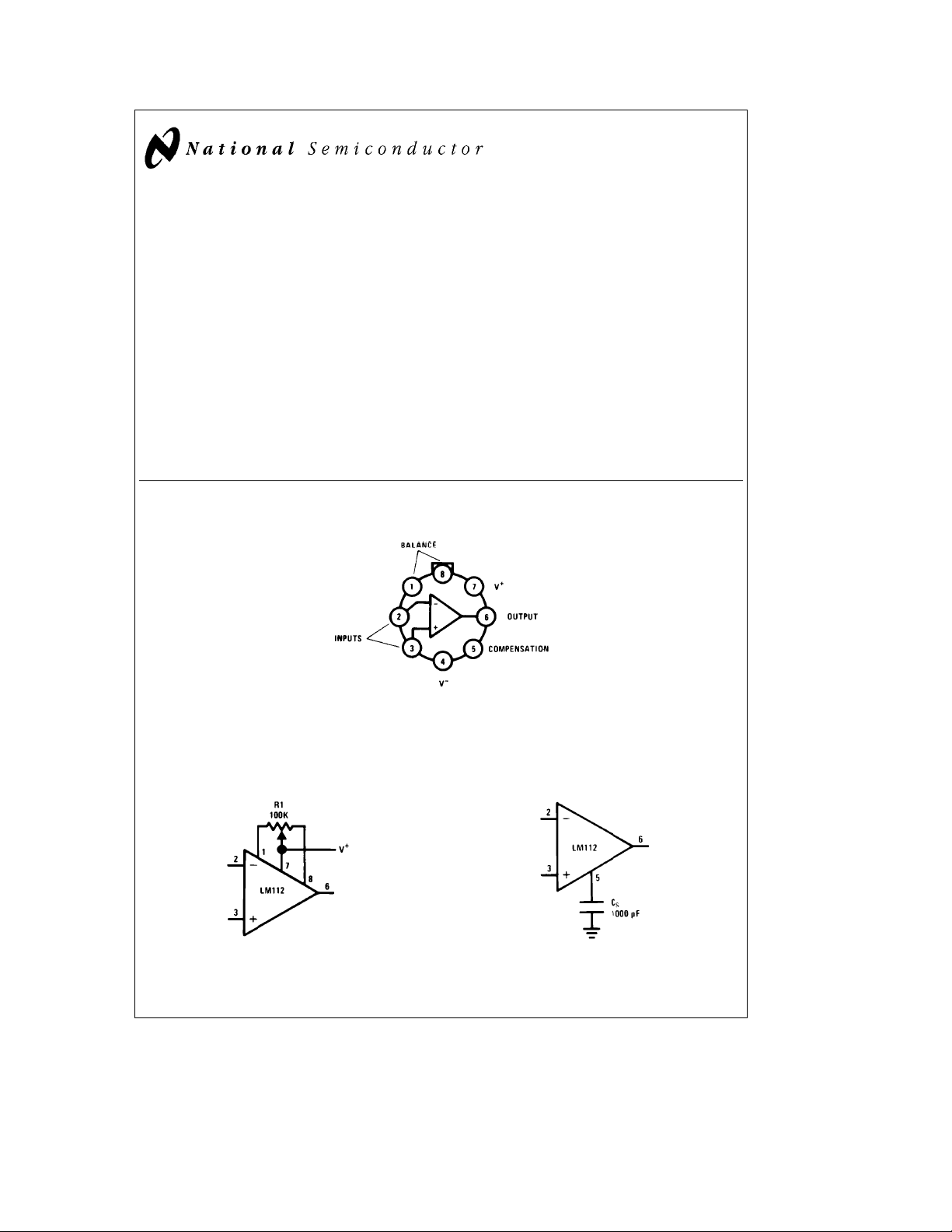
Connection Diagram
Metal Can Package
known to suffer catastrophic failure caused by short-duration overvoltage spikes on the supplies. Unlike other internally-compensated IC amplifiers, it is possible to overcompensate with an external capacitor to increase stability margin.
The LM212 is identical to the LM112, except that the LM212
has its performance guaranteed over a
temperature range instead of
2V to
LM312 is guaranteed over a 0
range.
Features
Y
Maximum input bias current of 3 nA over temperature
Y
Offset current less than 400 pA over temperature
Y
Low noise
Y
Guaranteed drift specifications
September 1992
b
b
Ctoa70§C temperature
§
25§Ctoa85§C
55§Ctoa125§C. The
LM112/LM212/LM312 Operational Amplifiers
Top View
Order Number LM112H, LM212H, LM312H or LM112H/883
See NS Package Number H08C
TL/H/7751– 4
Auxiliary Circuits
Offset Balancing
TL/H/7751– 2
C
1995 National Semiconductor Corporation RRD-B30M115/Printed in U. S. A.
TL/H/7751
Overcompensation for Greater Stability Margin
TL/H/7751– 3

Absolute Maximum Ratings
If Military/Aerospace specified devices are required, please contact the
National Semiconductor Sales Office/Distributors for availability and
specifications.
(Note 5)
LM112/LM212 LM312
Supply Voltage
g
20V
g
18V
Power Dissipation (Note 1) 500 mW 500 mW
Differential Input Current (Note 2)
Input Voltage (Note 3)
g
g
10 mA
15V
g
g
10 mA
15V
Output Short-Circuit Duration Continuous Continuous
Operating Temperature Range
LM112
LM212
Storage Temperature Range
b
55§Ctoa125§C0
b
25§Ctoa85§C
b
65§Ctoa150§Cb65§Ctoa150§C
Ctoa70§C
§
Lead Temperature (Soldering, 10 sec.) 300§C 300§C
ESD rating to be determined.
Electrical Characteristics (Note 4)
Parameter Conditions
Input Offset Voltage T
Input Offset Current T
Input Bias Current T
Input Resistance T
Supply Current T
Large Signal Voltage Gain T
e
25§C 0.7 2.0 2.0 7.5 mV
A
e
25§C 0.05 0.2 0.2 1 nA
A
e
25§C 0.8 2.0 1.5 7 nA
A
e
25§C30701040MX
A
e
25§C 0.3 0.6 0.3 0.8 mA
A
V
A
OUT
e
25§C, V
e
g
S
10V, R
e
g
15V
t
10 kX
L
Input Offset Voltage 3.0 10 mV
Average Temperature
Coefficient of Input 3.0 15 6.0 30 mV/§C
Offset Voltage
Input Offset Current 0.4 1.5 nA
Average Temperature
Coefficient of Input 0.5 2.5 2.0 10 pA/
Offset Current
Input Bias Current 3.0 10 nA
Supply Current T
Large Signal Voltage Gain V
Output Voltage Swing V
Input Voltage Range V
e
125§C 0.15 0.4 mA
A
e
g
15V, V
S
t
R
10 kX 25 15 V/mV
L
e
g
15V, R
S
e
g
15V
S
OUT
L
e
e
g
10 kX
10V
Common-Mode Rejection Ratio 85 100 80 100 dB
Supply Voltage Rejection Ratio 80 96 80 96 dB
Note 1: The maximum junction temperature of the LM112 is 150§C, LM212 is 100§C and LM312 is 85§C. For operating at elevated temperatures, devices in the H08
package must be derated based on a thermal resistance of 160
Note 2: The inputs are shunted with shunt diodes for overvoltage protection. Therefore, excessive current will flow if a differential input voltage in excess of 1V is
applied between the inputs unless some limiting resistance is used.
Note 3: For supply voltages less than
Note 4: These specifications apply for
s
a
CsT
0
§
Note 5: Refer to RETS112X for LM112H military specifications.
70§C (LM312) unless otherwise noted.
A
g
15V, the absolute maximum input voltage is equal to the supply voltage.
s
g
5VsV
S
C/W, junction to ambient, or 20§C/W, junction to case.
§
g
20V andb55§CsT
A
LM112/LM212 LM312
Min Typ Max Min Typ Max
50 300 25 300 V/mV
g
g
s
a
125§C (LM112),b25§CsT
13
13.5
g
14
g
13g14 V
g
14 V
s
a
85§C (LM212),g5VsV
A
Units
§
s
g
15V and
S
C
2
 Loading...