

NSC LM101AW-883, LM101AW-MLS, LM101AMW8, LM101AH-883, LM101AJ-883 Datasheet

LM101A/LM201A/LM301A
Operational Amplifiers
General Description
The LM101A series are general purpose operational amplifiers which feature improved performance over industry standards like the LM709. Advanced processing techniques
make possible an order of magnitude reduction in input currents, and a redesign of the biasing circuitry reduces the
temperature drift of input current.Improvedspecificationsinclude:
•
Offset voltage 3 mV maximum over temperature
(LM101A/LM201A)
•
Input current 100 nA maximum over temperature
(LM101A/LM201A)
•
Offset current 20 nA maximum over temperature
(LM101A/LM201A)
•
Guaranteed drift characteristics
•
Offsets guaranteed over entire common mode and supply voltage ranges
•
Slew rate of 10V/µs as a summing amplifier
This amplifier offers many features which make its appli-
cation nearly foolproof: overload protection on the input
and output, no latch-up when the common mode range is
exceeded, and freedom from oscillations and compensation with a single 30 pF capacitor. It has advantages over
internally compensated amplifiers in that the frequency
compensation can be tailored to the particular application. For example, in low frequency circuits it can be overcompensated for increased stability margin. Or the compensation can be optimized to give more than a factor of
ten improvement in high frequency performance for most
applications.
In addition, the device provides better accuracy and lower
noise in high impedance circuitry. The low input currents
also make it particularly well suited for long interval integrators or timers, sample and hold circuits and low frequency waveform generators. Further, replacing circuits
where matched transistor pairs buffer the inputs of conventional IC op amps, it can give lower offset voltage and
a drift at a lower cost.
The LM101A is guaranteed over a temperature range of
−55˚C to +125˚C, the LM201A from −25˚C to +85˚C, and
the LM301A from 0˚C to +70˚C.
Connection Diagrams (Top View)
Dual-In-Line Package
DS007752-4
Order Number LM101AJ, LM101J/883 (Note 1),
LM201AN or LM301AN
See NS Package Number J08A or N08E
Ceramic Flatpack Package
DS007752-40
Order Number LM101AW/883 or LM101W/883
See NS Package Number W10A
September 1999
LM101A/LM201A/LM301A Operational Amplifiers
© 1999 National Semiconductor Corporation DS007752 www.national.com

Connection Diagrams (Top View) (Continued)
Note 1: Available per JM38510/10103.
Metal Can Package
DS007752-2
Note: Pin 4 connected to case.
Order Number LM101AH, LM101AH/883 (Note 1),
LM201AH or LM301AH
See NS Package Number H08C
Dual-In-Line Package
DS007752-3
Order Number LM101AJ-14/883 (Note 1)
See NS Package Number J14A
www.national.com 2

Absolute Maximum Ratings (Note 2)
If Military/Aerospace specified devices are required, please contact the National Semiconductor Sales Office/
Distributors for availability and specifications.
LM101A/LM201A LM301A
Supply Voltage
±
22V
±
18V
Differential Input Voltage
±
30V
±
30V
Input Voltage (Note 3)
±
15V
±
15V
Output Short Circuit Duration (Note 4) Continuous Continuous
Operating Ambient Temp. Range −55˚C to +125˚C (LM101A) 0˚C to +70˚C
−25˚C to +85˚C (LM201A)
T
J
Max
H-Package 150˚C 100˚C
N-Package 150˚C 100˚C
J-Package 150˚C 100˚C
Power Dissipation at T
A
=
25˚C
H-Package (Still Air) 500 mW 300 mW
(400 LF/Min Air Flow) 1200 mW 700 mW
N-Package 900 mW 500 mW
J-Package 1000 mW 650 mW
Thermal Resistance (Typical) θ
jA
H-Package (Still Air) 165˚C/W 165˚C/W
(400 LF/Min Air Flow) 67˚C/W 67˚C/W
N Package 135˚C/W 135˚C/W
J-Package 110˚C/W 110˚CmW
(Typical) θ
jC
H-Package 25˚C/W 25˚C/W
Storage Temperature Range −65˚C to +150˚C −65˚C to +150˚C
Lead Temperature (Soldering, 10 sec.)
Metal Can or Ceramic 300˚C 300˚C
Plastic 260˚C 260˚C
ESD Tolerance (Note 7) 2000V 2000V
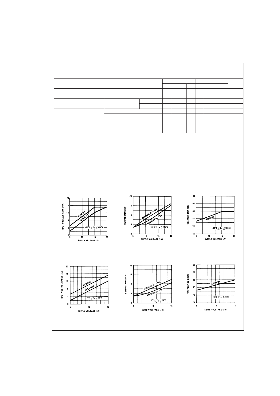
Electrical Characteristics (Note 5)
T
A
=
T
J
Parameter Conditions LM101A/LM201A LM301A Units
Min Typ Max Min Typ Max
Input Offset Voltage T
A
=
25˚C, R
S
≤ 50 kΩ 0.7 2.0 2.0 7.5 mV
Input Offset Current T
A
=
25˚C 1.5 10 3.0 50 nA
Input Bias Current T
A
=
25˚C 30 75 70 250 nA
Input Resistance T
A
=
25˚C 1.5 4.0 0.5 2.0 MΩ
Supply Current T
A
=
25˚C V
S
=
±
20V 1.8 3.0 mA
V
S
=
±
15V 1.8 3.0 mA
Large Signal Voltage Gain T
A
=
25˚C, V
S
=
±
15V 50 160 25 160 V/mV
V
OUT
=
±
10V, RL≥ 2kΩ
Input Offset Voltage R
S
≤ 50 kΩ 3.0 10 mV
Average Temperature Coefficient R
S
≤ 50 kΩ 3.0 15 6.0 30 µV/˚C
of Input Offset Voltage
Input Offset Current 20 70 nA
Average Temperature Coefficient 25˚C ≤ T
A
≤ T
MAX
0.01 0.1 0.01 0.3 nA/˚C
of Input Offset Current T
MIN
≤ TA≤ 25˚C 0.02 0.2 0.02 0.6 nA/˚C
Input Bias Current 0.1 0.3 µA
Supply Current T
A
=
T
MAX,VS
=
±
20V 1.2 2.5 mA
www.national.com3
Electrical Characteristics (Note 5) (Continued)
T
A
=
T
J
Parameter Conditions LM101A/LM201A LM301A Units
Min Typ Max Min Typ Max
Large Signal Voltage Gain V
S
=
±
15V, V
OUT
=
±
10V 25 15 V/mV
R
L
≥ 2k
Output Voltage Swing V
S
=
±
15V R
L
=
10 kΩ
±
12±14
±
12±14 V
R
L
=
2kΩ
±10±
13
±
10±13 V
Input Voltage Range V
S
=
±
20V
±
15 V
V
S
=
±
15V +15,
−13
±
12 +15,
−13
V
Common-Mode Rejection Ratio R
S
≤ 50 kΩ 80 96 70 90 dB
Supply Voltage Rejection Ratio R
S
≤ 50 kΩ 80 96 70 96 dB
Note 2: Absolute Maximum Ratings indicate limits beyond which damage to the device may occur.Operating ratings indicate for which the device is functional, but
do no guarantee specific performance limits. Electrical Characteristics state DC andAC electrical specifications under particular test conditions which guarantee specific limits. This assumes that the device is within the Operating Ratings. Specifications are not guaranteed for parameters where no limit is given, however,the typical
value is a good indication of device performance.
Note 3: For supply voltages less than
±
15V, the absolute maximum input voltage is equal to the supply voltage.
Note 4: Continuous short circuit is allowed for case temperatures to 125˚C and ambient temperatures to 75˚C for LM101A/LM201A, and 70˚C and 55˚C respectively
for LM301A.
Note 5: Unless otherwise specified, these specifications apply for C1=30 pF,
±
5V ≤ VS≤±20V and −55˚C ≤ TA≤ +125˚C (LM101A),±5V ≤ VS≤±20V and −25˚C
≤ T
A
≤ +85˚C (LM201A),±5V ≤ VS≤±15V and 0˚C ≤ TA≤ +70˚C (LM301A).
Note 6: Refer to RETS101AX for LM101A military specifications and RETS101X for LM101 military specifications.
Note 7: Human body model, 100 pF discharged through 1.5 kΩ.
Guaranteed Performance Characteristics LM101A/LM201A
Guaranteed Performance Characteristics LM301A
Input Voltage Range
DS007752-41
Output Swing
DS007752-42
Voltage Gain
DS007752-43
Input Voltage Range
DS007752-44
Output Swing
DS007752-45
Voltage Gain
DS007752-46
www.national.com 4

Typical Performance Characteristics
Supply Current
DS007752-47
Voltage Gain
DS007752-48
Maximum Power Dissipation
DS007752-49
Input Current,
LM101A/LM201A/LM301A
DS007752-50
Current Limiting
DS007752-51
Input Noise Voltage
DS007752-52
Input Noise Current
DS007752-53
Common Mode Rejection
DS007752-54
Power Supply Rejection
DS007752-55
www.national.com5

Typical Performance Characteristics (Continued)
Typical Performance Characteristics for Various Compensation Circuits
(Note 9)
Closed Loop Output
Impedance
DS007752-56
Single Pole Compensation
DS007752-8
CS=30pF
Two Pole Compensation
DS007752-12
CS=30pF
C2=10C1
Feedforward Compensation
DS007752-16
f
o
=
3 MHz
www.national.com 6
 Loading...