

© 2000 National Semiconductor Corporation www.national.com
Geode™ CS5530 I/O Companion Multi-Function South Bridge
April 2000
Geode™ CS5530 I/O Companion
Multi-Function South Bridge
General Description
The CS5530 I/O companion is designed to work in conjunction with the GXLV and GXm series processors; all
members of the National Semiconductor
®
Geode™ family
of products. Together the Geode processor and CS5530
provide a system-level solution well suited for the high
performance needs of a host of devices such as digital
set-top boxes and thin c lient devices. Due to the low
power consumption of a GXLV processor, this solution
satisfies the needs of battery powered devices such as
National’s WebPAD™ system, a Geode GXLV processor/CS5530 based design. Also, thermal design is eased
allowing forfanless system design.
The CS5530 I/O companion is a PCI-to-ISA bridge (South
Bridge), ACPI-compliant chipset that provides AT/ISA
style functionality. To those familiar with PC architecture
this enables a quicker understanding of the CS5530’s
architecture. The device contains state-of-the-art power
management that enables systems, especially battery
powered systems, to significantly reduce power consumption.
Audiois supported throughPCIbusmaster engines which
connect to an AC97 compatible codec such as the
National Semiconductor LM4548. If industry standard
audio is required, a combination of hardwareandsoftware
called Virtual System Architecture
®
(VSA™) technology is
provided.
The GXLV processor’sgraphics/video output is connected
to the CS5530. The CS5530 graphics/video support
includes a PLL that generates the DOTclockfor the GXLV
processor (where the graphics controlleris located), video
acceleration hardware, gamma RAM plus three DACs for
RGB output to CRT, and digital RGB that can be directly
connected to TFT panels or NTSC/PAL encoders. The
digital RGB output can also be connected to the National
Semiconductor CS9210 Graphics Companion (a DSTN
Controller) for DSTN panel support. The CS9210 is also a
member of the Geode product family.
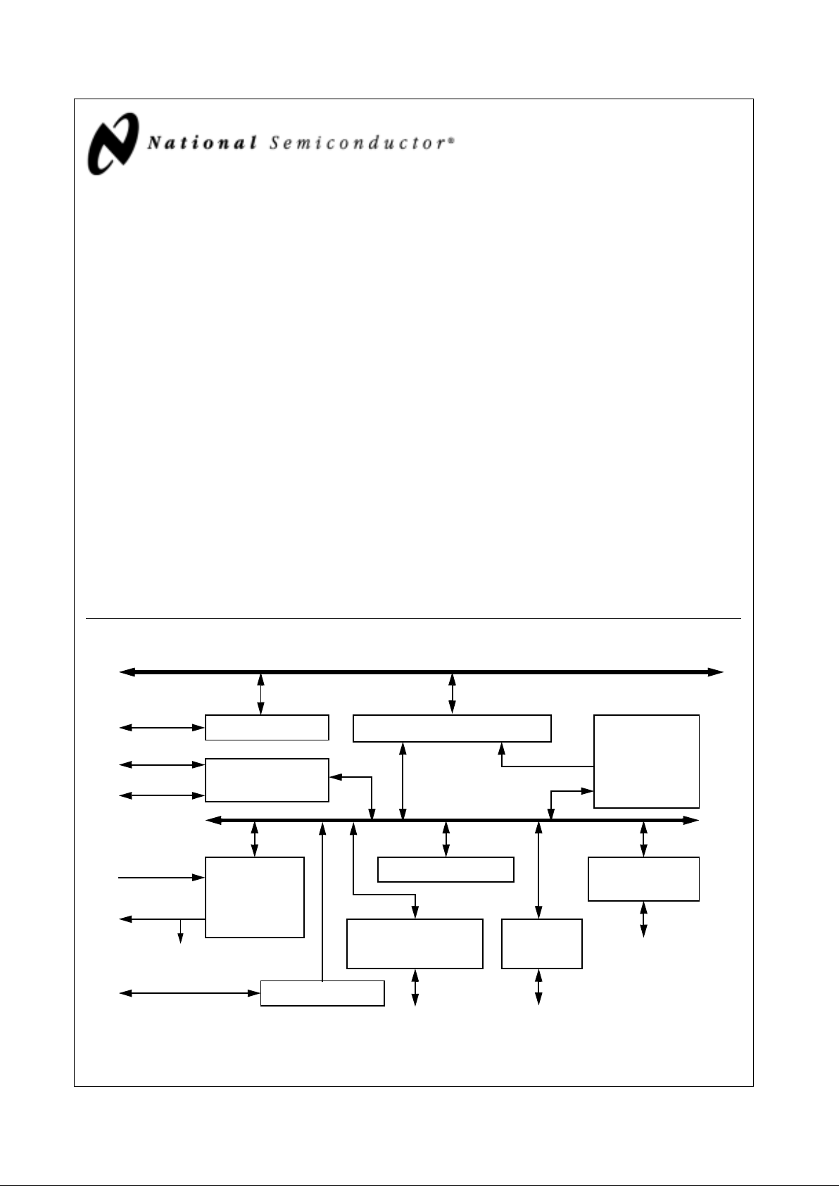
Geode™ CS5530 Internal Block Diagram
X-Bus
ISA Bus
PCI Bus
USB
PCI to X-Bus / X-Bus to PCI Bridge
PCI to USB Macro
Active Decode
Address Mapper
Audio/Codec/MPU
Interface
Pwr Mgmt, Traps,
Events, and Timers
IDE
Interface
Display Interface
MPEG, DOT Clock
CSC and SCL
RGB/FP Interface
AT Compatibility Logic
ISA Bus Interface
AT Ports, ISA Megacells
Display
PCI Configuration
Registers
Graphics
and Video
from CPU
X-Bus Arbiter
CS5530 Support
GPIOs
IDE
AC97 Codec
Ultra DMA/33
(e.g., LM4548)
Joystick / Game Port
Joystick
PC97317 SIO
GPCS
Geode™ CS9210
Graphics Companion
National Semiconductor and Virtual System Architecture are registered trademarks of National Semiconductor Cor poration.
Geode, VSA, and WebPAD are trademarks of National Semiconductor Corporation.
For a complete listing of National Semiconductor trademarks, please visit www.national.com/trademarks.
www.national.com 2 Revision 4.1
Geode™ CS5530
Two bus mastering IDE controllers are included for support of up to four ATA-compliant devices. A two-port Universal Serial Bus (USB) provides high speed, Plug & Play
expansion for a variety of consumer peripheral devices
such as a keyboard, mouse, printer, and digital cameras.
If additional functions are required, such as real-time
clock, floppy disk, PS2 keyboard, and PS2 mouse, a
SuperI/O (e.g., National PC97317) can be easily connected to the CS5530.
Features
General Features
Designed for use with the GXLV and GXm Geode
series processors
352-Terminal TapeBall Gr id Array(TBGA) package
3.3V or 5.0V PCI bus compatible
5.0V tolerant I/O interfaces
3.3V core
PCI-to-ISA Bridge
PCI 2.1 compliant
Supports PCI initiator-to-ISA and ISA master-to-PCI
cycle translations
PCI master for audio I/O and IDE controllers
Subtractive agent for unclaimed transactions
PCI-to-ISA interrupt mapper/translator
AT Compatibility
Two 8259A-equivalent interrupt controllers
8254-equivalent timer
Two 8237-equivalent DMA controllers
Boot ROM and keyboard chip select
ExtendedROMto16MB
Bus Mastering IDE Controllers
Two controllers with support for up to four IDE devices
Independent timing for master and slave devices for
both channels
PCI bus master burst reads and writes
Ultra DMA/33 (ATA-4)support
Multiword DMA support
Programmed I/O (PIO) Modes 0-4 support
Power Management
Intelligent system controller supports multiple power
management standards:
— Full ACPI and Legacy (APM) support
— Directly manages all GXLV and GXmprocessor
power states (including automatic Suspend modulation for optimal performance/thermal balancing)
I/O traps and idle timersfor peripheral power
management
Up to eight GPIOs for system control:
— All eight are configurable as external wakeupevents
Dedicated inputs for keyboard and mousewakeup
events
XpressAUDIO
Provides "back-end" hardware support via six buffered
PCI bus masters
AC97 codec interface:
— Specification Revision 1.3, 2.0, and 2.1 compliant
interface.Note that the codec (e.g., LM4548) must
have SRC (sample rate conversion) suppor t
Display Subsystem Extensions
Complements the GXLV and GXm processor’s
graphics and video capabilities:
— Three independent line buffers for accelerating
video data streams
— Handles asynchronous video and graphics data
streams concurrently from the processor
— YUV to RGB conversion hardware
— Arbitrary X & Y interpolative scaling
— Color keying for graphics/video overlay
VDACs/Displayinterface:
— Three integrated D ACs
— Gamma RAM:
– Provides gamma correction for graphics data
streams
– Provides brightness/contrast correction for video
data streams
— Integrated DOT clock generator
— Digital RGB interface drivesTFT panels or standard
NTSC/PAL encoders
Universal Serial Bus
Two independent USB interfaces:
— Open Host Controller Interface (OpenHCI)
specificationcompliant
— Second generation proven core design

Revision 4.1 3 www.national.com
Table of Contents
Geode™ CS5530
1.0 ArchitectureOverview..............................................6
1.1 PCIBUSINTERFACE ......................................................6
1.2 ISABUSINTERFACE ......................................................7
1.3 ATCOMPATIBILITYLOGIC..................................................7
1.3.1 DMAController.....................................................7
1.3.2 ProgrammableIntervalTimer..........................................7
1.3.3 ProgrammableInterruptController......................................7
1.4 IDECONTROLLERS .......................................................7
1.5 POWERMANAGEMENT ....................................................8
1.5.1 GPIOInterface .....................................................8
1.6 XPRESSAUDIO ...........................................................8
1.6.1 AC97CodecInterface ...............................................8
1.6.2 VSATechnologySupportHardware.....................................8
1.7 DISPLAYSUBSYSTEMEXTENSIONS.........................................9
1.8 CLOCKGENERATION ....................................................10
1.9 UNIVERSALSERIALBUS..................................................10
1.10 PROCESSORSUPPORT ..................................................11
2.0 SignalDefinitions.................................................12
2.1 PINASSIGNMENTS ......................................................13
2.2 SIGNALDESCRIPTIONS ..................................................22
2.2.1 ResetInterface....................................................22
2.2.2 ClockInterface ....................................................22
2.2.3 CPUInterface.....................................................23
2.2.4 PCIInterface .....................................................24
2.2.5 ISABusInterface ..................................................27
2.2.6 ROMInterface ....................................................30
2.2.7 IDEInterface .....................................................31
2.2.8 USBInterface.....................................................32
2.2.9 GamePortandGeneralPurposeI/OInterface ...........................32
2.2.10 AudioInterface ....................................................33
2.2.11 DisplayInterface...................................................34
2.2.12 DCLKPLL .......................................................38
2.2.13 Power,Ground,andReserved........................................39
2.2.14 InternalTestandMeasurement .......................................39
3.0 Functional Description . . . . . . . . . . . . . . . . . . . . . . . . . . . . . . . . . . . . . . . . . . . . 40
3.1 PROCESSORINTERFACE .................................................41
3.1.1 DisplaySubsystemConnections ......................................42
3.1.2 PSERIALPinInterface..............................................44
3.1.2.1 VideoRetraceInterrupt .............................................44
3.2 PCIBUSINTERFACE .....................................................45
3.2.1 PCIInitiator ......................................................45
3.2.2 PCITarget .......................................................46
3.2.3 SpecialBusCycles–Shutdown/Halt ....................................47
3.2.4 PCIBusParity ....................................................47
3.2.5 PCIInterruptRoutingSupport ........................................48
3.2.6 DelayedTransactions ...............................................48

www.national.com 4 Revision 4.1
Table of Contents (Continued)
Geode™ CS5530
3.3 RESETSANDCLOCKS....................................................49
3.3.1 Resets ..........................................................49
3.3.2 ISAClock ........................................................49
3.3.3 DOTClock .......................................................50
3.3.3.1 DCLKProgramming................................................51
3.4 POWERMANAGEMENT ...................................................54
3.4.1 APMSupport .....................................................54
3.4.2 CPUPowerManagement............................................55
3.4.2.1 SuspendModulation ...............................................55
3.4.2.2 3VoltSuspend....................................................58
3.4.2.3 Save-To-Disk .....................................................59
3.4.3 PeripheralPowerManagement .......................................60
3.4.3.1 DeviceIdleTimersandTraps ........................................60
3.4.3.2 GeneralPurposeTimers ............................................70
3.4.3.3 ACPITimerRegister ...............................................72
3.4.3.4 GeneralPurposeI/OPins ...........................................73
3.4.3.5 PowerManagementSMIStatusReportingRegisters......................75
3.4.3.6 Device Power Management Register Programming Summary . . . . . . . . . . . . . . . 82
3.5 PC/ATCOMPATIBILITYLOGIC..............................................84
3.5.1 ISASubtractiveDecode .............................................84
3.5.2 ISABusInterface ..................................................85
3.5.2.1 DelayedPCITransactions ...........................................86
3.5.2.2 LimitedISAandISAMasterModes....................................87
3.5.2.3 ISABusDataSteering..............................................89
3.5.2.4 I/ORecoveryDelays ...............................................89
3.5.2.5 ISADMA ........................................................90
3.5.3 ROMInterface ....................................................91
3.5.4 Megacells ........................................................91
3.5.4.1 DirectMemoryAccess(DMA)........................................92
3.5.4.2 ProgrammableIntervalTimer ........................................94
3.5.4.3 ProgrammableInterruptController ....................................95
3.5.4.4 PCICompatibleInterrupts ...........................................98
3.5.5 I/OPorts092hand061hSystemControl...............................100
3.5.5.1 I/OPort092hSystemControl .......................................101
3.5.5.2 I/OPort061hSystemControl .......................................101
3.5.5.3 SMIGenerationforNMI............................................101
3.5.6 KeyboardInterfaceFunction ........................................102
3.5.6.1 FastKeyboardGateAddress20andCPUReset ........................103
3.5.7 ExternalReal-TimeClockInterface ...................................104
3.6 IDECONTROLLER ......................................................105
3.6.1 IDEInterfaceSignals ..............................................105
3.6.2 IDEConfigurationRegisters.........................................106
3.6.2.1 PIOMode ......................................................106
3.6.2.2 BusMasterMode ................................................108
3.6.2.3 UltraDMA/33Mode ...............................................111
3.7 XPRESSAUDIO .........................................................113
3.7.1 SubsystemDataTransportHardware .................................113
3.7.1.1 AudioBusMasters................................................113
3.7.1.2 PhysicalRegionDescriptorTableAddress .............................116
3.7.1.3 PhysicalRegionDescriptorFormat ...................................116
3.7.1.4 ProgrammingModel ..............................................117
3.7.1.5 AC97CodecInterface .............................................118
3.7.2 VSATechnologySupportHardware...................................120
3.7.2.1 VSATechnology .................................................120
3.7.2.2 AudioSMIRelatedRegisters........................................120
3.7.2.3 IRQConfigurationRegisters ........................................126

Revision 4.1 5 www.national.com
Table of Contents (Continued)
Geode™ CS5530
3.8 DISPLAYSUBSYSTEMEXTENSIONS.......................................128
3.8.1 VideoInterfaceConfigurationRegisters................................128
3.8.2 VideoAccelerator.................................................129
3.8.2.1 LineBuffers .....................................................129
3.8.2.2 VideoPortProtocol ...............................................129
3.8.2.3 VideoFormat....................................................130
3.8.2.4 XandYScaler/Filter .............................................131
3.8.2.5 Color-Space-Converter ............................................131
3.8.3 VideoOverlay....................................................132
3.8.4 GammaRAM ....................................................133
3.8.5 DisplayInterface..................................................134
3.8.5.1 VideoDACs .....................................................134
3.8.5.2 VESA DDC2B / DPMS . . . . . . . . . . . . . . . . . . . . . . . . . . . . . . . . . . . . . . . . . . . . 134
3.8.5.3 FlatPanelSupport................................................134
3.9 UNIVERSALSERIALBUSSUPPORT .......................................135
3.9.1 USBPCIController ...............................................135
3.9.2 USBHostController...............................................136
3.9.3 USB Power Management ...........................................136
4.0 RegisterDescriptions ............................................137
4.1 PCICONFIGURATIONSPACEANDACCESSMETHODS .......................138
4.2 REGISTERSUMMARY ...................................................139
4.3 CHIPSETREGISTERSPACE ..............................................149
4.3.1 BridgeConfigurationRegisters-Function0 ............................149
4.3.2 SMIStatusandACPITimerRegisters-Function1.......................179
4.3.3 IDEControllerRegisters-Function2 .................................184
4.3.4 XpressAUDIORegisters-Function3..................................188
4.3.5 VideoControllerRegisters-Function4 ................................199
4.4 USBCONTROLLERREGISTERS-PCIUSB ..................................206
4.5 ISALEGACYI/OREGISTERSPACE ........................................208
4.6 V-ACPII/OREGISTERSPACE .............................................217
5.0 ElectricalSpecifications ..........................................224
5.1 TESTMODES...........................................................224
5.1.1 NandTreeMode..................................................225
5.2 ELECTRICALCONNECTIONS .............................................227
5.2.1 Pull-UpResistors .................................................227
5.2.2 UnusedInputPins ................................................227
5.2.3 NC-DesignatedPins...............................................227
5.2.4 Power/GroundConnectionsandDecoupling ............................227
5.3 ABSOLUTEMAXIMUMRATINGS...........................................227
5.4 RECOMMENDEDOPERATINGCONDITIONS.................................227
5.5 DCCHARACTERISTICS .................................................228
5.6 ACCHARACTERISTICS ..................................................230
5.7 VIDEOCHARACTERISTICS ...............................................234
6.0 MechanicalSpecifications ........................................238
Appendix A Support Documentation . . . . . . . . . . . . . . . . . . . . . . . . . . . . . . . . . . . 240
A.1 REVISIONHISTORY .....................................................240
www.national.com 6 Revision 4.1
Geode™ CS5530
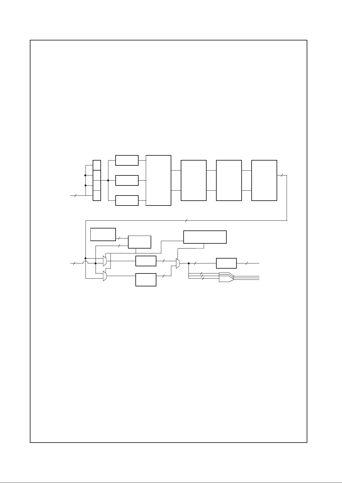
1.0 Architecture Overview
The Geode CS5530 can be described as providing the
functional blocks shown in Figure 1-1.
• PCI bus master/slave interface
• ISA bus interface
• AT compatibility logic
• IDE controllers
• Power management
-GPIOinterfaces
- Traps, Events, Timers
• Joystick/Game Port interface
• Virtual audio support hardware
• Videodisplay, whichincludes MPEG accelerator,
RAMDAC, and videoports
•USBcontrollers
For CPU interface connection refer to Figure 1-5 on page
11.
1.1 PCI BUS INTERFACE
The CS5530 provides a PCI bus interface that is both a
slave for PCI cycles initiated by the CPU or other PCI
master devices, and a non-preemptable master for DMA
transfercycles. The chip also isa standard PCI master for
the IDE controllers and audio I/O logic. The CS5530 supports positive decode for configurable memory and I/O
regions and implements a subtractive decode option for
unclaimed PCI accesses. The CS5530 also generates
address and data parity and performs parity checking.
The CS5530 does not include the PCI bus arbiter, it is
locatedintheprocessor.
Configuration registers are accessed through the PCI
interface using the PCI Bus Type 1 configuration mechanism as described in the PCI 2.1Specification.
Figure 1-1. Internal Block Diagram
X-Bus
ISA B us
PCI Bus
USB
PCI to X-Bus / X-Bus to PCI Bridge
PCI to USB Macro
Active Decode
Address Mapper
Audio/Codec/MPU
Interface
Pwr Mgmt, Traps,
Events, and Timers
IDE
Interface
Display Interface
MPEG, DOT Clock
CSC and SCL
RGB/FP Interface
AT Compatibility Logic
ISA Bus Interface
AT Ports, ISA Megacells
Display
PCI Configuration
Registers
Graphics
and Video
from CPU
X-Bus Arbiter
CS5530 Support
GPIOs
IDE
AC97 Codec
Ultra DMA/33
(e.g., LM4548)
Joystick / Game Port
Joystick
PC97317 SIO
GPCS
Geode™ CS9210
Graphics Companion

Revision 4.1 7 www.national.com
Architecture Overview (Continued)
Geode™ CS5530
1.2 ISA BUS INTERFACE
The CS5530 provides an ISA bus interface for unclaimed
memory and I/O cycles on PCI. The CS5530 is the default
subtractive decoding agent and forwards all unclaimed
memory and I/O cycles to the ISA interface; however, the
CS5530 may be configured to ignore either I/O, memory
or all unclaimed cycles (subtractive decode disabled).
The CS5530 supports two modes on the ISA interface.
The default mode, Limited ISA Mode, supports the full
memory and I/O address range without ISA mastering.
The address and data buses are multiplexed together,
requiring an external latch to latch the lower 16 bits of
address of the ISA cycle. The signal SA_LATCH is generated when the data on the SA/SD bus is a valid address.
Additionally, the upper four address bits, SA[23:20] are
multiplexed on GPIO[7:4].
The second mode, ISA Master Mode, supports ISA bus
masters and requires no external circuitry. When the
CS5530 is placed in ISA Master Mode, a large number of
pins are redefined. In this mode of operation the CS5530
cannot support TFT flat panels or TV controllers, since
most of the signals used to support these functions have
been redefined. This mode is required if ISA slots or ISA
masters are used. ISA master cycles are only passed to
the PCI bus i f they access memory. I/O accesses are left
to complete on the ISAbus.
For further information regarding mode selection and
operational details refer to Section 3.5.2.2 “Limited ISA
and ISA Master Modes” on page 87.
1.3 AT COMPATIBILITY LOGIC
The CS5530 integrates:
• Two 8237-equivalent DMA c ontrollers withfull 32-bit
addressing
• Two 8259-equivalent interrupt controllers providing 13
individually programmable external interrupts
• An 8254-equivalent timer for refresh, timer, and
speaker logic
• NMI control and generation for PCI system errors and
all parity errors
• Support for standard AT keyboard controllers
• Positive decode for the AT I/O register space
• Reset control
1.3.1 DMA Controller
The CS5530 supports the industry standard DMA architecture using two 8237-compatible DMA controllers in
cascaded configuration. CS5530-supported DMA functions include:
• Standard seven-channel DMA support
• 32-bit address range support via high page registers
• IOCHRDY extended cycles for compatible timing
transfers
• ISA bus master device support using cascade mode
1.3.2 Programmable Interval Timer
The CS5530 contains an 8254-equivalent programmable
interval timer. This device has three timers, each with an
input frequency of 1.193 MHz.
1.3.3 Programmable Interrupt Controller
The CS5530 contains two 8259-equivalent programmable
interrupt controllers, with eight interrupt request lines
each, for a total of 16 interrupts. The two controllers are
cascaded internally, and two of the interrupt request
inputs are connected to the internal circuitry. This allows a
total of 13 externally available interrupt requests.
Each CS5530 IRQ signal can be individually selected as
edge- or level-sensitive. The PCI interrupt signals are
routed internally to the PIC IRQs.
1.4 IDE CONTROLLERS
The CS5530 integrates two PCI bus mastering, ATA-4
compatible IDE controllers. These controllers support
UltraDMA/33(enabledinMicrosoftWindows95andWindows NT by using a driver provided by National Semiconductor), Multiword DMA and Programmed I/O (PIO)
modes. Two devices are supported on each controller.
The data-transfer speed for each device on each controller can be independently programmed. This allows highspeed IDE peripherals to coexist on the same channel as
lower speed devices. Faster devices must be ATA-4 compatible.
www.national.com 8 Revision 4.1
Architecture Overview (Continued)
Geode™ CS5530
1.5 POWER MANAGEMENT
The CS5530 integrates advanced power management
featuresincluding:
• Idle timers for common system peripherals
• Addresstrap registers for programmable address
ranges for I/O or memory accesses
• Up to eight programmable GPIOs
• Clock throttling with automatic speedup for the CPU
clock
• SoftwareCPU stop clock
• Zero Volt Suspend/Resume with peripheral shadow
registers
• Dedicated serial bus to/from the GXLV processor
providing CPU power management status
TheCS5530isanACPI(AdvancedControlandPower
Interface)compliant chipset. An ACPI compliant system is
one whose underlying BIOS, device drivers, chipset and
peripherals conform to revision 1.0 or newer of the ACPI
specification. The “Fixed Feature” and “General Purpose”
registers are virtual. They are emulated by the SMI handling code rather than existing in physical hardware. To
the ACPI compliant operating system, the SMI-base virtualization is transparent; however, to eliminate unnecessary latencies, the ACPI timer exists in physical hardware.
The CS5530 V-ACPI (Virtual ACPI) solution provides the
following support:
• CPU States — C1, C2
• Sleep States — S1, S2, S4, S4BIOS, S5
• EmbeddedController (Optional) — SCI and SWI event
inputs.
• GeneralPurpose Events
— Fully programmable GPE0
Event Block registers.
1.5.1 GPIO Interface
Eight GPIO pins are provided for general usage in the
system. GPIO[3:0] are dedicated pins and can be configured as inputs or outputs. GPIO[7:4] can be configured as
the upper addresses of the ISA bus, SA[23:20]. All GPIOs
can also be configured to generate an SMI on input edge
transitions.
1.6 XPRESSAUDIO
XpressAUDIO i n the CS5530 offers a combined hardware/software support solution to meet industry standard
audio requirements. XpressAUDIO uses VSA technology
along with additional hardware features to provide the
necessary support for industry standard 16-bit stereo synthesis and OPL3 emulation.
The hardware portion of the XpressAUDIO subsystem
can broadly be divided into two categories. Hardware for:
• Transporting streaming audio data to/fromthe system
memoryandanAC97codec.
• VSA technology suppor t.
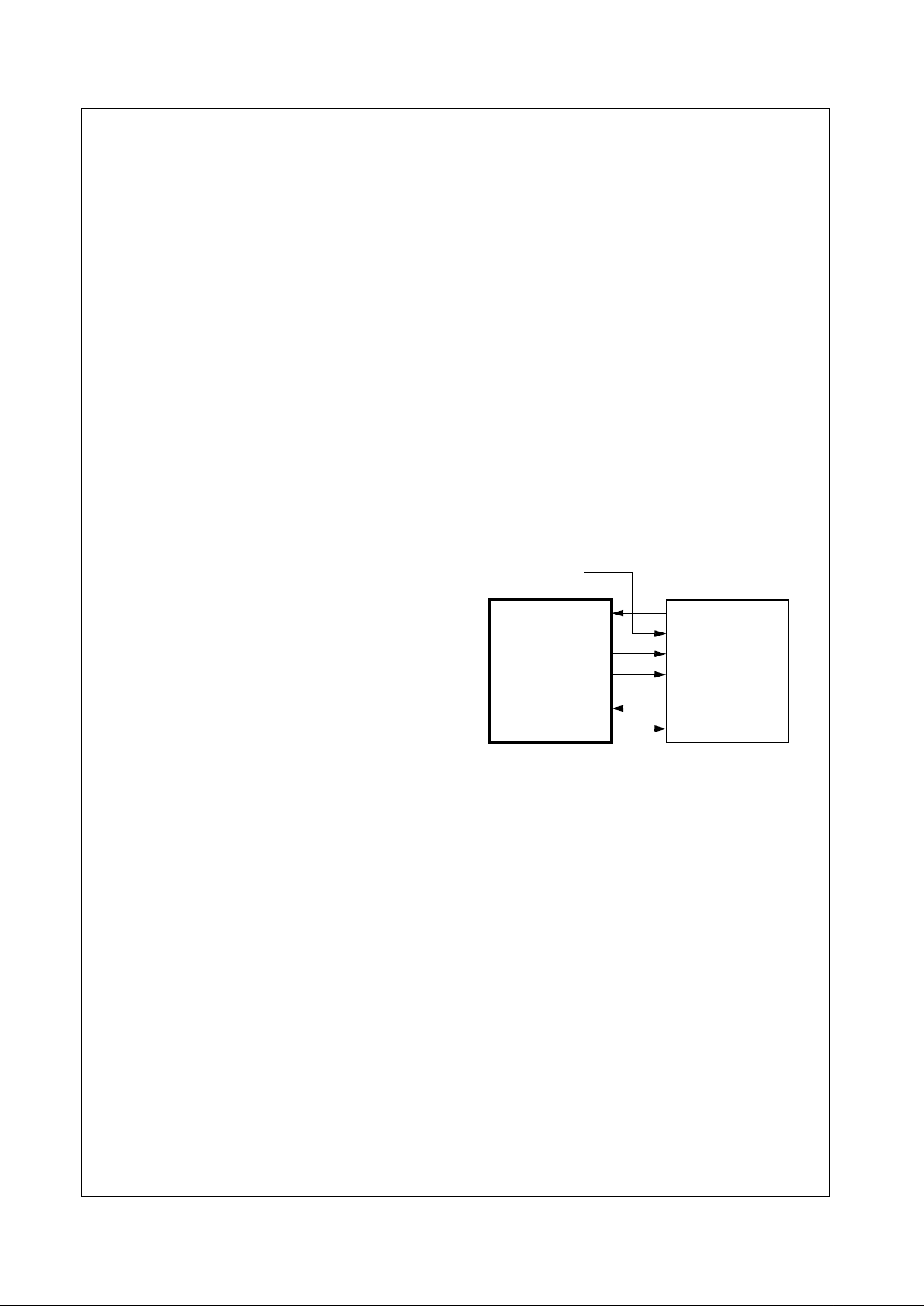
1.6.1 AC97 Codec Interface
The CS5530 provides an AC97 Specification Revision
1.3, 2.0, and 2.1 compatible interface. Any AC97 codec
which supports an independent input and output sample
rate conversion interface (e.g., National Semiconductor
LM4548) can be used with the CS5530. This type of
codec will allow for a design which meets the requirements for PC97 and PC98-compliant audio as defined by
Microsoft Corporation. Figure 1-2 shows the codec and
CS5530 signal connections. For specifics on the serial
interface, refer to the appropriate codec manufacturer’s
data sheet.
Low latency audio I/O is accomplished by a buffered PCI
bus mastering controller.
Figure 1-2. AC97 Codec Signal Connections
1.6.2 VSA Technology Support Hardware
The CS5530 I/O companion incorporates the required
hardware in order to support VSA technology for the capture and playback of audio using an external codec. This
eliminates much of the hardware traditionally associated
with industry standard audio functions.
XpressAUDIO software provides 16-bit compatible sound.
This software is available to OEMs for incorporation into
the system BIOS ROM.
BITCLK
PC_BEEP
SDAT_I
SDAT_O
PC_BEEP
SDATA_IN
SDATA_OUT
AC97
Geode™
BIT_CLK
24.576 MHz
SYNC SYNC
Codec
External Source
CS5530
Revision 4.1 9 www.national.com
Architecture Overview (Continued)
Geode™ CS5530
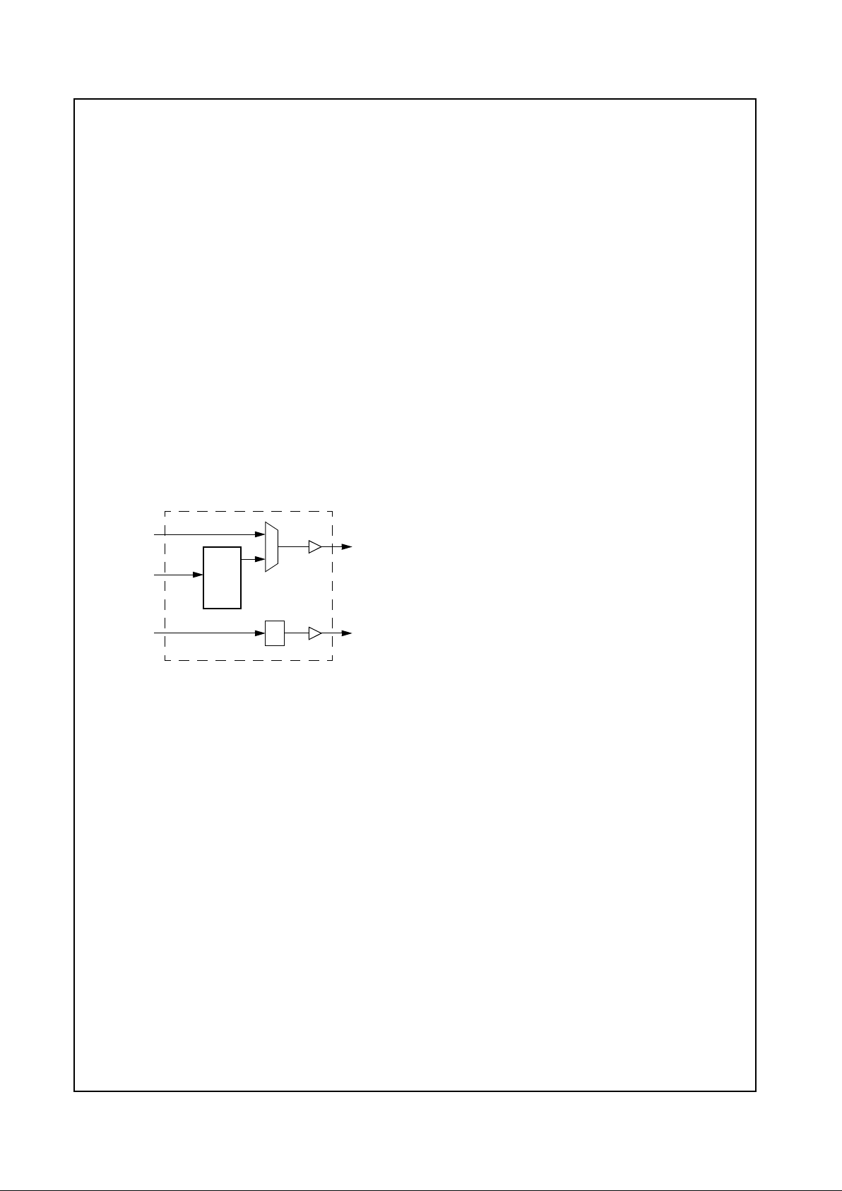
1.7 DISPLAY SUBSYSTEM EXTENSIONS
The CS5530 incorporates extensions to theGXLV processor’s display subsystem. These include:
• Video Accelerator
- Buffers and formats input YUV video data from
processor
- 8-bit interface to the GXLV processor
- X & Y scaler withbilinear filter
- Color space converter (YUV to RGB)
• VideoOverlay Logic
-Colorkey
- Data switch for graphics and video data
•GammaRAM
- Brightness and contrastcontrol
• Display Interface
- Integrated RGB Video DACs
- VESA DDC2B/DPMS support
- Flat panel interface
Figure 1-3 shows the data path of the display subsystem
extensions.
Figure 1-3. Display Subsystem Extensions, 8-Bit Interface
VID_DATA[7:0]
8
Input
Buffer 0
(3x360x32 bit)
Buffer 1
Buffer 2
Formatter
/
Scaler
Vertical
Filter
Horizontal
Filter
Color
Space
Converter
Formatter
24
Color Key
Color
Compare
24
PIXEL[23:0]
Bypass
Gamma
RAM
24
Video
Dither
24
8each
DAC
RGB to CRT
FP_DATA
18
24
24
Enable Gamma
Correction Register
24
24
Register
www.national.com 10 Revision 4.1
Architecture Overview (Continued)
Geode™ CS5530
1.8 CLOCK GENERATION
In a CS5530/GXLV processor-based system, the CS5530
generates only the video DOT clock (DCLK) for the CPU
and the ISA clock. All other clocks are generated by an
external clock chip.
The ISACLK is created by dividing the PCICLK. For ISA
compatibility, the ISACLK nominally runs at 8.33 MHz or
less. The ISACLK dividers are programmed via F0 Index
50h[2:0].
DCLK is generated from the 14.31818 MHz input
(CLK_14MHZ). A combination of a phase locked loop
(PLL), linear feedback shift register (LFSR) and divisors
are used to generate the desired frequencies for the
DCLK. The divisors and LFSR are configurable through
the F4BAR+Memory Offset 24h. For applications that do
not use the GXLV processor’s video, this is an available
clock for general purpose use.
Figure 1-4 shows a block diagram for clock generation
within the CS5530.
Figure 1-4. CS5530 Clock Generation
1.9 UNIVERSAL SERIAL BUS
The CS5530 provides two complete, independent USB
ports. Each port has a Data "–" and a Data "+" pin.
The USB controller is a compliant Open Host Controller
Interface (OpenHCI). The OpenHCI specification provides
a register-level description for a host controller, as well as
a common industry hardware/software interface and drivers (see OpenHCI Specification, Revision 1.0, for description).
DCLK
DCLK
PLL
÷N
TVCLK
CLK_14MHZ
ISACLK
PCICLK
M
U
X
Revision 4.1 11 www.national.com
Architecture Overview (Continued)
Geode™ CS5530
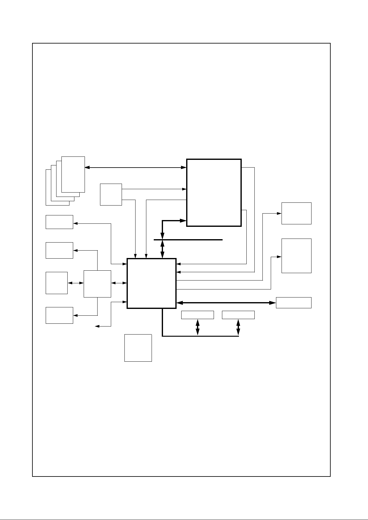
1.10 PROCESSOR SUPPORT
The traditional south bridge functionality included in the
CS5530 I/O companion chip has been designed to support the GXLV processor. When combined with the GXLV
processor, the CS5530 provides a bridge which supports
a standard ISA bus and system ROM. As part of the video
subsystem, the CS5530 provides MPEG video acceleration and a digital RGB interface, to allowdirect connection
to TFT LCD panels. This chip also integrates a gamma
RAM and three DACs, allowing for direct connection of a
CRT monitor. Figure 1-5 shows a typical system block diagram.
For detailed information regarding processor signal connections refer to Section 3.1 “Processor Interface” on
page 41.
Figure 1-5. System Block Diagram
YUV Port
(Video)
RGB Port
PCI Interface
Memory
Memory Data Bus
PCI Bus
Geode™ CS5530
I/O Companion
Graphics Data
Video Data
Analog RGB
Digital RGB
CRT
TFT
Flat Panel
USB
(2 Ports)
AC97
Codec
Speakers
CD
ROM
Audio
Microphone
GPIOs
Port
(Graphics)
Geode™ GXLV
IDE Devices
SuperI/O BIOS
ISA Bus
Ultra DMA/33 IDE Bus
Memory
Serial
Packet
DC-DC
&
Battery
Clocks
or TV
NTSC/PAL
Encoder
Processor
www.national.com 12 Revision 4.1
Geode™ CS5530
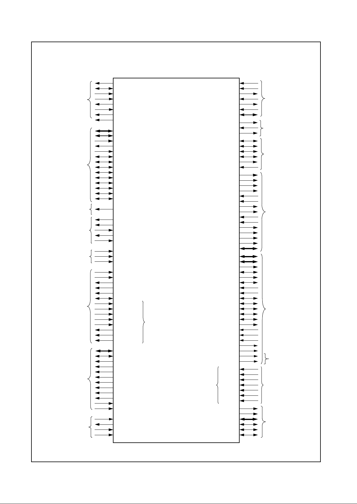
2.0 Signal Definitions
This section defines the signals and describes the external interface of the Geode CS5530. Figure 2-1 shows the
pins organized by their functional groupings (internal test
and electrical pins are not shown).
Figure 2-1. CS5530 Signal Groups
AD[31:0]
C/BE[3:0]#
PAR
HOLD_REQ#
FRAME#
TRDY#
STOP#
LOCK#
DEVSEL#
REQ#
GNT#
SERR#
INTA#-INTD#
IRQ13
INTR
SMI#
IDE_DACK1#
IDE_IORDY0
ROM Interface
PCI Bus
CPU Interface
IDE Controller
PSERIAL
SUSP#
SUSPA#
KBROMCS#
IRDY#
PERR#
SUSP_3V
IDE_IOW1#
IDE_IOW0#
IDE_IOR0#
IDE_IOR1#
Geode™ CS5530
IDE_DATA[15:0]
IDE_ADDR[2:0]
IDE_RST#
IDE_CS0#
IDE_CS1#
IDE_DREQ1
IDE_DACK0#
IDE_DREQ0
IDE_IORDY1
TVCLK
DCLK
PCICLK
ISACLK
Clocks
CLK_32K
CLK14_MHZ
Reset
PCI_RST#
POR#
CPU_RST
USBCLK
D+_PORT1
D–_PORT1
D+_PORT2
D–_PORT2
USB
POWER_EN
OVER_CUR#
SDATA_OUT
SDATA_IN
SYNC
BIT_CLK
PC_BEEP
Audio Interface
I/O Companion
VREF
EXTVREFIN
PCLK
IOUTG
IOUTB
AVSS1-5
IOUTR
AVDD1-3
HSYNC_OUT
HSYNC
VSYNC
PIXEL[23:0]
FP_DATA17 (MASTER#)
FP_CLK (No Function)
Display: Pixel
Display: CRT
ENA_DISP
VSYNC_OUT
DDC_SCL
DDC_SDA
FP_HSYNC_OUT (SMEMW#)
FP_CLK_EVEN (No Function)
FP_VSYNC_OUT (SMEMR#)
IREF
FP_DISP_ENA_OUT (No Function)
FP_ENA_VDD(No Function)
FP_ENA_BKL (No Function)
FP_HSYNC(No Function)
FP_VSYNC(No Function)
Analog
Display: MPEG
PLLDVD
PLLVAA
PLLRO
PLLLP
PLLAGS
DCLKPLL
Analog
Port
PLLAGD
PLLDGN
VID_RDY
VID_VAL
VID_CLK
VID_DATA[7:0]
SA[19:16]
(SA_DIR) SA_LATCH
SBHE#
BALE
IOCHRDY
ZEROWS#
IOR#
IOW#
MEMCS16#
MEMR#
MEMW#
AEN
DRQ[7:5], [3:0]
DACK#[7:5], [3:0]
TC
IRQ[15:14], [12:9], [7:3], 1
ISA Bus
IRQ8#
IOCS16#
(SD[15:0]) SA[15:0]/SD[15:0]
GPCS#
GPORT_CS#
(SA[23:20]) GPIO[7:4]/SA[23:20]
GPIO[3:2]
GPIO1/SDATA_IN2
GPIO0
Game Port/
GPIO
SMEMW#/RTCCS#
SMEMR#/RTCALE
FP_DATA16(SA_OE#)
FP_DATA[15:0] (SA[15:0])
External RTC
Display: TFT/TV
Note: Pins that change
function when ISA Master
mode is invoked are represented with the ISA Master Mode function signal
name in parenthesis.

Revision 4.1 13 www.national.com
Signal Definitions (Continued)
Geode™ CS5530
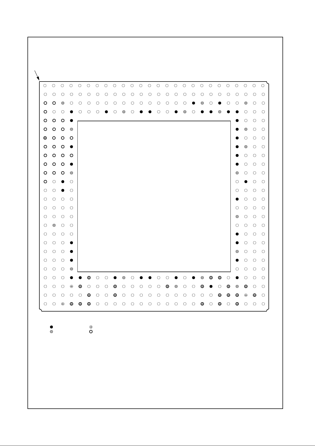
2.1 PIN ASSIGNMENTS
The tables in this section use several common abbreviations. Table 2-1 lists the mnemonics and their meanings.
Figure 2-2 shows the pin assignment for the CS5530 with
Tables 2-2 and 2-3 listing the pin assignments sorted by
terminal number and alphabetically by signal name,
respectively.
In Section 2.2 “Signal Descriptions” a description of each
signal within its associated functional group is provided.
In the signal definitions, references to F0-F4, F1BAR,
F2BAR, F3BAR, F4BAR, and PCIUSB are made. These
terms relate to designated register spaces. Refer to Table
4-1 "PCI Configuration Address Register (0CF8h)" on
page 138 for details regarding these register spaces and
their access mechanisms.
Table 2-1. Pin Type Definitions
Mnemonic Definition
5VT Buffer is 5V tolerant
I Input pin
I/O Bidirectional pin
IBUF Input buffer
OOutput
OD Open-drain output structure that
allows multiple devices to share the
pin in a wired-ORconfiguration
PU Pull-upresistor
PD Pull-down resistor
smt Schmitt Trigger
t/s Tri-state signal
VDD (PWR) Power pin
VSS (GND) Ground pin
# The "#" symbol at theend of a signal
name indicates that the active, or
asserted state occurs when the signal
is at a lowvoltage level. When "#"is
not present after the signal name, the
signal is asserted when at a high volt-
age level.
www.national.com 14 Revision 4.1
Signal Definitions (Continued)
Geode™ CS5530
Figure 2-2. TBGA Pin Assignment Diagram
Order Number: 25420-03
1234567891011121314151617181920
21 22 23 24 25 26
A
B
C
D
E
F
G
H
J
K
L
M
N
P
R
T
U
V
W
Y
AA
AB
AC
AD
AE
AF
Index Corner
PIX0 PIX1 PIX2 PIX7 PIX10 VCLK PIX12 PIX16 PIX19 DCLK VDAT0 VDAT5 PCLK INTA# AD0 AD7 AD9 AD12 AD10 AD15 PAR SERR# DVSL# C/BE2# AD17 AD16
ENADISP TVCLK PIX4 PIX5 VSYNC PIX8 VDVAL PIX15 PIX18 VDRDY PIX22 VDAT6 VDAT2 INTD# AD3 AD5 AD6 C/BE0# AD11 AD14 C/BE1# PERR# TRDY# IRDY# AD18 AD19
FPVSY FPHSY VDD PIX3 PIX11 HSYN PIX14 PIX17 PIX21 PIX23 VDAT3 VDAT7 VDAT1 PRST# INTC# AD2 AD4 VSS VDD AD13 VSS LOCK# FRAM# VDD AD21 AD22
FPD11 NC TEST VSS PIX6 PIX9 PIX13 VSS PIX20 VDD VDAT4 VSS VSS AD1 INTB# VSS VDD AD8 VSS VSS VDD VSS VSS GNT# AD26 C/BE3#
FPHSYO FPD10 FPVSYO VSS VSS AD20 AD23 STOP#
FPD9 DISENO FPD17 VDD VSS VDD AD24 AD27
FPD8 FPD5 FPD7 FPD6 VSS AD25 AD28 AD29
FPD4 FPD15 FPD16 VSS VSS VDD AD31 HDRQ#
FPD3 FPD1 FPD2 ENBKL VSS AD30 REQ# PCICLK
FPD14 FPD13 FPD0 VSS VSS POR# CPURST SUSP#
FPD12 ENVDD CKEVEN VDD VDD SUSP3V SUSPA# PSERL
FPCLK DDCSCL VSS DDCSDA PLDVD VSS PLVAA PLRO
HSYNO VSYNO VSS AVDD3 PLP PLAGS PLAGD PLDGN
AVSS4 AVSS5 IOUTR IOUTG VSS 14MHZ SMI# INTR
IOUTB AVSS1 IREF AVSS2 IRQ13 DIOW0# DIOR1# DIOR0#
VREF XVREFI AVDD2 AVSS3 VDD DDCK1# DIOW1# DDCK0#
AVDD1 VDD SYNC SDATI IDED7 IDED6 IDEA0 IDEA1
SDATO BITCLK PCBEEP PWREN VSS IDED8 IDED10 DCS0#
USBCLK NC OVRCUR# VSS VSS IDEA2 DRST# IDED5
D–PT1 D+PT1 NC VSS VDD IDED11 IDED9 DCS1#
D–PT2 D+PT2 NC VSS VSS IDED1 IDED12 IDED4
NC NC NC VDD IDED15 IDED2 IDED13 IDED3
NC NC NC VSS VSS SA3 DCK7# DCK1# VSS VDD IOW# VSS VSS IRQ3 MCS16# VSS IRQ14 VSS VDD SA10 GPIO5 GPIO0 VSS DREQ1 IDED14 IDED0
NC NC NC SMEMR# SA5 ISACLK DCK6# DCK0# SA2 SA19 SA16 DRQ1 DRQ3 IRQ7 SLTCH VDD IRQ15 DRQ5 SA9 VSS GPTCS# GPIO4 VDD SA14 IORDY0 DREQ0
NC NC 32K KRMCS# IRQ9 SA1 DCK5# AEN SA0 DRQ2 SA18 IOR# IRQ5 IRQ8# IRQ4 IRQ10 SBHE# DRQ0 MEMR# DRQ6 SA12 SA13 GPIO6 GPIO1 SA15 IORDY1
NC NC SMEMW# SA7 SA6 SA4 DCK3# DCK2# BALE 0WS# CHRDY SA17 IRQ1 IRQ6 TC CS16# IRQ12 IRQ11 SA8 MEMW# SA11 DRQ7 GPIO7 GPIO3 GPIO2 GPCS#
1234567891011121314151617181920
21 22 23 24 25 26
A
B
C
D
E
F
G
H
J
K
L
M
N
P
R
T
U
V
W
Y
AA
AB
AC
AD
AE
AF
Geode™ CS5530
I/O Companion
Top View
Note: Signal names have been abbreviated in this f ig ure due to space constraints.
= GND terminal
= PWR terminal
= Multiplexed signal
= Changes function in ISA Master Mode
Revision 4.1 15 www.national.com
Signal Definitions (Continued)
Geode™ CS5530
Table 2-2. 352 TBGA Pin Assignments - Sorted by Pin Number
Pin
No.
Signal Name
Limited
ISA Mode
ISA Master
Mode
A1 PIXEL0
A2 PIXEL1
A3 PIXEL2
A4 PIXEL7
A5 PIXEL10
A6 VID_CLK
A7 PIXEL12
A8 PIXEL16
A9 PIXEL19
A10 DCLK
A11 VID_DATA0
A12 VID_DATA5
A13 PCLK
A14 INTA#
A15 AD0
A16 AD7
A17 AD9
A18 AD12
A19 AD10
A20 AD15
A21 PAR
A22 SERR#
A23 DEVSEL#
A24 C/BE2#
A25 AD17
A26 AD16
B1 ENA_DISP
B2 TVCLK
B3 PIXEL4
B4 PIXEL5
B5 VSYNC
B6 PIXEL8
B7 VID_VAL
B8 PIXEL15
B9 PIXEL18
B10 VID_RDY
B11 PIXEL22
B12 VID_DATA6
B13 VID_DATA2
B14 INTD#
B15 AD3
B16 AD5
B17 AD6
B18 C/BE0#
B19 AD11
B20 AD14
B21 C/BE1#
B22 PERR#
B23 TRDY#
B24 IRDY#
B25 AD18
B26 AD19
C1 FP_VSYNC No Function
C2 FP_HSYNC No Function
C3 VDD
C4 PIXEL3
C5 PIXEL11
C6 HSYNC
C7 PIXEL14
C8 PIXEL17
C9 PIXEL21
C10 PIXEL23
C11 VID_DATA3
C12 VID_DATA7
C13 VID_DATA1
C14 PCI_RST#
C15 INTC#
C16 AD2
C17 AD4
C18 VSS
C19 VDD
C20 AD13
C21 VSS
C22 LOCK#
C23 FRAME#
C24 VDD
C25 AD21
C26 AD22
D1 FP_DATA11 SA11
D2 NC
D3 TEST
D4 VSS
D5 PIXEL6
D6 PIXEL9
D7 PIXEL13
D8 VSS
D9 PIXEL20
D10 VDD
D11 VID_DATA4
D12 VSS
D13 VSS
D14 AD1
D15 INTB#
D16 VSS
D17 VDD
D18 AD8
D19 VSS
D20 VSS
D21 VDD
D22 VSS
D23 VSS
D24 GNT#
Pin
No.
Signal Name
Limited
ISA Mode
ISA Master
Mode
D25 AD26
D26 C/BE3#
E1 FP_HSYNC_OUT SMEMW#
E2 FP_DATA10 SA10
E3 FP_VSYNC_OUT SMEMR#
E4 VSS
E23 VSS
E24 AD20
E25 AD23
E26 STOP#
F1 FP_DATA9 SA9
F2 FP_DISP_ENA_OUT No Function
F3 FP_DATA17 MASTER#
F4 VDD
F23 VSS
F24 VDD
F25 AD24
F26 AD27
G1 FP_DATA8 SA8
G2 FP_DATA5 SA5
G3 FP_DATA7 SA7
G4 FP_DATA6 SA6
G23 VSS
G24 AD25
G25 AD28
G26 AD29
H1 FP_DATA4 SA4
H2 FP_DATA15 SA15
H3 FP_DATA16 SA_OE#
H4 VSS
H23 VSS
H24 VDD
H25 AD31
H26 HOLD_REQ#
J1 FP_DATA3 SA3
J2 FP_DATA1 SA1
J3 FP_DATA2 SA2
J4 FP_ENA_BKL No Function
J23 VSS
J24 AD30
J25 REQ#
J26 PCICLK
K1 FP_DATA14 SA14
K2 FP_DATA13 SA13
K3 FP_DATA0 SA0
K4 VSS
K23 VSS
K24 POR#
K25 CPU_RST
K26 SUSP#
L1 FP_DATA12 SA12
Pin
No.
Signal Name
Limited
ISA Mode
ISA Master
Mode
www.national.com 16 Revision 4.1
Signal Definitions (Continued)
Geode™ CS5530
L2 FP_ENA_VDD No Function
L3 FP_CLK_EVEN No Function
L4 VDD
L23 VDD
L24 SUSP_3V
L25 SUSPA#
L26 PSERIAL
M1 FP_CLK NoFunction
M2 DDC_SCL
M3 VSS
M4 DDC_SDA
M23 PLLDVD
M24 VSS
M25 PLLVAA
M26 PLLRO
N1 HSYNC_OUT
N2 VSYNC_OUT
N3 VSS
N4 AVDD3(DAC)
N23 PLLLP
N24 PLLAGS
N25 PLLAGD
N26 PLLDGN
P1 AVSS4(ICAP)
P2 AVSS5(DAC)
P3 IOUTR
P4 IOUTG
P23 VSS
P24 CLK_14MHZ
P25 SMI#
P26 INTR
R1 IOUTB
R2 AVSS1(DAC)
R3 IREF
R4 AVSS2(ICAP)
R23 IRQ13
R24 IDE_IOW0#
R25 IDE_IOR1#
R26 IDE_IOR0#
T1 VREF
T2 EXTVREFIN
T3 AVDD2(VREF)
T4 AVSS3(VREF)
T23 VDD
T24 IDE_DACK1#
T25 IDE_IOW1#
T26 IDE_DACK0#
U1 AVDD1(DAC)
U2 VDD
U3 SYNC
U4 SDATA_IN
Pin
No.
Signal Name
Limited
ISA Mode
ISA Master
Mode
U23 IDE_DATA7
U24 IDE_DATA6
U25 IDE_ADDR0
U26 IDE_ADDR1
V1 SDATA_OUT
V2 BIT_CLK
V3 PC_BEEP
V4 POWER_EN
V23 VSS
V24 IDE_DATA8
V25 IDE_DATA10
V26 IDE_CS0#
W1 USBCLK
W2 NC
W3 OVER_CUR#
W4 VSS
W23 VSS
W24 IDE_ADDR2
W25 IDE_RST#
W26 IDE_DATA5
Y1 D–_PORT1
Y2 D+_PORT1
Y3 NC
Y4 VSS
Y23 VDD
Y24 IDE_DATA11
Y25 IDE_DATA9
Y26 IDE_CS1#
AA1 D–_PORT2
AA2 D+_PORT2
AA3 NC
AA4 VSS
AA23 VSS
AA24 IDE_DATA1
AA25 IDE_DATA12
AA26 IDE_DATA4
AB1 NC
AB2 NC
AB3 NC
AB4 VDD
AB23 IDE_DATA15
AB24 IDE_DATA2
AB25 IDE_DATA13
AB26 IDE_DATA3
AC1 NC
AC2 NC
AC3 NC
AC4 VSS
AC5 VSS
AC6 SA3/SD3 SD3
AC7 DACK7#
Pin
No.
Signal Name
Limited
ISA Mode
ISA Master
Mode
AC8 DACK1#
AC9 VSS
AC10 VDD
AC11 IOW#
AC12 VSS
AC13 VSS
AC14 IRQ3
AC15 MEMCS16#
AC16 VSS
AC17 IRQ14
AC18 VSS
AC19 VDD
AC20 SA10/SD10 SD10
AC21 GPIO5/SA21 SA21
AC22 GPIO0
AC23 VSS
AC24 IDE_DREQ1
AC25 IDE_DATA14
AC26 IDE_DATA0
AD1 NC
AD2 NC
AD3 NC
AD4 SMEMR#/RTCALE
AD5 SA5/SD5 SD5
AD6 ISACLK
AD7 DACK6#
AD8 DACK0#
AD9 SA2/SD2 SD2
AD10 SA19
AD11 SA16
AD12 DRQ1
AD13 DRQ3
AD14 IRQ7
AD15 SA_LATCH SA_DIR
AD16 VDD
AD17 IRQ15
AD18 DRQ5
AD19 SA9/SD9 SD9
AD20 VSS
AD21 GPORT_CS#
AD22 GPIO4/SA20 SA20
AD23 VDD
AD24 SA14/SD14 SD14
AD25 IDE_IORDY0
AD26 IDE_DREQ0
AE1 NC
AE2 NC
AE3 CLK_32K
AE4 KBROMCS#
AE5 IRQ9
AE6 SA1/SD1 SD1
Pin
No.
Signal Name
Limited
ISA Mode
ISA Master
Mode
Table 2-2. 352 TBGA Pin Assignments - Sorted by Pin Number (Continued)
Revision 4.1 17 www.national.com
Signal Definitions (Continued)
Geode™ CS5530
AE7 DACK5#
AE8 AEN
AE9 SA0/SD0 SD0
AE10 DRQ2
AE11 SA18
AE12 IOR#
AE13 IRQ5
AE14 IRQ8#
AE15 IRQ4
AE16 IRQ10
AE17 SBHE#
AE18 DRQ0
AE19 MEMR#
AE20 DRQ6
AE21 SA12/SD12 SD12
AE22 SA13/SD13 SD13
Pin
No.
Signal Name
Limited
ISA Mode
ISA Master
Mode
AE23 GPIO6/SA22 SD22
AE24 GPIO1/SDATA_IN2
AE25 SA15/SD15 SD15
AE26 IDE_IORDY1
AF1 NC
AF2 NC
AF3 SMEMW#/RTCCS#
AF4 SA7/SD7 SD7
AF5 SA6/SD6 SD6
AF6 SA4/SD4 SD4
AF7 DACK3#
AF8 DACK2#
AF9 BALE
AF10 ZEROWS#
AF11 IOCHRDY
AF12 SA17
Pin
No.
Signal Name
Limited
ISA Mode
ISA Master
Mode
AF13 IRQ1
AF14 IRQ6
AF15 TC
AF16 IOCS16#
AF17 IRQ12
AF18 IRQ11
AF19 SA8/SD8 SD8
AF20 MEMW#
AF21 SA11/SD11 SD11
AF22 DRQ7
AF23 GPIO7/SA23 SA23
AF24 GPIO3
AF25 GPIO2
AF26 GPCS#
Pin
No.
Signal Name
Limited
ISA Mode
ISA Master
Mode
Table 2-2. 352 TBGA Pin Assignments - Sorted by Pin Number (Continued)

www.national.com 18 Revision 4.1
Signal Definitions (Continued)
Geode™ CS5530
Table 2-3. 352 TBGA Pin Assignments - Sorted Alphabetically by S ignal Name
Signal Name
Pin Type
(Note 1)
Buffer
Type
(Note 2)
Pin
No.
Limited ISA
Mode
ISA Master
Mode
AD0
I/O, t/s, 5VT PCI A15
AD1 I/O, t/s, 5VT PCI D14
AD2 I/O, t/s, 5VT PCI C16
AD3 I/O, t/s, 5VT PCI B15
AD4 I/O, t/s, 5VT PCI C17
AD5 I/O, t/s, 5VT PCI B16
AD6 I/O, t/s, 5VT PCI B17
AD7 I/O, t/s, 5VT PCI A16
AD8 I/O, t/s, 5VT PCI D18
AD9 I/O, t/s, 5VT PCI A17
AD10 I/O, t/s, 5VT PCI A19
AD11 I/O, t/s, 5VT PCI B19
AD12 I/O, t/s, 5VT PCI A18
AD13 I/O, t/s, 5VT PCI C20
AD14 I/O, t/s, 5VT PCI B20
AD15 I/O, t/s, 5VT PCI A20
AD16 I/O, t/s, 5VT PCI A26
AD17 I/O, t/s, 5VT PCI A25
AD18 I/O, t/s, 5VT PCI B25
AD19 I/O, t/s, 5VT PCI B26
AD20 I/O, t/s, 5VT PCI E24
AD21 I/O, t/s, 5VT PCI C25
AD22 I/O, t/s, 5VT PCI C26
AD23 I/O, t/s, 5VT PCI E25
AD24 I/O, t/s, 5VT PCI F25
AD25 I/O, t/s, 5VT PCI G24
AD26 I/O, t/s, 5VT PCI D25
AD27 I/O, t/s, 5VT PCI F26
AD28 I/O, t/s, 5VT PCI G25
AD29 I/O, t/s, 5VT PCI G26
AD30 I/O, t/s, 5VT PCI J24
AD31 I/O, t/s, 5VT PCI H25
AEN O 8mA AE8
AVDD1(DAC) I, Analog -- U1
AVDD2(VREF) I, Analog -- T3
AVDD3(DAC) I, Analog -- N4
AVSS1 (DAC) I, Analog -- R2
AVSS2 (ICAP) I,Analog -- R4
AVSS3(VREF) I, Analog -- T4
AVSS4 (ICAP) I,Analog -- P1
AVSS5 (DAC) I, Analog -- P2
BALE O8mAAF9
BIT_CLK I, 5VT IBUF V2
C/BE0# I/O, t/s, 5VT PCI B18
C/BE1# I/O, t/s, 5VT PCI B21
C/BE2# I/O, t/s, 5VT PCI A24
C/BE3# I/O, t/s, 5VT PCI D26
CLK_14MHZ IsmtP24
CLK_32K I/O, 5VT 4 mA AE3
CPU_RST O8mAK25
DACK0# O8mAAD8
DACK1# O8mAAC8
DACK2# O8mAAF8
DACK3# O8mAAF7
DACK5# O 8 mA AE7
DACK6# O8mAAD7
DACK7# O8mAAC7
DCLK O8mAA10
DDC_SCL O 8 mA M2
DDC_SDA I/O, 5VT 8mA M4
DEVSEL# I/O, t/s, 5VT PCI A23
D–_PORT1 I/O USB Y1
D+_PORT1 I/O USB Y2
D–_PORT2 I/O USB AA1
D+_PORT2 I/O USB AA2
DRQ0 I, 5VT IBUF AE18
DRQ1 I, 5VT IBUF AD12
DRQ2 I, 5VT IBUF AE10
DRQ3 I, 5VT IBUF AD13
DRQ5 I, 5VT IBUF AD18
DRQ6 I, 5VT IBUF AE20
DRQ7 I, 5VT IBUF AF22
ENA_DISP IIBUFB1
EXTVREFIN I, Analog -- T2
FP_CLK No Function O 8 mA M1
FP_CLK_EVEN No Function O8mAL3
FP_DA TA0 SA0 I/O 8 mA K3
FP_DA TA1 SA1 I/O 8 mA J2
FP_DA TA2 SA2 I/O 8 mA J3
FP_DA TA3 SA3 I/O 8 mA J1
FP_DA TA4 SA4 I/O 8 mA H1
FP_DA TA5 SA5 I/O 8 mA G2
FP_DA TA6 SA6 I/O 8 mA G4
FP_DA TA7 SA7 I/O 8 mA G3
FP_DA TA8 SA8 I/O 8 mA G1
FP_DA TA9 SA9 I/O 8 mA F1
FP_DATA10 SA10 I/O 8 mA E2
FP_DATA11 SA11 I/O 8 mA D1
FP_DATA12 SA12 I/O 8 mA L1
FP_DATA13 SA13 I/O 8 mA K2
FP_DATA14 SA14 I/O 8 mA K1
FP_DATA15 SA15 I/O 8 mA H2
FP_DATA16 SA_OE# O8mAH3
FP_DATA17 MASTER# I/O 8 mA F3
FP_DISP_ENA_OUT No Function O8mAF2
FP_ENA_BKL No Function O8mAJ4
FP_ENA_VDD No Function O8mAL2
FP_HSYNC No Function IIBUFC2
FP_HSYNC_OUT SMEMW# O8mAE1
FP_VSYNC No Function IIBUFC1
FP_VSYNC_OUT SMEMR# O8mAE3
FRAME# I/O, t/s, 5VT PCI C23
Signal Name
Pin Type
(Note 1)
Buffer
Type
(Note 2)
Pin
No.
Limited ISA
Mode
ISA Master
Mode
Revision 4.1 19 www.national.com
Signal Definitions (Continued)
Geode™ CS5530
GNT# I, 5VT PCI D24
GPCS# O4mAAF26
GPIO0 I/O, 5VT 8 mA AC22
GPIO1/SDATA_IN2 I/O, 5VT 8 mA AE24
GPIO2 I/O, 5VT 8 mA AF25
GPIO3 I/O, 5VT 8 mA AF24
GPIO4/SA20 SA20 I/O, 5VT 8 mA AD22
GPIO5/SA21 SA21 I/O, 5VT 8 mA AC21
GPIO6/SA22 SA22 I/O, 5VT 8 mA AE23
GPIO7/SA23 SA23 I/O, 5VT 8 mA AF23
GPORT_CS# O8mAAD21
HOLD_REQ# (strap pin) I/O, 5VT PCI H26
HSYNC IIBUFC6
HSYNC_OUT O16mAN1
IDE_ADDR0 O8mAU25
IDE_ADDR1 O8mAU26
IDE_ADDR2 O8mAW24
IDE_CS0# O8mAV26
IDE_CS1# O8mAY26
IDE_DACK0# O8mAT26
IDE_DACK1# O8mAT24
IDE_DATA0 I/O, 5VT 8 mA AC26
IDE_DATA1 I/O, 5VT 8 mA AA24
IDE_DATA2 I/O, 5VT 8 mA AB24
IDE_DATA3 I/O, 5VT 8 mA AB26
IDE_DATA4 I/O, 5VT 8 mA AA26
IDE_DATA5 I/O, 5VT 8 mA W26
IDE_DATA6 I/O, 5VT 8 mA U24
IDE_DATA7 I/O, 5VT 8 mA U23
IDE_DATA8 I/O, 5VT 8 mA V24
IDE_DATA9 I/O, 5VT 8 mA Y25
IDE_DATA10 I/O, 5VT 8 mA V25
IDE_DATA11 I/O, 5VT 8 mA Y24
IDE_DATA12 I/O, 5VT 8 mA AA25
IDE_DATA13 I/O, 5VT 8 mA AB25
IDE_DATA14 I/O, 5VT 8 mA AC25
IDE_DATA15 I/O, 5VT 8 mA AB23
IDE_DREQ0 I, 5VT IBUF AD26
IDE_DREQ1 I, 5VT IBUF AC24
IDE_IOR0# O8mAR26
IDE_IOR1# O8mAR25
IDE_IORDY0 I, 5VT IBUF AD25
IDE_IORDY1 I, 5VT IBUF AE26
IDE_IOW0# O8mAR24
IDE_IOW1# O8mAT25
IDE_RST# O8mAW25
INTA# I, 5VT IBUF A14
INTB# I,5VT IBUF D15
INTC# I, 5VT IBUF C15
INTD# I, 5VT IBUF B14
INTR (strap pin) I/O 4 mA P26
Signal Name
Pin Type
(Note 1)
Buffer
Type
(Note 2)
Pin
No.
Limited ISA
Mode
ISA Master
Mode
IOCHRDY I/O, OD, 5VT 8 mA AF11
IOCS16# I, 5VT IBUF AF16
IOR# I/O (PU), 5VT 8 mA AE12
IOUTB O,Analog R1
IOUTR O , Analog P3
IOUTG O, Analog P4
IOW# I/O (PU), 5VT 8 mA AC11
IRDY# I/O, t/s, 5VT PCI B24
IREF I, Analog R3
IRQ1 I, 5VT IBUF AF13
IRQ3 I, 5VT IBUF AC14
IRQ4 I, 5VT IBUF AE15
IRQ5 I, 5VT IBUF AE13
IRQ6 I, 5VT IBUF AF14
IRQ7 I, 5VT IBUF AD14
IRQ8# I, 5VT IBUF AE14
IRQ9 I, 5VT IBUF AE5
IRQ10 I, 5VT IBUF AE16
IRQ11 I, 5VT IBUF AF18
IRQ12 I, 5VT IBUF AF17
IRQ13 I, 5VT IBUF R23
IRQ14 I, 5VT IBUF AC17
IRQ15 I, 5VT IBUF AD17
ISACLK O16mAAD6
KBROMCS# O 4 mA AE4
LOCK# I/O, t/s, 5VT PCI C22
MEMCS16# I/O, OD, 5VT 8 mA AC15
MEMR# I/O (PU), 5VT 8 mA AE19
MEMW# I/O (PU), 5VT 8 mA AF20
NC -- -- AA3
NC -- -- AB1
NC -- -- AB2
NC -- -- AB3
NC -- -- AC1
NC -- -- AC2
NC -- -- AC3
NC -- -- AD1
NC -- -- AD2
NC -- -- AD3
NC -- -- AE1
NC -- -- AE2
NC -- -- AF1
NC -- -- AF2
NC -- -- D2
NC -- -- W2
NC -- -- Y3
OVER_CUR# I, 5VT IBUF W3
PAR I/O, t/s, 5VT PCI A21
PC_BEEP O4mAV3
PCICLK IsmtJ26
PCI_RST# O16mAC14
Signal Name
Pin Type
(Note 1)
Buffer
Type
(Note 2)
Pin
No.
Limited ISA
Mode
ISA Master
Mode
Table 2-3. 352 TBGA Pin Assignments - Sorted Alphabetically by Signal Name (Continued)

www.national.com 20 Revision 4.1
Signal Definitions (Continued)
Geode™ CS5530
PCLK IsmtA13
PERR# I/O, t/s, 5VT PCI B22
PIXEL0 IIBUFA1
PIXEL1 IIBUFA2
PIXEL2 IIBUFA3
PIXEL3 IIBUFC4
PIXEL4 IIBUFB3
PIXEL5 IIBUFB4
PIXEL6 IIBUFD5
PIXEL7 IIBUFA4
PIXEL8 IIBUFB6
PIXEL9 IIBUFD6
PIXEL10 IIBUFA5
PIXEL11 IIBUFC5
PIXEL12 IIBUFA7
PIXEL13 IIBUFD7
PIXEL14 IIBUFC7
PIXEL15 IIBUFB8
PIXEL16 IIBUFA8
PIXEL17 IIBUFC8
PIXEL18 IIBUFB9
PIXEL19 IIBUFA9
PIXEL20 IIBUFD9
PIXEL21 IIBUFC9
PIXEL22 IIBUFB11
PIXEL23 IIBUFC10
PLLAGD I, Analog -- N25
PLLAGS I, Analog -- N24
PLLDGN I,Analog -- N26
PLLDVD I, Analog -- M23
PLLLP I, Analog -- N23
PLLRO I,Analog -- M26
PLLVAA I,Analog -- M25
POR# IIBUFK24
POWER_EN O4mAV4
PSERIAL IIBUFL26
REQ# O,5VT PCI J25
SA0/SD0 SD0 I/O (PU), 5VT 8 mA AE9
SA1/SD1 SD1 I/O (PU), 5VT 8 mA AE6
SA2/SD2 SD2 I/O (PU), 5VT 8 mA AD9
SA3/SD3 SD3 I/O (PU), 5VT 8 mA AC6
SA4/SD4 SD4 I/O (PU), 5VT 8 mA AF6
SA5/SD5 SD5 I/O (PU), 5VT 8 mA AD5
SA6/SD6 SD6 I/O (PU), 5VT 8 mA AF5
SA7/SD7 SD7 I/O (PU), 5VT 8 mA AF4
SA8/SD8 SD8 I/O (PU), 5VT 8 mA AF19
SA9/SD9 SD9 I/O (PU), 5VT 8 mA AD19
SA10/SD10 SD10 I/O (PU), 5VT 8 mA AC20
SA11/SD11 SD11 I/O (PU), 5VT 8 mA AF21
SA12/SD12 SD12 I/O (PU), 5VT 8 mA AE21
SA13/SD13 SD13 I/O (PU), 5VT 8 mA AE22
Signal Name
Pin Type
(Note 1)
Buffer
Type
(Note 2)
Pin
No.
Limited ISA
Mode
ISA Master
Mode
SA14/SD14 SD14 I/O (PU), 5VT 8 mA AD24
SA15/SD15 SD15 I/O (PU), 5VT 8 mA AE25
SA16 I/O (PU), 5VT 8 mA AD11
SA17 I/O (PU), 5VT 8 mA AF12
SA18 I/O (PU), 5 VT 8 mA AE11
SA19 I/O (PU), 5VT 8 mA AD10
SA_LATCH SA_DIR O4mAAD15
SBHE# I/O (PU), 5VT 8 mA AE17
SDAT A_IN I, 5VT IBUF U4
SDAT A_OUT O4mAV1
SERR# I/O, OD, 5VT PCI A22
SMEMR#/RTCALE O4mAAD4
SMEMW#/RTCCS# O4mAAF3
SMI# I/O 4 mA P25
STOP# I/O, t/s, 5VT PCI E26
SUSP# O4mAK26
SUSPA# IIBUFL25
SUSP_3V I/O 4 mA L24
SYNC O4mAU3
TC O8mAAF15
TEST IIBUFD3
TRDY# I/O, t/s, 5VT PCI B23
TVCLK I,5VT 4 mA B2
USBCLK IsmtW1
VDD PWR -- D10
VDD PWR -- D17
VDD PWR -- AB4
VDD PWR -- AC10
VDD PWR -- AC19
VDD PWR -- AD16
VDD PWR -- AD23
VDD PWR -- C19
VDD PWR -- C24
VDD PWR -- C3
VDD PWR -- D21
VDD PWR -- F24
VDD PWR -- F4
VDD PWR -- H24
VDD PWR -- L23
VDD PWR -- L4
VDD PWR -- T23
VDD PWR -- U2
VDD PWR -- Y23
VID_CLK IsmtA6
VID_DATA0 IIBUFA11
VID_DATA1 IIBUFC13
VID_DATA2 IIBUFB13
VID_DATA3 IIBUFC11
VID_DATA4 IIBUFD11
VID_DATA5 IIBUFA12
VID_DATA6 IIBUFB12
Signal Name
Pin Type
(Note 1)
Buffer
Type
(Note 2)
Pin
No.
Limited ISA
Mode
ISA Master
Mode
Table 2-3. 352 TBGA Pin Assignments - Sorted Alphabetically by Signal Name (Continued)
Revision 4.1 21 www.national.com
Signal Definitions (Continued)
Geode™ CS5530
Notes: 1) S ee Table 2-1 on page13 for pin type definitions.
2) See Table5-6 "DC Character istics (at Recommended
Operating Conditions)" on page 228 for more information. IBUF refers to input buffer.
VID_DATA7 IIBUFC12
VID_RDY O8mAB10
VID_VAL IIBUFB7
VREF I, Analog -- T1
VSS GND -- D12
VSS GND -- D13
VSS GND -- D16
VSS GND -- AA23
VSS GND -- AA4
VSS GND -- AC12
VSS GND -- AC13
VSS GND -- AC16
VSS GND -- AC18
VSS GND -- AC23
VSS GND -- AC4
VSS GND -- AC5
VSS GND -- AC9
VSS GND -- AD20
VSS GND -- C18
VSS GND -- C21
VSS GND -- D19
VSS GND -- D20
VSS GND -- D22
VSS GND -- D23
VSS GND -- D4
VSS GND -- D8
VSS GND -- E23
VSS GND -- E4
VSS GND -- F23
VSS GND -- G23
Signal Name
Pin Type
(Note 1)
Buffer
Type
(Note 2)
Pin
No.
Limited ISA
Mode
ISA Master
Mode
VSS GND -- H23
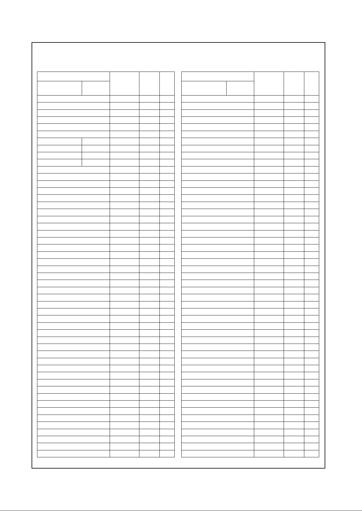
VSS GND -- H4
VSS GND -- J23
VSS GND -- K23
VSS GND -- K4
VSS GND -- M24
VSS GND -- M3
VSS GND -- N3
VSS GND -- P23
VSS GND -- V23
VSS GND -- W23
VSS GND -- W4
VSS GND -- Y4
VSYNC IIBUFB5
VSYNC_OUT O16mAN2
ZEROWS# I, 5VT IBUF AF10
Signal Name
Pin Type
(Note 1)
Buffer
Type
(Note 2)
Pin
No.
Limited ISA
Mode
ISA Master
Mode
Table 2-3. 352 TBGA Pin Assignments - Sorted Alphabetically by Signal Name (Continued)

www.national.com 22 Revision 4.1
Signal Definitions (Continued)
Geode™ CS5530
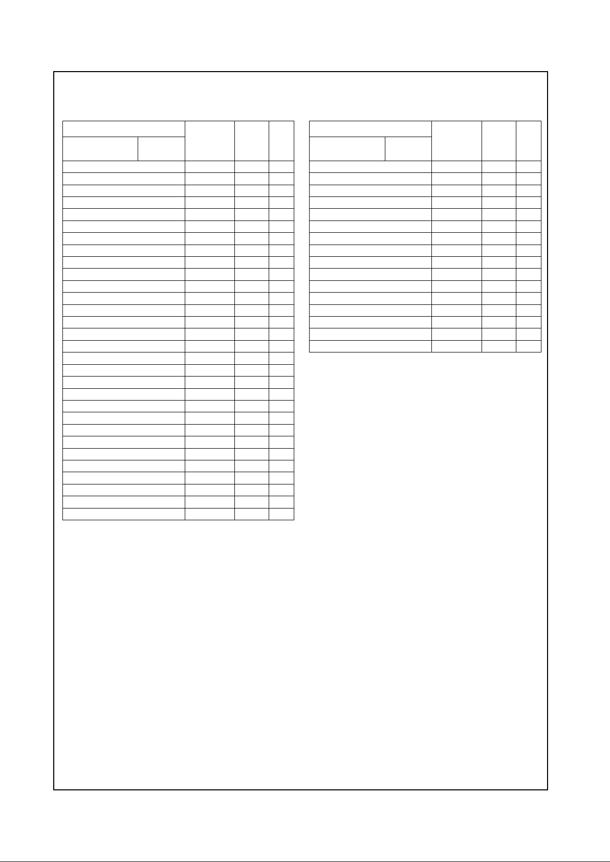
2.2 SIGNAL DESCRIPTIONS
2.2.1 Reset Interface
Signal Name
Pin
No. Type Description
PCI_RST# C14 O PCI Reset
PCI_RST# resets the PCI bus and is asserted while POR# is asserted,
and for approximately 9 ms following the deassertion of POR#.
POR# K24 I
smt
Power On Reset
POR# is the system reset signal generated from the power supply to indicate that the system should be reset.
CPU_RST K25 O CPU Reset
CPU_RST resets the CPU and is asserted while POR# is asserted, and
for approximately 9 ms following the deassertion of POR#.
2.2.2 Clock Interface
Signal Name
Pin
No. Type Description
PCICLK J26 I PCI Clock
The PCI clock is used to drivemost circuitry of the C S5530.
TVCLK B2 I
5VT
Television Clock
The TVCLK is an input from a digital NTSC/PAL converter which is optionally re-driven back out onto the DCLK signal under software program control. This is only used if interfacing to a compatible digital NTSC/PAL
encoder device.
DCLK A10 O DOT Clock
DOT clock is generated by the CS5530 and typically connects to the processor to create the video pixel clock. The minimum frequency of DCLK is
10 MHz and the maximumis 200 MHz.
ISACLK AD6 O ISA Bus Clock
ISACLK is derivedfrom PCICLK and is typically programmed for approximately 8 MHz. F0 Index 50h[2:0] is used to program the ISA clock divisor.
CLK_14MHZ P24 I 14.31818 MHz Clock
DOT clock (DCLK) is derivedfrom this clock.
USBCLK W1 I USBCLK
This input is used as the clocksource for the USB. In this mode,a 48 MHz
clock source input is required.
CLK_32K AE3 I/O
5VT
32KHz Clock
CLK_32K is a 32.768 KHz clock used to generatereset signals,as well as
to maintain power management functionality. It shouldbe active when
power is applied to the CS5530.
CLK_32K can be an inputor an output. As an output CLK_32Kis internally derived from CLK_14MHZ. F0 Index 44h[5:4] are usedto program
this pin.

Revision 4.1 23 www.national.com
Signal Definitions (Continued)
Geode™ CS5530
2.2.3 CPU Interface
Signal Name
Pin
No. Type Description
INTR P26
Strap
Option
Pin
O CPU Interrupt Request
INTR is the level output from the integrated 8259 PICs and is asserted if
an unmasked interrupt request (IRQ
n
) is sampled active.
I StrapOptionSelectPin
Pin P26 is a strap option select pin.It is used to select whether the
CS5530 operates in Limited ISA or ISA Master mode.
ISA Limited Mode—Strap pin P26 low through a 10-kohm resistor.
ISA Master Mode—Strap pin P26 high through a 10-kohm resistor.
SMI# P25 I/O System Management Interrupt
SMI# is a level-sensitive interrupt to the CPU thatcan be configured to
assert on a number of different system events. After an SMI# assertion,
System Management Mode (SMM) is entered, and program execution
begins at the base of SMM address space.
Once asserted, SMI# remains active until all SMI sourcesare cleared.
IRQ13 R23 I
5VT
IRQ13
IRQ13 is an input from the processor indicating that a floating point error
was detected and that INTR should be asser ted.
PSERIAL L26 I Power Management Serial Interface
PSERIAL is the unidirectional serial data link between the GXLV processor and the CS5530. An 8-bit serialdata packet carries status on power
management events within the CPU. Data is clocked synchronous to the
PCICLK input clock.
SUSP# K26 O CPU Suspend
SUSP# asserted requests that the processor enter Suspend mode and
assert SUSPA#after completion. The SUSP# pin is deasserted after
detecting any Speedup or Resume event. If the SUSP#/SUSPA#handshake is configured as a system 3 Volt Suspend, the deassertion of
SUSP# is delayedto allow the system clock chip and the processor to stabilize.
The SUSP#/SUSPA# handshake occurs as a resultof a write to the Suspend Notebook CommandRegister (F0 Index AFh), or an expirationof the
Suspend Modulation OFF Count Register (F0 Index 94h) when Suspend
Modulation is enabled. Suspend Modulation is enabled via F0 Index
96h[0].
SUSPA# L25 I CPU Suspend Acknowledge
SUSPA# is a levelinput from the processor. When asserted it indicates
the CPU is in Suspend mode as aresult of SUSP# assertion or execution
of a HALT instruction.

www.national.com 24 Revision 4.1
Signal Definitions (Continued)
Geode™ CS5530
SUSP_3V L24 I/O Suspend 3 Volt Active
SUSP_3V can be connected to the output enable (OE) of a clock synthesis or buffer chip to stop the clocks to the system. SUSP_3V is asserted
on any write to SuspendNotebook Command Register (F0 Index AFh)
with bit 0 set in the Clock Stop Control Register (F0 Index BCh).
SUSP_3V is only asserted after the SUSP#/SUSPA# handshake.
As an input, SUSP_3V is sampled during power-on-resetto determine the
inactivestate. This allows the system designer to match the active state of
SUSP_3V to the inactive state for a clock driver output enabled with a pullup/down 10-kohm resistor. If pulled down, SUSP_3V is active high. If
pulled up, SUSP_3V is active low.
2.2.3 CPU Interface (Continued)
Signal Name
Pin
No. Type Description
2.2.4 PCI Interface
Signal Name
Pin
No. Type Description
AD[31:0] Refer
toTable
2-3
I/O
t/s
5VT
PCI Address/Data
AD[31:0] is a physical address during the first clock of a PCI transaction; it
is the data during subsequent clocks.
When the CS5530 is a PCI master, AD[31:0] are outputs during the
addressand write data phases, and are inputs during the read data phase
of a transaction.
When the CS5530 is a PCI slave, AD[31:0] are inputs during the address
and write data phases, and are outputs during the read data phase of a
transaction.
C/BE[3:0]# D26,
A24,
B21,
B18
I/O
t/s
5VT
PCI Bus Command and Byte Enables
During the address phase of a PCI transaction, C/BE[3:0]# defines the
bus command. During the data phase of a transaction, C/BE[3:0]# are the
data byte enables.
C/BE[3:0]# are outputs when the CS5530 is a PCI master and are inputs
when it is a PCI slave.
INTA#,
INTB#,
INTC#,
INTD#
A14,
D15,
C15,
B14
I
5VT
PCI Interrupt Pins
The CS5530 provides inputs for the optional “level-sensitive” PCI interrupts (also known in industry terms as PIRQx#). These interrupts may be
mapped to IRQs of the internal 8259s usingPCI Interrupt Steering Registers 1 and 2 (F0 Index 5Ch and 5Dh).
The USB controller uses INTA#as its output signal. Refer to PCIUSB
Index 3Dh.
REQ# J25 O
5VT
PCI Bus Request
The CS5530 asserts REQ# in response to a DMA request or ISA master
request to gain ownership of the PCI bus. The REQ#and GNT# signals
areusedtoarbitrateforthePCIbus.
REQ# should connect to the REQ0# of the GXLVprocessor and function
as the highest-priority PCI master.

Revision 4.1 25 www.national.com
Signal Definitions (Continued)
Geode™ CS5530
GNT# D24 I
5VT
PCI Bus Grant
GNT# is asserted by an arbiter that indicates to the CS5530 thataccess
to the PCI bus has been granted.
GNT# should connect to GNT0# of the GXLV processor and function as
the highest-priority PCI master.
HOLD_REQ# H26
Strap
Option
Pin
O PCI Bus Hold Request
This pin’s function as HOLD_REQ# is no longer applicable.
I
5VT
StrapOptionSelectPin
Pin H26 is a strap option select pin. It allows selection of whichaddress
bitsareusedastheIDSEL.
Strap pin H26 low: IDSEL = AD28 (Chipset Register Space) and AD29
(USB Register Space)
Strap pin H26 high: IDSEL= AD26 (Chipset Register Space) and AD27
(USB Register Space)
FRAME# C23 I/O
t/s
5VT
PCI Cycle Frame
FRAME# is asserted to indicate the start and duration of a transaction. It
is deasserted on the final data phase.
FRAME# is an input when the CS5530is a PCI slave.
IRDY# B24 I/O
t/s
5VT
PCI Initiator Ready
IRDY# is driven by the master to indicate valid data on a write transaction,
or that it is ready to receive data on a read transaction.
When the CS5530 is a PCI slave, IRDY# is an input thatcan delay the
beginning of a write transaction or the completion of a read transaction.
Waitcycles are inserted until both IRDY#and TRDY# are asserted
together.
TRDY# B23 I/O
t/s
5VT
PCI Target Ready
TRDY# is asserted by a PCI slave to indicate it is ready to complete the
current data transfer.
TRDY# is an input that indicates a PCI slave has driven valid data on a
read or a PCI slave is ready to accept data fromthe CS5530 on a write.
TRDY# is an output that indicates theCS5530 has placed valid data on
AD[31:0] during a read or is ready to acceptthe data from a PCI master
on a write.
Waitcycles are inserted until both IRDY#and TRDY# are asserted
together.
STOP# E26 I/O
t/s
5VT
PCI Stop
As an input, STOP# indicates that a PCI slavewants to terminate the current transfer. The transfer will either be aborted or retried. STOP# is also
used to end a burst.
As an output, STOP# is asser ted with TRDY# to indicate a target disconnect, or without TRDY#to indicate a target retry. The CS5530 will assert
STOP#during any cache linecrossings if in singletransfer DMA mode or
if busy.
2.2.4 PCI Interface (Continued)
Signal Name
Pin
No. Type Description

www.national.com 26 Revision 4.1
Signal Definitions (Continued)
Geode™ CS5530
LOCK# C22 I/O
t/s
5VT
PCI Lock
LOCK# indicates an atomic operation that may require multiple transactions to complete.
If the CS5530 is currently the target of a LOCKed transaction, any other
PCI master request with the CS5530as the target is forced to retry the
transfer.
The CS5530 does not generate LOCKed transactions.
DEVSEL# A23 I/O
t/s
5VT
PCI Device Select
DEVSEL# is asserted by a PCI slave, to indicate to a PCI master and subtractivedecoder that it is the target of the current transaction.
As an input, DEVSEL# indicates a PCI slavehas responded to the current
address.
As an output, DEVSEL# is asserted one cycle after the assertion of
FRAME# and remains asserted to the end of atransaction as the result of
a positive decode. DEVSEL# is asserted four cycles after the assertion of
FRAME# if DEVSEL#has not been asserted by another PCI device when
the CS5530 is programmed to be the subtractive decode agent. The subtractivedecode sample point is configured in F0Index 41h[2:1]. Subtractive decode cycles are passedto the ISA bus.
PAR A21 I/O
t/s
5VT
PCI Parity
PAR is the parity signal driven to maintain even parity across AD[31:0]
and C/BE[3:0]#.
The CS5530 drives PARone clock after the address phase and one clock
after each completed data phase of write transactions as a PCI master. It
also drives PAR one clock after each completed data phaseof read transactions as a PCI slave.
PERR# B22 I/O
t/s
5VT
PCI Parity Error
PERR# is pulsed by a PCI device to indicate that a parity error was
detected.If a parity error was detected, PERR# is a sserted by a PCI slave
during a write data phase and by a PCI master during a read data phase.
When the CS5530 is a PCI master, PERR# is anoutput during read transfers and aninput during w rite transfers.When the CS5530 is aPCI slave,
PERR# is an input during read transfers and an output during write transfers.
Parity detection is enabled through F0 Index 04h[6]. An NMI is generated
if I/O Port 061h[2] is set. PERR# can assert SERR# if F0 Index 41h[5] is
set.
SERR# A22 I/O
OD
5VT
PCI System Error
SERR# is pulsed by a PCI device to indicatean address parity error, data
parity error on a specialcycle command, or other fatal system errors.
SERR# is an open-drain output reporting an error condition, and an input
indicating that the CS5530 should generate an NMI. As an input, SERR#
is asserted for a single clock by the slave reporting the error.
System error detection is enabled with F0 Index 04h[8]. An NMI is generated if I/O Port 061h[2]is set. PERR# can assert SERR# if F0 Index
41h[5] is set.
2.2.4 PCI Interface (Continued)
Signal Name
Pin
No. Type Description

Revision 4.1 27 www.national.com
Signal Definitions (Continued)
Geode™ CS5530
2.2.5 ISA B us Interface
Signal Name
Pin
No. Type Description
SA_LATCH/
SA_DIR
AD15 O Limited ISA Mode: System AddressLatch
This signal is used to latchthe destination address, which is multiplexed
on bits [15:0] of the SA/SD bus.
ISA Master Mode: System Address Direction
Controls the direction of the external 5.0V tolerant transceiver on bits
[15:0] of the SA bus. When low, the SA bus is drivenout. When high, the
SA bus is driven into the CS5530 by the external transceiver.
SA_OE#/
FP_DATA16
H3 O Limited ISA Mode: Flat Panel Data Port Line 16
Refer to Section 2.2.11 “Display Interface” on page 34 for this signal’s definition.
O ISA Master Mode: System Address Transceiver Output Enable
Enables the external transceiver on bits [15:0] of the SA bus.
MASTER#/
FP_DATA17
F3 O Limited ISA Mode: Flat Panel Data Port Line 17
Refer to Section 2.2.11 “Display Interface” on page 34 for this signal’s definition.
I ISA Master Mode: Master
The MASTER# input asserted indicates an ISA bus master is driving the
ISA bus.
SA23/GPIO7 AF23 I/O
5VT
Limited ISA Mode: System Address Bus Lines 23 through 20 or
General Purpose I/Os 7 through4
These pins can function either as the upper four bits of the SA busor as
general purpose I/Os. Programming is done through F0 Index43h, bits 6
and 2.
Refer to Section 2.2.9 “GamePort and General Purpose I/O Interface” on
page 32 for further detailswhen used as GPIOs.
SA22/GPIO6 AE23
SA21/GPIO5 AC21
SA20/GPIO4 AD22
ISA Master Mode: System AddressBus Lines 23 through 20
The pins function only as the four MSB (most significant bits) of the SA
bus.
SA[19:16] AD10,
AE11,
AF12,
AD11
I/O
PU
5VT
System Address Bus Lines 19 through 16
Refer to SA[15:0] signal description.
SA[15:0]/SD[15:0] Refer
to
Table
2-3
I/O
PU
5VT
Limited ISA Mode: System Address Bus / System Data Bus
This bus carries both the addresses and data for all ISA cycles. Initially,
the address is placed on the bus and then SA_LATCHis asserted for
externallatches to latch the address. At some time later,the data is put on
the bus, for a read,or the bus direction is changed to an input,for a write.
Pins designated as SA/SD[15:0] are internallyconnected to a 20-kohm
pull-up resistor.
ISA Master Mode: System Data Bus
These pins perform only as SD[15:0] and pins FP_DATA[15:0] take on the
functions of SA[15:0].
Pins designated as SA/SD[15:0] are internallyconnected to a 20-kohm
pull-up resistor.

www.national.com 28 Revision 4.1
Signal Definitions (Continued)
Geode™ CS5530
SMEMW#/
FP_HSYNC_OUT
E1 O Limited ISA Mode: Flat Panel Horizontal Sync Output
Refer to Section 2.2.11 “Display Interface” on page 34 for this signal’s definition.
Note that if Limited ISA Mode of operation is selected, SMEMW# is available on pin AF3 (multiplexed with RTCCS#).
ISA Master Mode: System Memory Write
SMEMW# is asserted for any memory write accesses below 1 MB. It
enables 8-bit memory slaves to decode the memory address on SA[19:0].
SMEMR#/
FP_VSYNC_OUT
E3 O Limited ISA Mode: Flat PanelVertical Sync Output
Refer to Section 2.2.11 “Display Interface” on page 34 for this signal’s definition.
Note that if Limited ISA Mode of operation is selected, SMEMR# is available on pin AD4 (multiplexedwith RTCALE).
ISA Master Mode: System M emory Read
SMEMR# is asserted for memory read accesses below 1 MB. It enables
8-bit memory slaves to decode the memory address on SA[19:0].
SMEMW#/
RTCCS#
AF3 O System Memory Write / Real-Time Clock Chip Select
If Limited ISA Mode of operation has been selected, then SMEMW# can
be output on this pin. SMEMW# is asserted for any memory write
accesses below 1 MB. It enables 8-bit memory slaves to decode the
memory address on SA[19:0].
RTCCS# is a chip select to an external real-time clock chip. This signal is
activated on reads or writes to I/O Port 071h
Function selection is made through F0 Index 53h[2]: 0 = SMEMW#,
1=RTCCS#.
SMEMR#/
RTCALE
AD4 O System Memory Read / Real-Time Clock Address Latch Enable
If Limited ISA Mode of operation has been selected, then SMEMR# can
be output on this pin. SMEMR# is asserted for memory read accesses
below 1 MB. It enables 8-bit memory slaves to decode the memory
address on SA[19:0].
RTCALE is a signal telling an externalreal-time clock chip to latch the
address, which is on the SD bus.
Function selection is made through F0 Index 53h[2]: 0 = SMEMR#,
1=RTCALE.
SBHE# AE17 I/O
PU
5VT
System Bus High Enable
The CS5530 or ISA masterasserts SBHE# to indicatethat SD[15:8] will
be used to transfer a byte at an odd address.
SBHE# is an outputduring non-ISA masterDMA operations. It is driven
as the inversion of AD0 during 8-bit DMA cycles. It is forced low for all 16bit DMA cycles.
SBHE# is an input during ISA master operations.
This pin is internally connected to a 20-kohm pull-up resistor.
BALE AF9 O Buffered Address Latch Enable
BALE indicates when SA[23:0] and SBHE# are valid and may be latched.
For DMA transfers, BALE remains asserted until the transfer is complete.
2.2.5 ISA Bus Interface (Continued)
Signal Name
Pin
No. Type Description

Revision 4.1 29 www.national.com
Signal Definitions (Continued)
Geode™ CS5530
IOCHRDY AF11 I/O
OD
5VT
I/O Channel Ready
IOCHRDY deasserted indicates that an ISA slaverequires additional wait
states.
When the CS5530 is an ISA slave, IOCHRDY is an output indicating additional wait states are required.
ZEROWS# AF10 I
5VT
Zero Wait States
ZEROWS#asserted indicates that an ISA 8- or 16-bit memory slave can
shorten the current cycle. The CS5530samples this signal in the phase
after BALE is asserted. If asserted, it shortens 8-bit cycles to three
ISACLKs and 16-bitcycles to twoISACLKs.
IOCS16# AF16 I
5VT
I/O Chip Select 16
IOCS16#is asserted by 16-bit ISA I/O devices basedon an asynchronous
decode of SA[15:0] to indicate that SD[15:0] will be used to transfer data.
Note: 8-bit ISA I/O devices only use SD[7:0].
IOR# AE12 I/O
PU
5VT
I/O Read
IOR# is asserted to request an ISA I/O slave to drive data onto the data
bus.
This pin is internally connected to a 20-kohm pull-up resistor.
IOW# AC11 I/O
PU
5VT
I/O Write
IOW#is asserted to request an ISA I/O slave to accept data from the data
bus.
This pin is internally connected to a 20-kohm pull-up resistor.
MEMCS16# AC15 I/O
OD
5VT
Memory Chip Select 16
MEMCS16# is asserted by 16-bit ISA memory devices based on an asynchronous decode of SA[23:17] to indicate that SD[15:0] will be used to
transfer data.
Note: 8-bit ISA memory devices only use SD[7:0].
MEMR# AE19 I/O
PU
5VT
Memory Read
MEMR# is asserted for any memor y read accesses. It enables 16-bit
memory slaves to decode the memor y address on SA[23:0].
This pin is internally connected to a 20-kohm pull-up resistor.
MEMW# AF20 I/O
PU
5VT
Memory Write
MEMW# is asserted for any memory write accesses. It enables 16-bit
memory slaves to decode the memor y address on SA[23:0].
This pin is internally connected to a 20-kohm pull-up resistor.
AEN AE8 O Address Enable
AEN asserted indicates that a DMA transfer is in progress, informing I/O
devices to ignore the I/O cycle.
IRQ[15:14],[12:9],
[7:3], 1
Refer
to
Table
2-3
I
5VT
ISA Bus Interrupt Request
IRQ inputs indicate ISA devices or other devices requesting a CPU interrupt service.
IRQ8# AE14 I
5VT
Real-Time Clock Interrupt
IRQ8# is the (active-low) interrupt that can come from the external RTC
chip and indicates a date/time update has completed.
2.2.5 ISA Bus Interface (Continued)
Signal Name
Pin
No. Type Description

www.national.com 30 Revision 4.1
Signal Definitions (Continued)
Geode™ CS5530
DRQ[7:5],
DRQ[3:0]
Refer
to
Table
2-3
I
5VT
DMA Request - Channels [7:5], [3:0]
DRQ inputs are asserted by ISA DMA devices to request a DMAtransfer.
The request must remain asserted until the corresponding DACK is
asserted.
DACK[7:5]#,
DACK[3:0]#
Refer
to
Table
2-3
O DMA Acknowledge - Channels [7:5], [3:0]
DACK outputs are asserted to indicate when a DRQ is granted and the
start of a DMA cycle.
TC AF15 O Terminal Count
TC signals the final data transfer of a DMA transfer.
2.2.5 ISA Bus Interface (Continued)
Signal Name
Pin
No. Type Description
2.2.6 ROM Interface
Signal Name
Pin
No. Type Description
KBROMCS# AE4 O Keyboard/ROM Chip Select
KBROMCS# is the enable pin for the BIOS ROM and for the keyboard
controller. For ROM accesses, KBROMCS# is asserted for ISA memory
accesses programmed at F0 Index 52h[2:0].
For keyboard controller accesses, KBROMCS# is asserted for I/O
accesses to I/O Ports 060h, 062h, 064h,and 066h.

Revision 4.1 31 www.national.com
Signal Definitions (Continued)
Geode™ CS5530
2.2.7 IDE Interface
Signal Name
Pin
No. Type Description
IDE_RST# W25 O IDE Reset
This signal resets all the devices that are attached to the IDE interface.
IDE_ADDR[2:0] W24,
U26,
U25
O IDE Address Bits
These address bits are used toaccess a register or data port in a device
on the IDE bus.
IDE_DATA[15:0] Refer
to
Table
2-3
I/O
5VT
IDE Data Lines
IDE_DATA[15:0] transfers data to/from the IDE devices.
IDE_IOR0# R26 O IDE I/O Read for Channels 0 and 1
IDE_IOR0# is the read signal for Channel 0, and IDE_IOR1#is the read
signal for Channel 1. Each signal is asserted on read accesses to the corresponding IDE port addresses.
When in Ultra DMA/33 mode, these signals are redefined:
Read Cycle — DMARDY0# and DMARDY1#
Write Cycle — STROBE0and STROBE1
IDE_IOR1# R25 O
IDE_IOW0# R24 O IDE I/O Write forChannels 0 and 1
IDE_IOW0# is the write signal for Channel 0, and IDE_IOW1# is the read
signal for Channel 1. Each signalis asserted on write accessesto corresponding the IDE port addresses.
When in Ultra DMA/33 mode, these signals are redefined:
Read Cycle — STOP0 and STOP1
WriteCycle—STOP0andSTOP1
IDE_IOW1# T25 O
IDE_CS0# V26 O IDE Chip Selects
The chip select signals are used to select the command block registers in
an IDE device.
IDE_CS1# Y26 O
IDE_IORDY0 AD25 I
5VT
I/O Ready Channels 0 and 1
When deasserted, these signals extend the transfer cycleof any host register access when the device is not ready to respond to the data transfer
request.
When in Ultra DMA/33 mode, these signals are redefined:
Read Cycle — STROBE0and STROBE1
WriteCycle—DMARDY0#andDMARDY1#
IDE_IORDY1 AE26 I
5VT
IDE_DREQ0 AD26 I
5VT
DMA Request Channels 0 and 1
The DREQ is used to request a DMA transfer from the CS5530. The
direction of the transfers are determined by the IDE_IOR/IOW signals.
IDE_DREQ1 AC24 I
5VT
IDE_DACK0# T26 O DMA Acknowledge Channels 0 and 1
The DACK# acknowledges the DREQ request to initiateDMA transfers.
IDE_DACK1# T24 O

www.national.com 32 Revision 4.1
Signal Definitions (Continued)
Geode™ CS5530
2.2.8 USB Interface
Signal Name
Pin
No. Type Description
POWER_EN V4 O Power Enable
This pin enables the power to a self-powered USB hub.
OVER_CUR# W3 I
5VT
Over Current
This pin indicates the USB hub has detected a n overcurrent on the USB.
D+_PORT1 Y2 I/O USB Port 1 Data Positive
This pin is the Universal Serial Bus Data Positive for port 1.
D–_PORT1 Y1 I/O USB Port 1 Data Minus
This pin is the Universal Serial Bus Data Minus for port 1.
D+_PORT2 AA2 I/O USB Port 2 Data Positive
This pin is the Universal Serial Bus Data Positive for port 2.
D–_PORT2 AA1 I/O USB Port 2 Data Minus
This pin is the Universal Serial Bus Data Minus for port 2.
2.2.9 Game Port and General Purpose I/O Interface
Signal Name
Pin
No. Type Description
GPORT_CS# AD21 O Game Port Chip Select
GPORT_CS# is asserted upon any I/O reads or I/O writes to I/O Port
200h and 201h.
GPCS# AF26 O General Purpose Chip Select
GPCS# is asserted upon any I/O access that matches the I/O address in
the General Purpose Chip Select Base Address Register (F0 Index 70h)
and the conditions set in the General Purpose Chip Select Control Register (F0 Index 72h).
GPIO7/SA23 AF23 I/O
5VT
Limited ISA Mode: General Purpose I/Os 7 through 4 or
System Address Bus Lines 23 through 20
These pins can function either as general purpose I/Os or as the upper
four bits of the SA bus. Selection is done throughF0 Index 43h[6,2].
Refer to GPIO[3:2] signal description for GPIO function description.
GPIO6/SA22 AE23
GPIO5/SA21 AC21
GPIO4/SA20 AD22
ISA Master Mode: System AddressBus Lines 23 through 20
These pins function as the four MSB (most significant bits) of the SA bus.
GPIO3 AF24 I/O
5VT
General Purpose I/Os 3 and 2
GPIOs can be programmed to operate as inputsor outputs via F0 Index
90h. As an input,the GPIO can be configured to generate an external
SMI. Additional configuration can selectif the SMI# is generated on the
rising or falling edge. GPIO external SMI generation/edge selection is
done in F0 Index 92h and 97h.
GPIO2 AF25 I/O
5VT

Revision 4.1 33 www.national.com
Signal Definitions (Continued)
Geode™ CS5530
GPIO1/
SDATA_IN2
AE24 I/O
5VT
General Purpose I/O 1 or Serial Data Input 2
This pin can function either as a general purpose I/O or as a second serial
data input pin if twocodecs are used in the system.
In order for this pin to function as SDATA_IN2, it must first be configured
as an input (F0 Index 90h[1] = 0). Then setting F3BAR+Memory Offset
08h[21] = 1 selects the pin to function asSDATA_IN2.
Refer to GPIO[3:2] signal description for GPIO function description.
GPIO0 AC22 I/O
5VT
General Purpose I/O 0
Refer to GPIO[3:2] signal description for GPIO function description.
2.2.9 Game Port and General Purpose I/O Interface (Continued)
Signal Name
Pin
No. Type Description
2.2.10 Audio Interface
Signal Name
Pin
No. Type Description
BIT_CLK V2 I
5VT
Audio Bit Clock
The serial bit clock from the codec.
SDATA_OUT V1 O Serial Data I/O
This output transmits audio serial data to the codec.
SDATA_IN U4 I
5VT
Serial Data Input
This input receives serial data from the codec.
SYNC U3 O Serial Bus Synchronization
This bit is asserted to synchronize the transfer of data between the
CS5530 and the AC97 codec
PC_BEEP V3 O PC Beep
Legacy PC/AT speaker output.

www.national.com 34 Revision 4.1
Signal Definitions (Continued)
Geode™ CS5530
2.2.11 Display Interface
Signal Name
Pin
No. Type Description
Pixel Port
PCLK A13 I Pixel Clock
This clock is used to sample data on the PIXEL input port. It runs at the
graphics DOT clock (DCLK) rate.
PIXEL[23:0] Refer
to
Table
2-3
I Pixel Data Port
This is the input pixel data from the processor’s display controller. If
F4BAR+Memory Offset 00h[29] is reset, the data is sent inRGB 8:8:8 format. Otherwise, the pixeldata is sent in RGB 5:6:5 format which has been
dithered by the processor. The other eight bits are used in conjunction
with VID_DATA[7:0] to provide 16-bit video data. Thisbus is sampled by
the PCLK input.
ENA_DISP B1 I Display Enable Input
This signal qualifies active data on the pixel input port. It is used to qualify
active pixel data for all display modes and configurations and is not specific to flat panel display.
Display CRT
HSYNC C6 I Horizontal Sync Input
This is the CRT horizontal sync input from the processor’sdisplay controller.It is used to indicate the start of a new video line. This signalis pipelined for the appropriate number of clock stages to remain in sync with the
pixel data. A separate output (HSYNC_OUT) is provided to re-drive the
CRT and flat panel interfaces.
HSYNC_OUT N1 O Horizontal Sync Output
This is the horizontal sync output to the CRT. It represents a delayed version of the input horizontal sync signal with the appropriate pipeline delay
relative to the pixel data. The pipeline delay and polarity of this signal are
programmable.
VSYNC B5 I Vertical Sync Input
This is the CRT vertical sync input from the processor’s display controller.
It is used to indicate the start of a newframe. This signal is pipelined for
the appropriate number of clock stages to remainin sync with the pixel
data. A separate output (VSYNC_OUT)is provided to re-drive the CRT
and flat panel interfaces.
VSYNC_OUT N2 O Vertical Sync Output
This is the vertical sync output to the CRT. It represents a delayed version
of the input vertical sync signal with the appropriate pipeline delay relative
to the pixel data. The pipeline delay and polarity of thissignal are programmable.
DDC_SCL M2 O DDC Serial Clock
This is the serial clockfor the VESA Display Data Channel interface. It is
used for monitor communications. The DDC2B standard is supported by
this interface.

Revision 4.1 35 www.national.com
Signal Definitions (Continued)
Geode™ CS5530
DDC_SDA M4 I/O
5VT
DDC Serial Data
This is the bidirectional serial data signal for the VESA Display Data
Channel interface. It is used to monitor communications. The DDC2B
standard is supported by this interface.
The direction of this pin can be configured through F4BAR+Memory Offset 04h[24]: 0 = Input;1 = Output.
IREF
(Video DAC)
R3 I
Analog
VDAC Current Reference Input
Connect a 732 ohm resistor between this pin and AVSS (analog ground
for Video DAC).
VREF
(Video DAC)
T1 I
Analog
VDAC Voltage Reference Output
Unused DAC output. Connect a 0.1 µF capacitor between this pin and
AVSS (analog ground for Video DAC).
EXTVREFIN
(Video DAC)
T2 I
Analog
External Voltage Reference Pin
When using an external voltage reference, connect this pin to a 1.235V
voltage reference.
AVDD1 (DAC) U1 I
Analog
Analog Power for Video DAC
These pins provide power to the analog portions of the Video DAC.
AVDD2 (VREF) T3
AVDD3 (DAC) N4
AVSS1 (DAC) R2 I
Analog
Analog Ground for Video DAC
These pins provide the ground plane connections to the analog portions
of the Video DAC.
AVSS2 (ICAP) R4
AVSS3 (VREF) T4
AVSS4 (ICAP) P1
AVSS5 (DAC) P2
IOUTR
(Video DAC)
P3 O
Analog
Red DAC Output
Red analog output.
IOUTG
(Video DAC)
P4 O
Analog
Green DAC Output
Green analog output.
IOUTB
(Video DAC)
R1 O
Analog
Blue DAC Output
Blue analog output.
Display TFT/TV
FP_DATA17/
MASTER#
F3 O Limited ISA Mode: Flat Panel Data Port Line 17
Refer to FP_DATA[15:0] signal description.
I ISA Master Mode: Master
Refer to Section2.2.5 “ISA Bus Interface” on page 27 forthis signal’s definition.
FP_DATA16/
SA_OE#
H3 O Limited ISA Mode: Flat Panel Data Port Line 16
Refer to FP_DATA[15:0] signal description.
O ISA Master Mode: System Address Transceiver Output Enable
Refer to Section2.2.5 “ISA Bus Interface” on page 27 forthis signal’s definition.
2.2.11 Display Interface (Continued)
Signal Name
Pin
No. Type Description

www.national.com 36 Revision 4.1
Signal Definitions (Continued)
Geode™ CS5530
FP_DATA[15:0]/
SA[15:0]
Refer
to
Table
2-3
O Limited ISA Mode: F lat PanelData Port Lines 15 through 0
This is the data port to an attached active matrix TFT panel. This port may
optionally be tied to a DSTN formatter chip, LVDS transmitter, or digital
NTSC/PAL encoder.
F4BAR+Memory Offset 04h[7] enables the flat paneldata bus:
0 = FP_DATA[17:0] is forced low
1 = FP_DATA[17:0]is driven based uponpower sequence control
I/O ISA Master Mode: System AddressBus Lines 15 through 0
These pins function as SA[15:0] and the pins designated as SA/SD[15:0]
function only as SD[15:0].
Note that SA[19:16] are dedicated address pins and GPIO[7:4] function
as SA[23:20] only.
FP_CLK M1 O Limited ISA Mode: Flat Panel Clock
This is the clock for the flat panel interface.
-- ISA Master Mode: No Function
In the ISA Master mode of operation, the CS5530 cannot support TFT flat
panels or TV controllers.
FP_CLK_EVEN L3 O Limited ISA Mode: Flat Panel Even Clock
This is an optional output clock for a set of external latches used to demultiplexthe flat panel data bus into two channels (odd/even). Typically
thiswouldbeusedtointerfacetoapairofLVDStransmittersdrivingan
XGA resolution flat panel.
F4BAR+Memory Offset 04h[12] enables the FP_CLK_EVENoutput:
0 = Standard flatpanel
1 = XGA flat panel
-- ISA Master Mode: No Function
In the ISA Master mode of operation, the CS5530 can not support TFT flat
panels or TV controllers.
FP_HSYNC C2 I Limited ISA Mode: Flat Panel Horizontal Sync Input
This is the horizontal sync input reference from the processor’s display
controller. The timing of this signal is independent of the standard (CRT)
horizontal sync inputto allow a different timing relationship between the
flat panel and an attached CRT.
-- ISA Master Mode: No Function
In the ISA Master mode of operation, the CS5530 can not support TFT flat
panels or TV controllers.
FP_HSYNC_OUT
/SMEMW#
E1 O Limited ISA Mode: Flat Panel Horizontal Sync Output
This is the horizontal sync for an attachedactive matrix TFT flat panel.
This represents a delayed version of the input flat panel horizontal sync
signal with the appropriate pipeline delay relative to the pixel data.
ISA Master Mode: System Memory Write
Refer to Section2.2.5 “ISA Bus Interface” on page 28 forthis signal’s definition.
2.2.11 Display Interface (Continued)
Signal Name
Pin
No. Type Description

Revision 4.1 37 www.national.com
Signal Definitions (Continued)
Geode™ CS5530
FP_VSYNC C1 I Limited ISA Mode: Flat Panel Vertical Sync Input
This is the vertical sync input reference from the processor’s display controller. The timing of this signal is independent of the standard (CRT) vertical sync input to allow a differenttiming relationship betweenthe flat panel
andanattachedCRT.
-- ISA Master Mode: No Function
In the ISA Master mode of operation, the CS5530 can not support TFT flat
panels or TV controllers.
FP_VSYNC_OUT
/SMEMR#
E3 O Limited ISA Mode: Flat PanelVertical Sync Output
This is the vertical sync for an attached active matrix TFT flat panel. This
represents a delayed version of the input flat panelvertical sync signal
with the appropriate pipeline delay relative to the pixel data.
ISA Master Mode: System M emory Read
Refer to Section2.2.5 “ISA Bus Interface” on page 28 forthis signal’s definition.
FP_DISP_
ENA_OUT
F2 O Flat Panel Display Enable Output
This is the display enable for an attached active matrix TFT flat panel. This
signal qualifies active pixel data on the flat panelinterface.
-- ISA Master Mode: No Function
In the ISA Master mode of operation, the CS5530 can not support TFT flat
panels or TV controllers.
FP_ENA_VDD L2 O Flat Panel VDD Enable
This is the enable signal for the VDD supply to an attached flat panel. It is
under the control of power sequence control logic. Atransition on bit 6 of
the Display Configuration Register (F4BAR+Memory Offset04h) initiates
a power-up/down sequence.
-- ISA Master Mode: No Function
In the ISA Master mode of operation, the CS5530 can not support TFT flat
panels or TV controllers.
FP_ENA_BKL J4 O Flat Panel Backlight Enable Output
This is the enable signal for the backlight power supply to anattached flat
panel. It is under control of the power sequence control logic.
-- ISA Master Mode: No Function
In the ISA Master mode of operation, the CS5530 can not support TFT flat
panels or TV controllers.
Display MPEG
VID_DATA[7:0] C12,
B12,
A12,
D11,
C11,
B13,
C13,
A11
I Video Data Port
This is the input data for a video (MPEG)or graphics overlayin its native
form. For video overlay, this data is in an interleaved YUV 4:2:2 format.
For graphics overlay, the data is in RGB 5:6:5 format. This port operates
at the VID_CLK rate.
2.2.11 Display Interface (Continued)
Signal Name
Pin
No. Type Description

www.national.com 38 Revision 4.1
Signal Definitions (Continued)
Geode™ CS5530
VID_CLK A6 I Video Clock
This is the clock for the video port. Thisclock is completely asynchronous
to the input pixel clock rate.
VID_VAL B7 I Video Valid
This signal indicates that valid video data is beingpresented on the
VID_DATA input port. If the VID_RDYsignal is also asserted, the datawill
advance.
VID_RDY B10 O Video Ready
This signal indicates that the CS5530 is ready to receive the next piece of
video data on the VID_DATA port. If the VID_VAL signal is also asserted,
the data will advance.
2.2.11 Display Interface (Continued)
Signal Name
Pin
No. Type Description
2.2.12 DCLK PLL
Signal Name
Pin
No. Type Description
PLLLP N23 I
Analog
Loop Filter Capacitor Connection
The loop filter requires an external capacitor (optionally a series resistor
may be added) for adjustment of the loop filter response. The PLLLP pin
connects this capacitorto the on-chiploop filter.
PLLRO M26 I
Analog
VCO Center Frequency Set Resistor Connection
The center frequency of the VCO is set with an external resistor connected between thePLLRO and PLLAGS pins. This resistor sets a constant current that controls the center frequency of the VCO.
PLLAGS N24 I
Analog
Analog Sense Pin for Connection of External Components
This pin is used as the return connection for all externalcomponents. This
includesthe ground connection for the loop filter capacitor and the PLLRO
resistor.
PLLVAA M25 I
Analog
Analog PLL Power (VDD)
PLLVAA is the analog positive rail power connection to the PLL.
PLLAGD N25 I
Analog
Analog PLL Ground (VSS)
PLLAGD is the analog ground rail connection to the PLL.
PLLDVD M23 I
Analog
Digital PLL Power (VDD)
This pin is the digitalVDD power connection for the PLL.
PLLDGN N26 I
Analog
Digital PLL Ground
This pin is the digital ground (VSS) connectionfor the PLL.

Revision 4.1 39 www.national.com
Signal Definitions (Continued)
Geode™ CS5530
2.2.13 Power, Ground, and Reserved
Signal Name
Pin
No. Type Description
VDD Refer to
Table 2-3
(Total of
19)
PWR 3.3V (nominal) Power Connection
VSS Refer to
Table 2-3
(Total of
39)
GND Ground Connection
NC Refer to
Table 2-3
(Total of
17)
-- No Connection
This line should be left disconnected. Connecting it to a pull-up/-down
resistor or to an active signal could cause unexpectedresults and possible malfunctions.
2.2.14 Internal Test and Measurement
Signal Name
Pin
No. Type Description
TEST D3 I Test Mode
TEST should be tied low for normal operation.

www.national.com 40 Revision 4.1
Geode™ CS5530
3.0 Functional Description
The Geode CS5530 I/O companion provides many support functions for the GXLV processor. This chapter discusses the detailed operations of the CS5530 in two
categories: system-level activities and operations/programming of the major functional blocks.
The system-level discussion topics revolve around events
that affect the device as a whole unit and as an interface
with other chips (e.g., processor): Topics include:
• Processor Interface
- DisplaySubsystem Connections
- PSERIAL Pin Interface
•PCIBusInterface
- PCI Initiator
-PCITarget
- Special Bus Cycles - Shutdown/Halt
-PCIBusParity
- PCI Interrupt Routing Support
- Delayed Transactions
• Resets and Clocks
-Resets
-ISAClock
-DOTClock
• Power Management
- APM Support
- CPU Power Management
- Peripheral Power Management
All of the major functional blocks interact with the processor through the PCI bus, or via its own direct interface.
The major functional blocks are divided out as:
• PC/AT Compatibility Logic
- ISA Bus Interface
- ROM Interface
- Megacells
- I/O Port 092h and 061hSystem Control
- Keyboard Interface Function
- External Real-Time Clock Interface
• IDE Controller
- IDE Interface Signal
- IDE Configuration Registers
• XpressAUDIO
- Data Transport Hardware
- VSA Technology Support Hardware
• Display Subsystem Extensions
- Video Interface Configuration Registers
- Video Accelerator
- Video Overlay
-GammaRAM
- DisplayInterface
•USBInterface
- USB PCI Controller
- USB Host Controller
- USB Power Management
Note that this Functional Description section of the data
book describes many of the registers used for configuration of the CS5530; however, not all registers are reported
in detail. Some tables in the following subsections show
only the bits (not the entire register) associated with a
specific function being discussed. For access, register,
and bit information regarding all CS5530 registers refer to
Section 4.0 “Register Descriptions” on page 137.

Revision 4.1 41 www.national.com
Functional Description (Continued)
Geode™ CS5530
3.1 PROCESSOR INTERFACE
The CS5530 interface to the GXL V processor consists of
seven miscellaneous connections, the PCI bus interface
signals, plus the display controller connections. Figure 3-1
shows the interface requirements. Note that the PC/AT
legacy pins NMI, WM_RST, and A20M are all virtual functions executed in SMM (System Management Mode) by
the BIOS.
• PSERIALis a one-way serial bus from the processor to
the CS5530 used to communicate power-management
states and VSYNC information for VGA emulation.
• IRQ13 is aninput from the processor indicating that a
floating point error was detected and that INTR should
be asserted.
• INTR is the level output from the integrated 8259 PICs
and is asserted if an unmasked interrupt request
(IRQn) is sampled active.
• SMI# is a level-sensitive interrupt to the processor that
can be configured to assert on a number of different
system events.After an SMI# assertion, SMM is
entered and program executionbegins at the base of
the SMM address space. Once asserted, SMI#
remains active until the SMI source is cleared.
• SUSP# and SUSPA# are handshake pins for implementing CPU Clock Stop and clock throttling.
• CPU_RST resets the CPU and is asserted for approximately 9 ms after the negation of POR#.
• PCI bus interface signals.
• Display subsystem interface connections.
Figure 3-1. Processor Signal Connections
SERIALP
IRQ13
SMI#
INTR
SUSP#
SUSPA#
AD[31:0]
C/BE[3:0]#
PAR
FRAME#
IRDY#
TRDY#
STOP#
LOCK#
DEVSEL#
PERR#
SERR#
REQ0#
PSERIAL
IRQ13
SMI#
CPU_RST
INTR
SUSP#
SUSPA#
AD[31:0]
C/BE[3:0]#
PAR
FRAME#
IRDY#
TRDY#
STOP#
LOCK#
DEVSEL#
PERR#
SERR#
REQ#
GNT# GNT0#
Geode™ GXLVGeode™ CS5530
RESET
PCLK
CRT_HSYNC
CRT_VSYNC
PIXEL[17:0]
FP_HSYNC
FP_VSYNC
ENA_DISP
VID_VAL
VID_CLK
VID_DATA[7:0]
VID_RDY
PCLK
HSYNC
VSYNC
PIXEL[23:0]
FP_HSYNC
FP_VSYNC
ENA_DISP
VID_VAL
VID_CLK
VID_DATA[7:0]
VID_RDY
DCLKDCLK
I/O Companion Processor
Note: Refer to Figure 3-3 for correct interconnection
of PIXEL lines with the processor.
Note

www.national.com 42 Revision 4.1
Functional Description (Continued)
Geode™ CS5530
3.1.1 Display Subsystem Connections
When the GXL V processor is used in a system with the
CS5530, the need for an external RAMDAC is eliminated.
The CS5530 contains the DACs, a video accelerator
engine, and the TFT interface.
The CS5530 also supports both portable and desktop
configurations. Figure 3-2 shows the signal connections
for both types of systems.
Figure 3-3 details how PIXEL[17:0] on the processor connects with PIXEL[23:0] of the CS5530.
Figure 3-2. Portable/Desktop Display Subsystem Configurations
DCLK
PCLK
FP_HSYNC
FP_VSYNC
ENA_DISP
VID_RDY
VID_CLK
VID_DATA[7:0]
PIXEL[17:12]
PIXEL[11:6]
HSYNC
VSYNC
R[5:0]
G[5:0]
B[5:0]
CLK
VDD
12VBKL
Pin 13
Pin 14
Pin 3
Pin 2
Pin 1
Pwr
Cntrl
ENAB
VGA
Pin 15
Pin 12
Geode™ CS5530
I/O Companion
DCLK
PCLK
FP_HSYNC
FP_VSYNC
ENA_DISP
VID_RDY
VID_CLK
VID_DATA[7:0]
PIXEL[23:18]*
PIXEL[15:10]*
PIXEL[5:0]
VID_VAL
CRT_HSYNC
CRT_VSYNC
PIXEL[7:2]*
VID_VAL
HSYNC
VSYNC
FP_ENA_VDD
FP_ENA_BKL
FP_DISP_ENA_OUT
FP_HSYNC_OUT
FP_VSYNC_OUT
FP_CLK
FP_DATA[17:12]
FP_DATA[11:6]
FP_DAT A[5:0]
Logic
HSYNC_OUT
VSYNC_OUT
IOUTR
IOUTG
IOUTB
DDC_SCL
DDC_SDA
Note: *Connect PIX EL[17:16] PIXEL[9:8], and PIXEL[1:0] on the CS5530 to ground. See Figure 3-3.
Port
Portable
Configuration
TFT
Flat
R[5:0]
G[5:0]
B[5:0]
HSYNC
VSYNC
CLK
TV
NTSC/PAL
Encoder
Panel
Geode™
Processor
GXLV

Revision 4.1 43 www.national.com
Functional Description (Continued)
Geode™ CS5530
Figure 3-3. PIXEL Signal Connections
PIXEL17
PIXEL16
PIXEL15
PIXEL14
PIXEL13
PIXEL12
PIXEL11
PIXEL10
PIXEL9
PIXEL8
PIXEL7
PIXEL6
PIXEL5
PIXEL4
PIXEL3
PIXEL2
PIXEL1
Geode™ GXLV
Processor
Geode™ CS5530
I/O Companion
PIXEL0
PIXEL23
PIXEL22
PIXEL21
PIXEL20
PIXEL19
PIXEL18
PIXEL17
PIXEL16
PIXEL15
PIXEL14
PIXEL13
PIXEL12
PIXEL11
PIXEL10
PIXEL9
PIXEL8
PIXEL7
PIXEL6
PIXEL5
PIXEL4
PIXEL3
PIXEL2
PIXEL1
PIXEL0

www.national.com 44 Revision 4.1
Functional Description (Continued)
Geode™ CS5530
3.1.2 PSERIAL Pin Interface
The majority of the system power management logic is
implemented in the CS5530, but a minimal amount of
logic is contained within the GXL V processor to provide
information that is not externally visible (e.g., graphics
controller).
The processor implements a simple serial communications mechanism to transmit the CPU status to the
CS5530. The processor accumulates CPU events in an 8bit register (defined in Table 3-1) which it transmits serially
every 1 to 10 µs.
The packet transmitter holds the serial output pin (PSERIAL) low until the transmission interval counter has
elapsed. Once the counter has elapsed, the PSERIAL pin
is held high for two clocks to indicate the start of packet
transmission. The contents of the Serial Packet Register
are then shifted out starting from bit 7 down to bit 0. The
PSERIAL pin is heldhigh for one clock to indicate the end
of packet transmission and then remains low until the next
transmission interval. After the packet transmission is
complete, the processor’s Serial Packet Register’s contents are cleared.
The processor’sinput clock is used as the clock reference
for the serial packet transmitter.
Once a bit in the register is set, it remains set until the
completion of the next packet transmission. Successive
events of the same type that occur between packet transmissions are ignored. Multiple unique events between
packet transmissions accumulate in this register. The processor transmits the contents of the serial packet only
when a bit in the Serial Packet Register is set and the
interval counter has elapsed.
For more information on the Serial Packet Register referenced in Table 3-1, refer to the GXL V processor data
book.
The CS5530 decodes the serial packet after each transmission and performs the power management tasks
relatedtovideoretrace.
3.1.2.1 Video Retrace Interrupt
Bit 7 of the “Serial Packet” can be used to generate an
SMI whenever a video retrace occurs within the processor. This function is normally not used for power management but for SoftVGA routines.
Setting F0 Index 83h[2] = 1 (bit details on page 159)
enables this function. A read only status register located
at F1BAR+Memory Offset 00h[5] (bit details on page 180)
can be read to see if the SMI was caused by a video
retrace event.
Table 3-1. GXLV Processor Serial Packet
Register
Bit Description
7 Video IRQ: This bit indicates the occurrence of a video
vertical sync pulse. This bit is set at the same time that
the VINT (Vertical Interrupt) bit gets set in the
DC_TIMING_CFG register. The VINT bit has a corresponding enable bit (VIEN) in the DC_TIM_CFG register.
6 CPU Activity: This bit indicates the occurrence of a
level 1 cache miss thatwas not a result of an instruction fetch. This bit has a corresponding enable bit in
the PM_CNTL_TEN register.
5:2 Reserved
1 Programmable Address Decode: This bit indicates
the occurrence of a programmable memory address
decode. The bit is set based on the values of the
PM_BASE register and the PM_MASK register. The
PM_BASE register can be initialized to any address in
the full CPU address range.
0 Video D ecode: This bit indicates that the CPU has
accessed either the display controller registers or the
graphics m emory region. This bit has a corresponding
enable bit in the PM_CNTRL_TEN.

Revision 4.1 45 www.national.com
Functional Description (Continued)
Geode™ CS5530
3.2 PCI BUS INTERFACE
The PCI bus interface is compliant with the PCI Bus Specification Rev. 2.1.
The CS5530 acts as a PCI target for PCI cycles initiated
by the processor or other PCI master devices, or as an initiator for DMA, ISA, IDE, and audio master transfer cycles.
It supports positive decode for memory and I/O regions
and is the subtractive decode agent on the PCI bus. The
CS5530 also generates address and data parity and performs parity checking. A PCI bus arbiter is not part of the
CS5530; however, one is included in the GXLV processor.
The PCI Command Register, located at F0 Index 04h
(Table 3-2), provides the basic control over the CS5530’s
ability to respond and perform PCI bus accesses.
3.2.1 PCI Initiator
The CS5530 acts as a PCI bus master on b ehalf of the
DMA controller or ISA, IDE, and audio interfaces. The
REQ# and GNT# signals are used to arbitrate for the PCI
bus.
Note: In a GXLV processor-based system, the
REQ#/GNT# signals of the CS5530 should connect to the REQ0#/GNT0# of the processor. This
configurationensures that the CS5530 is treated
as a non-preemptable PCI master by the processor.
TheCS5530assertsREQ#inresponsetoabusmastering or DMA request for ownership of the PCI bus. GNT# is
asserted by the PCI arbiter (i.e., processor) to indicate
that access to the PCI bus has been granted to the
CS5530. The CS5530 then issues a grant to the DMA
controller. This mechanism prevents any deadlock situations across the bridge. Once granted the PCI bus, the
ISA master or DMA transfer commences.
If an ISA master executes an I/O access, that cycle
remains on the ISA bus and is not forwarded to the PCI
bus. The CS5530 performs only single transfers on the
PCI bus for legacy DMA cycles.
Table 3-2. PCI Command Register
Bit Description
F0 Index 04h-05h PCI Com mand Register (R/W) Reset Value = 0000h
15:10 Reserved: Set to 0.
9 Fast Back-to-Back Enable (Read Only): This function is not supported when the CS5530 is a master. It is always dis-
abled (always reads 0).
8 SERR#: Allow SERR# assertion on detection of special errors: 0 = Disable (Default);1=Enable.
7 Wait Cycle Control (Read Only): This function is not supported in the CS5530. It is always disabled
(always reads 0).
6 Parity Error: Allow the CS5530 to check for parity errors on PCI cycles for which it is a target, and to assert PERR# when
a parity error is detected: 0 = Disable (Default); 1 = Enable.
5 VGA Palette Snoop Enable (Read Only):This function is not supported in the CS5530. It is always disabled (always
reads 0).
4 Memory Write and Invalidate: Allow the CS5530 to do memory write and invalidate cycles, if the PCI Cache Line Regis-
ter (F0 Index 0Ch) is setto 16 bytes (04h). 0 = Disable (Default); 1 = Enable.
3 Special Cycles: Allow the CS 5530 t o respond to special cycles: 0 = Disable; 1 = Enable (Default).
This bit must be enabled to allow the CPU Warm Reset internal signal to be triggered from a CPU Shutdown cycle.
2 Bus Master: Allow the CS5530 bus mastering capa bilities: 0 = Disable; 1 = Enable (Default).
This bit must be set to 1.
1 Memory Space: Allow the CS5530 to respond to memory cycles from the PCI bus:
0 = Disable; 1 = Enable (Default).
0 I/O Space: Allow the CS5530 to respond to I/O cycles f rom the PCI bus: 0 = Disable; 1 = Enable (Default).

www.national.com 46 Revision 4.1
Functional Description (Continued)
Geode™ CS5530
3.2.2 PCI Target
The CS5530 positively decodes PCI transactions
intended for any internal registers, the ROM address
range, and several peripheral and user-defined address
ranges. For positive-decoded transactions, the CS5530 is
a medium responder. Table 3-3 lists the valid C/BE#
encoding for PCI target transactions.
The CS5530 acts as the subtractive agent in the system
since it contains the ISA bridge functionality. Subtractive
decoding ensures that all accesses not positively claimed
by PCI devices are forwarded to the ISA bus. The subtractive-decoding sample point can be configured as slow,
default,or disabled via F0 Index 41h[2:1]. Table 3-4 shows
these programming bits. Figure 3-4 shows the timing for
subtractive decoding.
Figure 3-4. Subtractive Decoding Timing
T able 3-3. PCI Command Encoding
C/BE[3:0]# Command Type
0000 Interrupt Acknowledge
0001 Special Cycles: Shutdown, AD[15:0] = 0000
Special Cycles: Halt, AD[15:0] = 0001
0010 I/O Read
0011 I/O Write
010x Reserved
0110 Me mory Read
0111 Me mory Write
100x Reserved
1010 Configuration Read
1011 Configuration Writ e
1100 Memory Read Multiple
(memory read only)
1101 Reserved
1110 M emory Read Line (memory read only)
1111 Me mory Write, Invalidate (memory write)
Table 3-4. Subtractive Decoding Related Bits
Bit Description
F0 Index 41h PCI Function Control Register 2 (R/W) Reset Val ue = 10h
2:1 Subtractive Decode: These bits determine the point at which the CS5530 accepts cycles that are not claimed by another
device. The CS5530 defaults to taking subtractive decode cycles in the default cycle clock, but can be moved up to the
Slow Decode cycle point if all other PCI devices decode in the fast or medium clocks. Disabling subtractive decode must
be done with care, as all ISA and ROM cycles are decoded subtractively.
00 = Default sample (4th clock from FRAME# active)
01 = Slow sample (3rd clock from FRAME# active)
1x = No subtractive decode
PCI_CLK
FRAME#
IRDY#
TRDY#
DEVSEL#
FAST MED SLOW SUB

Revision 4.1 47 www.national.com
Functional Description (Continued)
Geode™ CS5530
3.2.3 Special Bus Cycles–Shutdown/Halt
The PCI interface does not pass Special Bus Cycles to
the ISA interface, since special cycles by definition have
no destination. However, the PCI interface monitors the
PCI bus for Shutdown and Halt Special Bus Cycles.
Upon detection of a Shutdown Special Bus Cycle, a
WM_RST SMI is generated after a delay o f three PCI
clock cycles. PCI Shutdown Special Cycles are detected
when C/BE[3:0]# = 0001 during the address phase and
AD[31:0] = xxxx0000h during the data phase. C/BE[3:0]#
are also properly asserted during the dataphase.
Upon detection of a Halt Special Bus Cycle, the CS5530
completes the cycle by asserting TRDY#. PCI Halt Special Bus Cycles are detectedwhen CBE[3:0]# = 0001 during the address phase and AD[31:0] = xxxx0001h during
the data phase of a Halt cycle. CBE[3:0]# are also properly asserted during the data phase.
3.2.4 PCI Bus Parity
When the CS5530 is the PCI initiator, it generates
address parity for read and write cycles. It checks data
parity for read cycles and it generates data parity for wr ite
cycles. The PAR signal is an even-parity bit that is calculated across 36 bits of AD[31:0] plus C/BE[3:0]#.
By default,the CS5530 does not report parity errors. However, the CS5530 detects parity errors during the data
phase if F0 Index 04h[6] is set to 1. If enabled and a data
parity error is detected, the CS5530 asserts PERR#. It
also asserts SERR# if F0 Index 41h[5] is set to 1. This
allows NMI generation.
The CS5530 also detects parity errors during the address
phase if F0 Index 04h[6] is set. When parity errors are
detected during the address phase, SERR# is asserted
internally. Parity errors are reported to the CPU by
enabling the SERR# source in I/O Port 061h (Port B) control register. The CS5530 sets the corresponding error bits
in the PCI Status Register (F0 Index 06h[15:14]). Table 35 shows these programming bits.
If the CS5530 is the PCI master for a cycle and detects
PERR# asserted, itgenerates SERR# internally.
Table 3-5. PERR#/SE RR# Associated Register Bits
Bit Description
F0 Index 04h-05h PCI Com mand Register (R/W) Reset Value = 0000h
6 Parity Error: Allow the CS5530 to check for parity errors on PCI cycles for which it is a target, and to assert PERR# when
a parity error is detected: 0 = Disable (Default); 1 = Enable.
F0 Index 06h-07h PCI Status Register (R/W) Reset Value = 0280h
15 Detected Parity Error: This bit is set whenever a parity error is detected.
Write 1 to clear.
14 Signaled System Error: This bit is set whenever the CS5530 asserts SERR# active.
Write 1 to clear.
F0 Index 41h PCI Function Control Register 2 (R/W) Reset Val ue = 10h
5 PERR# Signals SERR#: Assert SERR# any time that PERR# is asserted or detected act ive by the CS5530 (allows
PERR# assertion to be cascaded to NMI (SMI) generation in the system): 0 = Dis able; 1 = Enable.

www.national.com 48 Revision 4.1
Functional Description (Continued)
Geode™ CS5530
3.2.5 PCI Interrupt Routing Support
The CS5530 allows the PCI interrupt signals INTA#,
INTB#, INTC#, and INTD# (also know in industry terms as
PIRQx#) to be mapped internally to any IRQ signal via
registerprogramming (shown in Table 3-6). Further details
are supplied in Section 3.5.4.4 “PCI Compatible Interrupts” on page 98 regarding edge/level sensitivity selection.
3.2.6 Delayed Transactions
The CS5530 suppor ts delayed transactions to prevent
slow PCI cycles from occupying too much bandwidth and
allows access for other PCItraffic.
Note: For systems which haveonly theGXLVprocessor
and CS5530 on the PCI bus, system performance
is improved if delayed transactions are disabled.
F0 Index 42h[5] and F0 Index 43h[1] are used to program
this function. Table 3-7 showsthese bit formats.
Table 3-6. PCI Interrupt Steering Registers
Bit Description
F0 Index 5Ch PCI Interrupt Steering Register 1 (R/W) Reset Value = 00h
7:4 INTB# Target Interrupt: Selects target interrupt for INTB#:
0000 = Disable 0100 = IRQ4 1000 = RSVD 1100 = IRQ 12
0001 = IRQ1 0101 = IRQ5 1001 = IRQ9 1101 = RSVD
0010 = RSVD 0110 = IRQ6 1010 = IRQ10 1110 = IRQ14
0011 = IRQ3 0111 = IRQ7 1011 = IRQ11 1111 = IRQ15
3:0 INTA# Target Interrupt: Selects target interrupt for INTA#:
0000 = Disable 0100 = IRQ4 1000 = RSVD ‘ 1100 = IRQ12
0001 = IRQ1 0101 = IRQ5 1001 = IRQ9 1101 = RSVD
0010 = RSVD 0110 = IRQ6 1010 = IRQ10 1110 = IRQ14
0011 = IRQ3 0111 = IRQ7 1011 = IRQ11 1111 = IRQ15
Note: The target interrupt must first be configured as level sensitive via I/O Port 4D0h and 4D1h in order to maintain PCI
interrupt compatibility
F0 Index 5Dh PCI Interrupt Steering Register 2 (R/W) Reset Value = 00h
7:4 INTD# Target Interrupt: Selects target interrupt for INTD#:
0000 = Disable 0100 = IRQ4 1000 = RSVD 1100 = IRQ 12
0001 = IRQ1 0101 = IRQ5 1001 = IRQ9 1101 = RSVD
0010 = RSVD 0110 = IRQ6 1010 = IRQ10 1110 = IRQ14
0011 = IRQ3 0111 = IRQ7 1011 = IRQ11 1111 = IRQ15
3:0 INTC# Target Interrupt: Selects target interrupt for INTC#:
0000 = Disable 0100 = IRQ4 1000 = RSVD 1100 = IRQ 12
0001 = IRQ1 0101 = IRQ5 1001 = IRQ9 1101 = RSVD
0010 = RSVD 0110 = IRQ6 1010 = IRQ10 1110 = IRQ14
0011 = IRQ3 0111 = IRQ7 1011 = IRQ11 1111 = IRQ15
Note: The target interrupt must first be configured as level sensitive via I/O Port 4D0h and 4D1h in order to maintain PCI
interrupt compatibility
Table 3-7. Delay Transaction Programming Bits
Bit Description
F0 Index 42h PCI Function Control Register 3 (R/ W ) Reset Value = ACh
5 Delayed Transactions: Allow delayed transactions on the PCI bus: 0 = Disable; 1 = Ena ble.
Also see F0 Index 43h[1].
F0 Index 43h USB Shadow Register (R/W) Reset Value = 03h
1 PCI Retry Cycles: When the CS5530 is a PCI target and the PCI buffer is not empty,allow PCI bus to retry cycles:
0 = Disable; 1 = Enable.
This bit works in conjunction with PCI bus delayed transactions bit. F0 Index 42h[ 5] must = 1 for this bit to be valid.

Revision 4.1 49 www.national.com
Funcitonal Description (Continued)
Geode™ CS5530
3.3 RESE TS AND CLOCKS
The operations of resets and clocks in the CS5530 are
described in this section of the Functional Description.
3.3.1 Resets
The CS5530 generates two reset signals, PCI_RST# to
the PCI bus and CPU_RST tothe GXLV processor. These
resets are generated after approximately 100 µs delay
from POR# active as depicted in Figure 3-5.
At any state, Power-on/Resume/Reset, the 14.31818 MHz
oscillator must be active for the resets to function.
3.3.2 ISA Clock
The CS5530 creates the ISACLK from dividing the PCICLK. For ISA compatibility, the ISACLK nominally runs at
8.33 MHz or less. The ISACLK dividers are programmed
via F0 Index 50h[2:0] as shown in Table 3-8.
Figure 3-5. CS5530 Reset
Table 3-8. ISACLK Divider Bits
Bit Description
F0 Index 50h PIT Control/ISA CLK Divider (R/W) Reset Value = 7Bh
2:0 ISA Clock Divisor: Determines the divisor of the PCI clock used to make the ISA clock, which is typically
programmed for approximately 8 MHz:
000 = Divide by one 100 = Divide by five
001 = Divide by two 101 = Divide by six
010 = Divide by three 110 = Divide by seven
011 = Divide by four 111 = Divide by eight
If PCI clock = 25 MHz, use setting of 010 (divide by 3). If PCI clock = 30 or 33 MHz, use a setting of 011 (divide by 4).
POR#
CPU_RST
PCI_RST#
100 µs
POR# minimum pulse width for CS5530 only (i.e., not a system specification) = 100 µs and 14 M Hz must be running.
9ms

www.national.com 50 Revision 4.1
Functional Description (Continued)
Geode™ CS5530
3.3.3 DOT Clock
The DOT clock (DCLK) is generated from the 14.31818
MHz input (CLK_14MHZ). A combination of a phase
locked loop (PLL), linear feedback shift register (LFSR)
and divisors are used to generate the desired frequencies
for the DOT clock. The divisors and LFSR are configurable through the F4BAR+Memory Offset 24h. The minimum frequency of DCLK is 10 MHz and the maximum is
200 MHz.
DCLK provides a video clock for the GXLV processor. For
applications that do not use the GXLV processor’s video,
this is an availableclock for general purpose use.
The system c lock distribution for a CS5530/GXLV processor based system is shown in Figure3-6.
Figure 3-6. System Clock Distribution
DCLKtoGXLVProcessor
M
U
X
DCLK
PLL
÷N
TVCLK from TV Controller
Clock
Geode™ CS5530
48 MHz Clock to USB of CS5530
PCICLK to GXLV Processor
PCICLK
PCICLK to PCI Related Device
PCICLK to PCI Bus
Geode™
SDRAMCLK to SDRAM
SDRAMCLK to SDRAM
SDRAMCLK to SDRAM
SDRAMCLK to SDRAM
14 MHz Clock to Super I/O
14.318 MHz
Crystal
32 KHz for Reset and
Power Management
14 MHz Clock to TV Controller
ISACLK to ISA Bus
SUSP_3V
OE#
from CS5530
24.576 MHz Clock to AC97 Codec
GXLV
Generator
14 MHz Clock
I/O Companion
Processor

Revision 4.1 51 www.national.com
Funcitonal Description (Continued)
Geode™ CS5530
3.3.3.1 DCLK Programming
The PLL contains an input divider (ID), feedback divider
(FD) and a post divider (PD). The programming of the
dividers is through F4BAR+Memory Offset 24h (see Table
3-9). The maximum output frequency is 300 MHz. The
output frequency is given by equation #1:
Equation #1:
DCLK = [CLK_14MHZ * FD] ÷ [PD *ID]
Condition:
140 MHz < [DCLK * PD] < 300 MHz
Where:
CLK_14MHZ is pin P24
FD is derived from N see equation #2 and #3:
PD is derived from bits [28:24]
ID is derived from bits[2:0]
Equation #2:
If FD is an odd number then: FD = 2*N +1
Equation #3:
If FD is an even number then: FD = 2*N +0
Where:
N is derived from bits[22:12]
+1 is achieved by settingbit 23 to 1.
+0 is achieved by clearingbit 23 to 0.
Example
Define Target Frequency:
Target frequency =135 MHz
Satisfy the “Condition”:
(140 MHz < [DCLK * PD] < 300 MHz)
140 MHz < [135 MHz * 2] < 300 MHz
Therefore PD = 2
Solve Equation #1:
DCLK = [CLK_14MHZ * FD] ÷ [PD *ID]
135 = [14.31818 * FD] ÷ [2 * ID]
135 = [7.159 * FD] ÷ ID
18.86 = FD ÷ ID
Guess: ID = 7, Solve f or FD
FD = 132.02
Solve Equation #2 or #3:
FD = 2*N +1 for odd FD
FD = 2*N +0 for even FD
FD is 132, therefore even
132 = 2*N +0
N=66
Summarize:
PD = 2: Bits [28:24] = 00111
ID = 7: Bits [2:0] = 101
N = 66: Bits [22:12] = 073h (found in Table 3-10),
clear bit 23
Result:
DCLK = 135
The BIOS has been provided with a complete table of divisor values for supported video clock frequencies. Many
combinations of divider values and VCO frequencies are
possible to achieve a certain output clock frequency.
TheseBIOSvaluesmaybeadjustedfromtimetotimeto
meet system frequency accuracy and jitter requirements.
For applications that do not use the GXLV processor’s
video,this is an available clock for general purpose use.
The transition from one DCLK frequency to another is not
guaranteed to be smooth or bounded; therefore, new
divider coefficients should only be programmed while the
PLL is off line in a situationwhere the transition characteristics of the clock are “don't care”. The steps below
describe (in order) how to changethe DCLK frequency.
1) Program the new clock frequency
2) Program Reset (bit 31) high and Bypass PLL (bit 8)
high.
3) Wait at least 500 µs for PLL to settle.
4) Program Reset (bit 31) low.
5) Program Bypass PLL (bit 8) low.

www.national.com 52 Revision 4.1
Functional Description (Continued)
Geode™ CS5530
Table 3-9. DCLK Configuration Register
Bit Description
F4BAR+Memory Offset 24h-27h DOT Clock Configuration Register (R/W) Reset Value = 00000000h
31 Reset: Reset the PLL: 0 = Normal operation; 1 = Reset
30 Half Clock: 0 = Enable; 1 = Disable.
For odd post divisors, half clock enables the falling edge of the VCO clock to be used to generate the falling edge of the
post divider output to more closely approximate a 50% output duty cycle.
29 Reserved: Set to 0.
28:24 5-Bi t DCLK PLL Post Divisor (PD) Value: Selects value of 1 t o 31:
00000 = PD divisor of 8 01000 = PD divisor of 10 10000 = PD divisor of 9 11000 = PD divisor of 11
00001 = PD divisor of 6 01001 = PD divisor of 20 10001 = PD divisor of 7 11001 = PD divisor of 21
00010 = PD divisor of 18 01010 = PD divisor of 14 10010 = PD divisor o f 19 11010 = PD divisor of 15
00011 = PD divisor of 4 01011 = PD divisor of 26 10011 = PD divisor of 5 11011 = PD divisor of 27
00100 = PD divisor of 12 01100 = PD divisor of 22 10100 = PD divisor o f 13 11100 = PD divisor of 23
00101 = PD divisor of 16 01101 = PD divisor of 28 10101 = PD divisor o f 17 11101 = PD divisor of 29
00110 = PD divisor of 24 01110 = PD divisor of 30 10110 = PD divisor o f 25 11110 = PD divisor of 31
00111 = PD divisor of 2 01111 = PD divisor of 1* 10111 = PD divisor of 3 11111 = RSVD
*See bit 11 description.
23 Plus 1 (+1): Adds 1 or 0 to FD (DCLK PLL VCO Feedback Divisor) parameter in equation (see Note):
0=Add0toFD;1=Add1toFD
22:12 N: This bit represents “N” in the equation (see Note). It is used to solve the value of FD (DCLK PLL VCO Feedback Divi-
sor). N can be a value of 1 to 400. For all values of N, refer to Table 3-10.
11
CLK_ON: 0 = PLL disable; 1 = PLL enable. If PD = 1 (i.e., bits [28:24] = 01111) the PLL is always enabled.
10 Reserved: Setto 0.
9 Select Feedback Source: 0 = DPLL; 1 = FREF.
8 Bypass PLL: Connects the input of the PLL direct ly t o t he output of the PLL: 0 = Normal Operation; 1 = Bypass PLL.
If this bit is set to 1, the input of the PLL bypasses the PLL and resets the VCO control voltage,which in tur n powers down
the PLL. Allow 0.5 ms for the control voltage to be driven to 0V.
7:6 Reserved: Set to 0.
5 PLL Lock Indicator: 0 = PLL has not locked on frequency; 1 = PLL has locked on frequency.
4:3 Reserved: Set to 0.
2:0 PLL Input Divide (ID) Value:Selects value of 2 to 9 (see Note):
000 = ID divisor of 2 100 = ID divisor of 6
001 = ID divisor of 3 101 = ID divisor of 7
010 = ID divisor of 4 110 = ID divisor of 8
011 = ID divisor of 5 111 = ID divisor of 9
Note: To calculate DCLK output frequency:
Equation #1: DCLK = [CLK_14MHZ * FD] ÷ [PD *ID]
Condition: 140 MHz < [DCLK * PD] < 300 MHz
Where: CLK_14MHZ is pin P24
FD is derived from N see equation #2 and #3:
PD is derived from bits [28:24]
ID is derived from bits [2:0]
Equation #2: If FD is an odd number then: FD = 2*N +1
Equation #3: If FD is an even number then: FD = 2*N +0
Where: N isderived from bits [22:12]
+1 is achieved by setting bit 23 to 1.
+0 s achieved by clearing bit 23 to 0.

Revision 4.1 53 www.national.com
Funcitonal Description (Continued)
Geode™ CS5530
Table 3-10. F4BAR+Memory Offset 24h[22:12] Decode (Value of “N”)
N
Reg.
Value
400
33A
399 674
398 4E8
397 1D0
396 3A0
395 740
394 681
393 502
392 205
391 40B
390 16
389 2D
388 5B
387 B7
386 16F
385 2DE
384 5BD
383 37B
382 6F6
381 5EC
380 3D9
379 7B2
378 765
377 6CB
376 596
375 32D
374 65A
373 4B4
372 168
371 2D0
370 5A1
369 343
368 686
367 50C
366 219
365 433
364 66
363 CD
362 19B
361 336
360 66C
359 4D8
358 1B0
357 360
356 6C0
355 580
354 301
353 602
352 404
351 8
350 11
349 23
348 47
347 8F
346 11F
345 23E
344 47D
343 FA
342 1F5
341 3EA
340 7D4
339 7A9
338 753
337 6A7
336 54E
335 29D
334 53B
333 277
332 4EF
331 1DE
330 3BC
329 778
328 6F1
327 5E2
326 3C5
325 78A
324 715
323 62B
322 456
321 AC
320 159
319 2B2
318 565
317 2CB
316 597
315 32F
314 65E
313 4BC
312 178
311 2F0
310 5E1
309 3C3
308 786
307 70D
306 61B
305 436
304 6C
303 D9
302 1B3
301 366
N
Reg.
Value
300 6CC
299 598
298 331
297 662
296 4C4
295 188
294 310
293 620
292 440
291 80
290 101
289 202
288 405
287 A
286 15
285 2B
284 57
283 AF
282 15F
281 2BE
280 57D
279 2FB
278 5F7
277 3EF
276 7DE
275 7BD
274 77B
273 6F7
272 5EE
271 3DD
270 7BA
269 775
268 6EB
267 5D6
266 3AD
265 75A
264 6B5
263 56A
262 2D5
261 5AB
260 357
259 6AE
258 55C
257 2B9
256 573
255 2E7
254 5CF
253 39F
252 73E
251 67D
N
Reg.
Value
250 4FA
249 1F4
248 3E8
247 7D0
246 7A1
245 743
244 687
243 50E
242 21D
241 43B
240 76
239 ED
238 1DB
237 3B6
236 76C
235 6D9
234 5B2
233 365
232 6CA
231 594
230 329
229 652
228 4A4
227 148
226 290
225 521
224 243
223 487
222 10E
221 21C
220 439
219 72
218 E5
217 1CB
216 396
215 72C
214 659
213 4B2
212 164
211 2C8
210 591
209 323
208 646
207 48C
206 118
205 230
204 461
203 C2
202 185
201 30A
N
Reg.
Value
200 614
199 428
198 50
197 A1
196 143
195 286
194 50D
193 21B
192 437
191 6E
190 DD
189 1BB
188 376
187 6EC
186 5D8
185 3B1
184 762
183 6C5
182 58A
181 315
180 62A
179 454
178 A8
177 151
176 2A2
175 545
174 28B
173 517
172 22F
171 45F
170 BE
169 17D
168 2FA
167 5F5
166 3EB
165 7D6
164 7AD
163 75B
162 6B7
161 56E
160 2DD
159 5BB
158 377
157 6EE
156 5DC
155 3B9
154 772
153 6E5
152 5CA
151 395
N
Reg.
Value
150 72A
149 655
148 4AA
147 154
146 2A8
145 551
144 2A3
143 547
142 28F
141 51F
140 23F
139 47F
138 FE
137 1FD
136 3FA
135 7F4
134 7E9
133 7D3
132 7A7
131 74F
130 69F
129 53E
128 27D
127 4FB
126 1F6
125 3EC
124 7D8
123 7B1
122 763
121 6C7
120 58E
119 31D
118 63A
117 474
116 E8
115 1D1
114 3A2
113 744
112 689
111 512
110 225
109 44B
108 96
107 12D
106 25A
105 4B5
104 16A
103 2D4
102 5A9
101 353
N
Reg.
Value
100 6A6
99 54C
98 299
97 533
96 267
95 4CF
94 19E
93 33C
92 678
91 4F0
90 1E0
89 3C0
88 780
87 701
86 603
85 406
84 C
83 19
82 33
81 67
80 CF
79 19F
78 33E
77 67C
76 4F8
75 1F0
74 3E0
73 7C0
72 781
71 703
70 607
69 40E
68 1C
67 39
66 73
65 E7
64 1CF
63 39E
62 73C
61 679
60 4F2
59 1E4
58 3C8
57 790
56 721
55 643
54 486
53 10C
52 218
51 431
N
Reg.
Value
50 62
49 C5
48 18B
47 316
46 62C
45 458
44 B0
43 161
42 2C2
41 585
40 30B
39 616
38 42C
37 58
36 B1
35 163
34 2C6
33 58D
32 31B
31 636
30 46C
29 D8
28 1B1
27 362
26 6C4
25 588
24 311
23 622
22 444
21 88
20 111
19 222
18 445
17 8A
16 115
15 22A
14 455
13 AA
12 155
11 2AA
10 555
9 2AB
8 557
7 2AF
6 55F
5 2BF
4 57F
3 2FF
2 5FF
1 3FF
N
Reg.
Value

www.national.com 54 Revision 4.1
Functional Description (Continued)
Geode™ CS5530
3.4 POWER MANAGEMENT
The power management resources provided by a combined CS5530/GXLV processor based system supports a
full-featured notebook implementation. The following
explanations pertain to a full-featured “notebook” power
management system. The extent to which these
resources are employed depends on the application and
on the discretion of the system designer.
Power management resources can be grouped according
to the function they enable or support. The major functions are as follows:
• APM Support
• CPU Power Management
- Suspend Modulation
-3VoltSuspend
-Save-to-Disk
• Peripheral Power Management
- Device Idle Timers and Traps
- GeneralPurpose Timers
- ACPITimer Register
- General Purpose I/O Pins
- Power Management SMI Status Reporting Registers
Included in thefollowing subsections are details regarding
the registers used for configuring power management features. The majority of these registers are directly
accessed through the PCI configuration register space
designated as Function 0 (F0). However, included in the
discussions are references to F1BAR+Memory Offset
xxh. This refers to the registers accessed through a base
address register in Function 1 (F1) at Index 10h (F1BAR).
F1BAR sets the base address for the SMI status and
ACPI timer support registers as shownin Table 3-11.
3.4.1 APM Support
Many notebook computers rely solely on an APM
(Advanced Power Management) driver for enabling the
operating system to power-manage the CPU. APM provides several services which enhance the system power
management and is theoretically the best approach; but in
its current form, APM is imperfect for the following reasons:
• APM is an OS-specific driver, and may not be available
for some operating systems.
• Application support is inconsistent. Some applications
in foreground may prev ent Idle calls.
• APM does not help withSuspend determination or
peripheral power management.
The CS5530 provides two entry points for APM support:
• Software CPU Suspendcontrol via the CPU Suspend
Command Register (F0 Index AEh)
• Software SMI entry via the Software SMI Register(F0
IndexD0h). This allows the APM BIOS to be part of the
SMI handler.
These registers are shown in Table 3-12.
Table 3-11. Base Address Register (F1BAR) for SMI Status and ACPI Timer Support
Bit Description
F1 Index 10h-13h Base Address Register - F1BAR (R/W) Reset Value = 00000000h
This register sets the base addres s of the memory mapped SMI status and ACPI timer related registers. Bits [7:0] are read only (00h),
indicating a 256 byte memory address range. Refer to Table 4-16 for the SMI status and ACPI timer registers bit formats and reset values. The upper 16 bytes are always mapped to the ACPI timer, and are always memory mapped.
Note: In Silicon Revision 1.3 and above the ACPI Timer Count Register is acces sible through I/O Port 121Ch.
31:8 SMI Status/Power Man agement Base Address
7:0 Address Range (Read Only)

Revision 4.1 55 www.national.com
Functional Description (Continued)
Geode™ CS5530
3.4.2 CPU P o wer Management
The three greatest power consumers in a system are the
display, the hard drive, and the CPU. The power management of the first two is relatively straightforward and is discussed in Section 3.4.3 “Peripheral Power Management”
on page 60.
APM,ifavailable,isusedprimarilybyCPUpowermanagement since the operating system is most capable of
reporting the Idle condition. Additional resources provided
by the CS5530 supplement APM by monitoring external
activity and power managing the CPU based on the system demands.The two processes forpower managing the
CPU are Suspend Modulation and 3 Volt Suspend.
3.4.2.1 Suspend Modulation
Suspend Modulation works by asserting and de-asserting
the SUSP# pin to the CPU for configurable durations.
When the SUSP# pin is asserted to the processor, the
processor enters an Idle state during which time the
power consumption is significantly reduced. Even though
the PCI clock is still running, the processor stops clocks to
its core when SUSP# is asserted. By modulating the
SUSP# pin, a reduced frequency of operation is achieved.
The Suspend Modulation feature works by assuming that
the processor is idle unless external activity indicates otherwise. This approach effectively slows down the processor until external activity indicates a need to run at full
speed, thereby reducing power consumption. This
approach is the opposite of that taken by most power
management schemes in the industry, which run the system at full speed until a period of inactivity is detected,
and then slows down. Suspend Modulation, the more
aggressiveapproach, yields lower power consumption.
Suspend Modulation serves as the primary CPU power
management mechanism when APM is not present. It
also acts as a backup for situations where APM does not
correctly detect an Idle condition in thesystem.
In order to provide high-speed performance when
needed, the SUSP# pin modulation is temporarily disabled any time system activity is detected. When this happens, the processor is “instantly” converted to full speed
for a programmed duration. System activities in the
CS5530 are asserted as: any unmasked IRQ, accessing
Port 061h, any asserted SMI, and/or accessing the video
port.
Since the graphics controller is integrated in the GXLV
processor, the indication of video activity is sent to the
CS5530 via the serial link (see Section 3.1.2 “PSERIAL
Pin Interface” on page 44 for more information on serial
link) and is automatically decoded. Video activity is
defined as any access to the VGA register space, the
VGA frame buffer, the graphics accelerator control registers and the configured graphics frame buffer.
The automatic speedup events (video and IRQ) for Suspend Modulation should be used together with softwarecontrolled speedup registers for major I/O events such as
any access to the floppy disk controller, hard diskdrive, or
parallel/serial ports, since these are indications of major
system activities. When major I/O events occur, Suspend
Modulation should be temporarily disabled using the procedures described in thePowerManagement Registers in
the following subsections.
If a bus master (Ultra DMA/33, Audio, USB) request
(REQ#) occurs, the processor automatically deasserts
SUSPA# and grants (GNT#) the bus to the requesting bus
master. When the bus master deasserts REQ#, SUSPA#
reasserts. This does not directly affect the Suspend Modulation programming.
Table 3-12. APM Support Registers
Bit Description
F0 Index AEh CPU Suspend Command Register (WO) Reset Value = 00h
7:0 Software CPU Suspend C ommand (Write Only): If bit 0 in the Clock Stop Control Register is set low(F0 Index BCh[0]
= 0), a write to this register causes a SUSP#/SUSPA# handshake with the CPU, placing the CPU in a low-power state.
The data written is irrelevant. Once in this state, any unmasked IRQ or SMI releases the CPU halt
condition.
If F0 Index B Ch[0] = 1, writing to this register invokes a full system Suspend. In this case, the SUSP_3V pin is asserted
after the SUSP#/SUSPA# halt. Upon a Resume event (see Note), the PLL delay programmed in the F 0 Index BCh[7:4]
will be invoked, allowing the clock chip and CPU PLL to stabilize before deasserting the SUSP# pin.
Note: If the clocks are stopped, the external IRQ4 and IRQ3 pins, when enabled (F3BAR+Memory O ffset 1Ah[4:3]), are
the only IRQ pins that can be used as a Resume event. If GPIO2, GPIO1, and GPIO0 are enabled as an external
SMI source (F0 Index 92h[2:0]), they too can be used as a Resume event. No other CS5530 pins can be used to
wake-up the s yst em from Suspend when the clocks are stopped. As long as the 32 KHz clock remains active,
internal SMI events are also Resume events.
F0 Index D0h Software SMI Register (WO) Reset Value = 00h
7:0 Software SMI (Write Only): A write to this location generates an SMI. The data written isirrelevant. This register allows
software entry into SMM via normal bus access inst ructions.

www.national.com 56 Revision 4.1
Functional Description (Continued)
Geode™ CS5530
Configuring Suspend Modulation
Control of the Suspend Modulation feature is accomplished using the Suspend Modulation OFF Count Register, the Suspend Modulation ON Count Register, and the
Suspend Configuration Register (F0 Index 94h, 95h, and
96h, respectively).
The Power Management Enable Register 1 (F0 Index
80h) contains the global power management enable bit
(bit 0), as well as the enables for the individual activity
speedup timers. The global power management bit must
be enabled for Suspend Modulation and all other power
management resources to function.
Bit 0 of the Suspend Configuration Register (F0 Index
96h) enables the Suspend Modulation feature. Bit 1 controls how SMI events affect the Suspend Modulation feature. In general this bit should be set to a 1, which causes
SMIs to disable Suspend Modulation until it is re-enabled
by the SMI handler.
The Suspend Modulation OFF and ON Count Registers
(F0 Index94h and 95h) control two 8-bit counters that represent the number of 32 µs intervals that the SUSP# pin is
asserted and then deasserted to the processor. These
counters define a ratio which is the effective frequency of
operation of the system while Suspend Modulation is
enabled.
The IRQ and Video Speedup Timer Count registers (F0
Index 8Ch and 8Dh) configure the amount of time which
Suspend M odulation is disabled when the respective
events occur.
SMI Speedup Disable
If the Suspend Modulation feature is being used for CPU
power management, the occurrence of an SMI disables
the Suspend Modulation function so that the s ystem operates at full speed while in SMM. There are two methods
used to invoke this via bit 1 of the Suspend Configuration
Register.
1) If F0 Index 96h[1] = 0: Use the IRQ Speedup Timer
(F0 Index 8Ch) to temporarily disable Suspend
Modulation when an SMI occurs.
2) If F0 Index 96h[1] = 1: Disable Suspend Modulation
when an SMI occurs until a read to the SMI Speedup
Disable Register (F1BAR+Memory Offset 08h).
The SMI Speedup Disable Register prevents VSA technology software from entering Suspend Modulation while
operating in SMM. The data read from this register can be
ignored. If the Suspend Modulation feature is disabled,
reading this I/O location has no effect.
Table 3-13 shows the bit formats of the Suspend Modulation related registers.
F
eff=FGX86
x
On Count
On Count + Off Count
Table 3-13. Suspend Modulation Related Registers
Bit Description
F1BAR+Memory Offset 08h-09h SMI Speedup Disable Register (Read to E nable) Reset Value = 0000h
15:0 SMI Speedup Disable: If bit 1 in the Suspend Conf iguration Register is set (F0 Index 96h[1] = 1), a read of this register
invokes the SMI handler to re-enable Suspend Modulation.
The data read from this register can be ignored. If the Suspend Modulation feature is disabled, reading this location has
no effect.
F0 Index 80h Power Manag ement Enable Register 1 (R/W) Reset Val ue = 00h
4 Video Speedup: Any video activity, as decoded from the serial connection (PSERIAL register, bit 0) from the GXLV pro-
cessor disables clock throt tling (viaSUSP#/SUSPA# handshake) for a configurableduration when system is power managed using CPU Suspend Modulation. 0 = Disable; 1 = Enable.
The duration of the speedup is configured in the Video Speedup T i mer Count Register (F0 Index 8Dh). Detection of an
external VGA access (3Bx, 3, 3Dx and A000h-B7F Fh) on the PCI bus is also supported. This configuration is non-standard, but it does allow the power management routines to support an external VGA chip.
3 IRQ Speedup: Any unmasked IRQ (per I/O Port 021h/0A1h) or SMI disables clock throttling (via SUSP#/SUSPA# hand-
shake) for a configurable duration when system is power managed using CPU Suspend Modulation:
0 = Disable; 1 = Enable.
The duration of the speedup is configured in the IRQ S peedup Timer Count Register (F0 Index 8Ch).
0 Power Management: G l obal power management: 0 = Disable; 1 = Enabled.
This bit must be set (1) immediately after POST for power management resources to function.

Revision 4.1 57 www.national.com
Functional Description (Continued)
Geode™ CS5530
F0 Index 8Ch IRQ Speedup Timer Count Register (R/W) Reset Value = 00h
7:0 IRQ Speedup Timer Count: This field represents the load value for the IRQ speedup timer. It is loaded into the counter
when Suspend Modulation is enabled (F0 Index 96[0] = 1) and an INTR or an access to I/O Port 061h occurs. When the
event occurs, the Suspend Mod ulation logic is inhibit ed, permitting full performance operation of the CP U. Upon expiration, no SMI is generated; the Suspend Modulation begins again. The IRQ speedup timer’s timebase is 1 ms.
This speedup mechanism allows instantaneous response to system interrupts for full-speed interrupt processing. A typical value here would be 2 to 4 ms.
F0 Index 8Dh Video Speedup Timer Count Register (R/W) Reset Value = 00h
7:0 Video Speedup Timer Count: This field represents the load value for the Video speedup timer. It is loaded into the
counter when Suspend Modulation is enabled (F0 Index 96[0] = 1) and any acc ess to the graphics controller occurs.
When a video access occurs, the Suspend Modulation logic is inhibited, permitting full-performance operation of the
CPU. Upon expiration, no SMI is generated; the Suspend Modulation begins again. The video speedup timer’s timebase
is 1 ms.
This speedup mechanism allows instantaneous response to video activity for full speed during video processing calculations. A typical value here would be 50 to 100 ms.
F0 Index 94h Suspend Modulation OFF Count Register (R/W) Reset Value = 00h
7:0 Suspend Signal Deasserted Count: This 8-bit counter represents the number of 32 µs intervals that the SUSP#
pin is deasserted to the processor. This counter, together with the Suspend Modulation ON Count Register (F0 Index
95h), perform the Suspend Modulation function for CPU power management. The ratio of the on-to-off count sets up an
effective (emulated) clock frequency,allowing the power manager to reduce CPU power consumption.
This counter is prematurely reset if an enabled speedup event occurs. The speedup events are IRQ speedups and video
speedups.
F0 Index 95h Suspend Modulation ON Count Register (R/W) Reset Value = 0 0h
7:0 Suspend Signal Asserted Count: This 8-bit counter represents the number of 32 µs intervals that the SUSP# pin is
asserted. This counter, t ogether with the Suspend Modulation OFF CountRegister (F0 Index 94h), perform the Suspend
Modulation function for CPU power management. The ratio of the on-to-off count sets up an effective(emulated) clock
frequency, allowing the power manager to reduce CPU power consumption.
This counter is prematurely reset if an enabled speedup event occurs. The speedup events are IRQ speedups and video
speedups.
F0 Index 96h Suspend Configuration Register (R/W) Reset Value = 00h
7:3 Reserved: Set to 0.
2 Suspend Mode Configuration: “Special 3 Volt Suspend” mode to support powering down the GXLV processor during
Suspend: 0 = Disable; 1 = Enable.
1 SMI Speedup Configuration: Selects how Suspend Modulation function reacts when an SMI occurs:
0 = Use the IRQ Speedup Timer Count Register (F0 Index 8Ch) to temporarily disable Suspend Modulation when an SMI
occurs.
1 = Disable Suspend Modulation when an SMI occurs until a read to the SMI Speedup Disable Register (F1BAR+Memory
Offset 08h).
The purpose of this bit is t o disable Suspend Modulation while the CPU is in the System Management Mode so that VSA
and Power Management operations occur at full speed. Two methods for accomplishing this are either to map t he SMI
into the IRQ Speedup Timer Count Register (F0 Index 8Ch), or to have the SMI disable Suspend Modu lation until the SMI
handler reads the SMI Speedup Disable Register (F1BAR+Memory Offset 08h). The latter is the preferred method. The
IRQ speedup method is provided for software compatibility with earlier revisions of the CS5530. This bit has no effect if
the Suspend Modulation feature is disabled (bit 0 = 0).
0 Suspend Modulation Feature Enable: Suspend Modulation feature: 0 = Disable; 1 = Enable.
When enabled, the SUSP# pin is assert ed and deasserted for the durations programmed in the
Suspend Modulation OFF/ON Count Registers (F0 I ndex 94h/95h).
F0 Index A8h-A9h Video Overflow Count Register (R/ W ) Reset Value = 0000h
15:0 Video Overflow Count: Each time the Video Speedup Counter (F0 Index 8Dh) is triggered, a 100 ms timer is started. If
the 100 ms timer expires before the Video Speedup Counter lapses, the Video Overflow Count Register increments and
the 100 ms timer re-triggers. Software clears the overflow register when new evaluations are to begin. The count contained in this register may be combined with other data to determine the type of video accesses present in the system.
Table 3-13. Suspend Modulation Related Registers (Continued)
Bit Description

www.national.com 58 Revision 4.1
Functional Description (Continued)
Geode™ CS5530
3.4.2.2 3 Volt Suspend
The CS5530 supports the stopping of the CPU and system clocksfor a 3 VoltSuspend state. If appropriately configured, via the C lock Stop Control Register (F0 Index
BCh), the CS5530 asserts the SUSP_3V pin after it has
gone through the SUSP#/SUSPA# handshake. The
SUSP_3V pin is a state indicator, indicating that the system is in a low-activity state and Suspend Modulation is
active.Thisindicatorcanbeusedtoputthesystemintoa
low-power state (the system clock can be turned off).
The SUSP_3V pin is intended to be connected to the output enable of a clock generator or buffer chip, so that the
clocks to the CPU and the CS5530 (and most other system devices) will be stopped. The CS5530 continues to
decrement all of its device timers and respond to external
SMI interrupts after the input clock has been stopped, as
long as the 32 KHz clock continues to oscillate. Any SMI
event or unmasked interrupt pin causes the CS5530 to
deassert the SUSP_3V pin, restarting the system clocks.
As the CPU or other device might include a PLL, the
CS5530 holds SUSP# active for a pre-programmed
period of delay (the PLL re-sync delay) that varies from 0
to 15 ms. After this period has expired, the CS5530 deasserts SUSP#, stopping Suspend. SMI# is held active for
the entire period, so that the CPU reenters SMM when the
clocks are restarted.
Note: The SUSP_3V pin can be active either high or
low. The pin is an input during POR, and is sampled to determine its inactive state. This allows a
designer to match the active state of SUSP_3V to
the inactive state for a clock driver output enable
with a pull-up or pull-down resistor.
The bit formats for the Clock Stop Control Register are
given in Table 3-14.
Table 3-14. Clock Stop Control Register
Bit Description
F0 Index BCh Clock Stop Control Register (R/W) Reset Value = 00h
7:4 PLL Delay: The programmed value in this field sets the delay (in milliseconds) after a break event occurs before the
SUSP# pin is deasserted to the CPU. This delay is designed to allow the clock chip and CPU P LL to stabilize before starting execution. This delay is only invoked if the STP_CLK bit (bit 0) was set.
The four-bit field allows values from 0 to 15 ms.
0000 = 0 ms 0100 = 4 ms 1000 = 8 ms 1100 = 12 ms
0001 = 1 ms 0101 = 5 ms 1001 = 9 ms 1101 = 13 ms
0010 = 2 ms 0110 = 6 ms 1010 = 10 ms 1110 = 14 ms
0011 = 3 ms 0111 = 7 ms 1011 = 11 ms 1111 = 15 ms
3:1 Reserved: Set to 0.
0 CPU Clock Stop: 0 = Normal SUSP#/ SUSPA# handshake; 1 = Full system Suspend.
Notes: This register configures t he CS5530 to support a 3 Volt Suspend. Setting bit 0 causes the SUSP_3V pin t o assert after
the appropriate conditions, stopping the system clocks. A delay of 0 to 15 ms is programmable (bits 7:4) to allow for a
delay for the clock chip and CPU PLL to stabilize when an event Resumes the system.
A write to the CPU Suspend Command Register (F0 Index AEh) with bit 0 written as:
0 = SUSP#/SUSPA#handshake occurs. The CPU is put into a low-power state, and the system clocks are not stopped.
When a break/resume event occurs, it releases the CPU halt condition.
1 = SUSP#/SUSPA# handshake occurs and the SUSP_3V pin is asserted, thus invoking a full system Suspend (both
CPU and system clocks are stopped). When a break event occurs, the SUSP_3V pin will deassert, the PLL delay programmed in bits [7:4] will be invoked which allows the clock chip and CPU PLL to stabilize before deasserting the
SUSP# pin.

Revision 4.1 59 www.national.com
Functional Description (Continued)
Geode™ CS5530
3.4.2.3 Save-To-Disk
Save-to-Disk is supported by the CS5530. In this state,
the power is typically removed from the CS5530, causing
the state of the legacy peripheral devices to be lost.
Shadow registers are provided for the devices which
allows their state to be saved prior to removing power.
This is necessary because the legacy AT peripheral
devices used several write only registers. In order to
restore the exact state of these devices on resume, the
write only register values are “shadowed” so that the values can be saved by the Power Management Software.
The PC/AT compatible floppy port is not part of the
CS5530. However, it is expected that one will be attached
on the ISA bus in a SuperI/O or by some other means.
Some of the FDC registers are shadowed because they
cannot be safely read. They are shown in Table 3-15.
Additional shadow registers for other functions are
described in:
• Table 3-39 "DMA Shadow Register" on page 93
• Table 3-41 "PIT Shadow Register" on page 95
• Table 3-44 "PIC Shadow Register" on page 97
• Table 3-52 "Real-Time Clock Registers" on page 104
Table 3-15. Power Management Shadow Registers
Bit Description
F0 Index B4h Floppy Port 3F2h Shadow Register (RO) Reset Value = 00h
7:0 Floppy Port 3F2h Shadow (Read Only): Last written value of I/O Port 3F2h. Required for support of FDC power
ON/OFF and Zero Volt Suspen d/Res ume coherency.
This register is a copy of an I/O register which cannot safely be directly read. Value in register is not deterministic of when
the register is being read. It is provided here to assist in a Save-to-Disk operation.
F0 Index B5h Floppy Port 3F7h Shadow Register (RO) Reset Value = 00h
7:0 Floppy Port 3F7h Shadow (Read Only): Last written value of I/O Port 3F7h. Required for support of FDC power
ON/OFF and Zero Volt Suspen d/Res ume coherency.
This register is a copy of an I/O register which cannot safely be directly read. Value in register is not deterministic of when
the register is being read. It is provided here to assist in a Save-to-Disk operation.
F0 Index B6h Floppy Port 1F2h Shadow Register (RO) Reset Value = 00h
7:0 Floppy Port 1F2h Shadow (Read Only): Last written value of I/O Port 1F2h. Required for support of FDC power
ON/OFF and Zero Volt Suspen d/Res ume coherency.
This register is a copy of an I/O register which cannot safely be directly read. Value in register is not deterministic of when
the register is being read. It is provided here to assist in a Save-to-Disk operation.
F0 Index B7h Floppy Port 1F7h Shadow Register (RO) Reset Value = 00h
7:0 Floppy Port 1F7h Shadow (Read Only): Last written value of I/O Port 1F7h. Required for support of FDC power
ON/OFF and Zero Volt Suspen d/Res ume coherency.
This register is a copy of an I/O register which cannot safely be directly read. Value in register is not deterministic of when
the register is being read. It is provided here to assist in a Save-to-Disk operation.

www.national.com 60 Revision 4.1
Functional Description (Continued)
Geode™ CS5530
3.4.3 Peripheral Power Management
The CS5530 provides peripheral power management
using a combination of device idle timers, address traps,
and general purpose I/O pins. Idle timers are used in conjunction with traps to support powering down peripheral
devices. Eight programmable GPIO (general purpose I/O)
pins are included for external device power control as well
as other functions. All I/O addresses are decoded in 16
bits. All memory addresses are decoded in 32 bits.
3.4.3.1 Device Idle Timers and Traps
Idle timers are used to power manage a peripheral by
determining when the peripheral has been inactive for a
specified period of time, and removing power from the
peripheral at the end of that timeperiod.
Idle timers are provided for the commonly-used peripherals (FDC, IDE, parallel/serial ports, and mouse/keyboard).
In addition, there are three user-defined timers that can
be configured for either I/O or memory ranges.
Theidletimersare16-bitcountdowntimerswitha1second time base, providing a time-out range of 1 to 65536
seconds (1092 minutes) (18 hours).
When the idle timer count registers are loaded with a nonzero value and enabled, the timers decrement until one of
two possibilities happens: a bus cycle occurs at thatI/O or
memory range, or the timer decrements to zero.
If a bus cycle occurs, the timer is reloaded and begins
decrementing again. If the timer decrements to zero, and
power management is enabled (F0 Index 80h[0] = 1), the
timer generates an SMI.
When an idle timer generates an SMI, the SMI handler
manages the peripheral power, disables the timer, and
enables the trap. The next time an event occurs, the trap
generates an SMI. This time, the SMI handler applies
power to the peripheral, resets the timer, and disables the
trap.
Tables3-16through3-24showthedeviceassociatedidle
timers and traps programming bits.
Table 3-16. Power Management Global Enabling Bits
Bit Description
F0 Index 80h Power Manag ement Enable Register 1 (R/W) Reset Val ue = 00h
2 Traps: Globally enable all power management device I/O traps: 0 = Disable; 1 = Enable.
This excludes the audio I/O traps. They are enabled at F3BAR+Memory Offset 18h.
1 Idle Timers: Globally enable all power management device idle timers: 0 = Disable; 1 = Enable.
Note, disable at this level does not reload the timers on the enable. The timers are disabled at their current counts.
This bit has no affect on the Suspend Modulation OFF/ON Timer s (F0 Index 94h/95h).
0 Power Management: G l obal power management: 0 = Disable; 1 = Enabled.
This bit must be set (1) immediately after POST for power management resources to function.

Revision 4.1 61 www.national.com
Functional Description (Continued)
Geode™ CS5530
Table 3-17. Keyboard/Mouse Idle Timer and Trap Related Registers
Bit Description
F0 Index 81h Power Manag ement Enable Register 2 (R/W) Reset Val ue = 00h
3 Keyboard/Mouse Idle Timer Enable: Turn on Keyboard/Mouse Idle Timer Count Register (F0 Index 9Eh) and generate
an SMI when the timer expires: 0 = Disable; 1 = Enable.
If an access occurs in the address ranges (listed below) the timer is reloaded with the programmed count.
Keyboard Controller : I/O Ports 060h/064h
COM1: I/O Port 3F8h-3FFh (if F0 Index 93h[1:0] = 10 this range is included)
COM2: I/O Port 2F8h-2FFh (if F0 Index 93h[1:0] = 11 this range is included)
Top level SMI status is report ed at F1BAR+Memor y Offset 00h/02h[0].
Second level SMI status is r eported at F0 Index 85h/F5h[3].
F0 Index 82h Power Manag ement Enable Register 3 (R/W) Reset Val ue = 00h
3 Keyboard/Mouse Trap: 0 = Disable; 1 = Enable.
If this bit is enabled and an access occurs in the address ranges (listed below) an SMI is generated.
Keyboard Controller : I/O Ports 060h/064h
COM1: I/O Port 3F8h-3FFh (if F0 Index 93h[1:0] = 10 this range is included)
COM2: I/O Port 2F8h-2FFh (if F0 Index 93h[1:0] = 11 this range is included)
Top level SMI status is report ed at F1BAR+Memor y Offset 00h/02h[0].
Second level SMI status is r eported at F0 Index 86h/F6h[3].
F0 Index 93h Miscellaneous Device Control Register (R/W) Reset Value = 00h
1 Mouse on Serial Enable: Mouse is present on a Serial Port: 0 = No; 1 = Yes. ( Note)
0 Mouse Port Select: Selects which serial port the mouse is attached to: 0 = CO M1; 1 = COM2. (Note)
Note: Bits 1 and 0 - If a mouse is attached to a serial port (bit 1 = 1), that por t is removed from the serial device list being used to
monitor serial port access for power management purposes and added to the keyboard/mouse decode. This is done because
a mouse, along with the keyboard, is considered an input device and is used only to determine when to blank the screen.
These bits determi ne the decode used for the Keyboard/Mouse Idle Timer Count Register (F0 Index 9Eh) as well as the Parallel/Serial Port Idle Timer C ount Register (F0 Index 9Ch).
F0 Index 9Eh-9Fh Keyboard / Mouse Idle Timer Count Registe r (R/W) Reset Value = 0000h
15:0 Keyboard / Mouse Idle Timer Count: This idle t imer determines when the keyboard and mouse are not in use so that
the LCD screen can be blanked. The 16-bit value programmed here represents the period of inactivity for these ports
after which the system is alerted via an SMI. The timer is autom atically reloaded with the count value whenever an
access occurs to either the keyboard or mouse I/O address spaces, including the mouse serial port address spac e when
a mouse is enabled on a serial port. The counter uses a 1 second timebase.
To en able this timer set F0 Index 81h[3] = 1.
Top level SMI status is report ed at F1BAR+Memor y Offset 00h/02h[0].
Second level SMI status is r eported at F0 Index 85h/F5h[3].

www.national.com 62 Revision 4.1
Functional Description (Continued)
Geode™ CS5530
Table 3-18. Parallel/Serial Idle Timer and Trap Related Registers
Bit Description
F0 Index 81h Power Manag ement Enable Register 2 (R/W) Reset Val ue = 00h
2 Parallel/Serial Idle Timer Enable: Turn on Parallel/Serial Port Idle Timer Count Register (F0 Index 9Ch) and generate
an SMI when the timer expires: 0 = Disable; 1 = Enable.
If an access occurs in the address ranges (listed below) the timer is reloaded with the programmed count.
LPT1: I/O Port 378h-37Fh, 778h-77Ah
LPT2: I/O Port 278h-27Fh, 678h-67Ah
COM1: I/O Port 3F8h-3FFh (if F0 Index 93h[1:0] = 10 this range is excluded)
COM2: I/O Port 2F8h-2FFh (if F0 Index 93h[1:0] = 11 this range is excluded)
COM3: I/O Port 3E8h-3EFh
COM4: I/O Port 2E8h-2EFh
Top level SMI status is report ed at F1BAR+Memor y Offset 00h/02h[0].
Second level SMI status is r eported at F0 Index 85h/F5h[2].
F0 Index 82h Power Manag ement Enable Register 3 (R/W) Reset Val ue = 00h
2 Parallel/Serial Trap: 0 = Disable; 1 = Enable.
If this bit is enabled and an access occurs in the address ranges (listed below) an SMI is generated.
LPT1: I/O Port 378h-37Fh, 778h-77Ah
LPT2: I/O Port 278h-27Fh, 678h-67Ah
COM1: I/O Port 3F8h-3FFh (if F0 Index 93h[1:0] = 10 this range is excluded)
COM2: I/O Port 2F8h-2FFh (if F0 Index 93h[1:0] = 11 this range is excluded)
COM3: I/O Port 3E8h-3EFh
COM4: I/O Port 2E8h-2EFh
Top level SMI status is report ed at F1BAR+Memor y Offset 00h/02h[0].
Second level SMI status is r eported at F0 Index 86h/F6h[2].
F0 Index 93h Miscellaneous Device Control Register (R/W) Reset Value = 00h
1 Mouse on Serial Enable: Mouse is present on a Serial Port: 0 = No; 1 = Yes. ( Note)
0 Mouse Port Select: Selects which serial port the mouse is attached to: 0 = CO M1; 1 = COM2. (Note)
Note: Bits 1 and 0 - If a mouse is attached to a serial port (bit 1 = 1), that por t is removed from the serial device list being used to
monitor serial port access for power management purposes and added to the keyboard/mouse decode. This is done because
a mouse, along with the keyboard, is considered an input device and is used only to determine when to blank the screen.
These bits determi ne the decode used for the Keyboard/Mouse Idle Timer Count Register (F0 Index 9Eh) as well as the Parallel/Serial Port Idle Timer C ount Register (F0 Index 9Ch).
F0 Index 9Ch-9Dh Parallel / Serial Idle Timer Count Register (R/W) Reset Value = 0000h
15:0 Parallel/SerialIdleTimerCount:This idle timer is used to determine when the parallel and serial ports are not in use
so that the ports can be power managed. The 16-bit value programmed here represents the period of inactivity for these
ports after which the system isalerted via an SMI. The timer is automatically reloaded with the count value whenever an
access occurs to the parallel (LPT) or serial (COM) I/O address spaces. If the mouse is enabled on a serial port, that por t
is not considered here. The counter uses a 1 second timebase.
To en able this timer set F0 Index 81h[2] = 1.
Top level SMI status is report ed at F1BAR+Memor y Offset 00h/02h[0].
Second level SMI status is r eported at F0 Index 85h/F5h[2].

Revision 4.1 63 www.national.com
Functional Description (Continued)
Geode™ CS5530
Table 3-19. Floppy Disk Idle Timer and Trap Related Registers
Bit Description
F0 Index 81h Power Manag ement Enable Register 2 (R/W) Reset Val ue = 00h
1 Floppy Disk Idle Timer Enable: Turn on Floppy Disk Idle Timer Count Register (F0 Index 9Ah) and generate an SMI
when the timer expires: 0 = Disable; 1 = Enable.
If an access occurs in the address ranges (listed below) the timer is reloaded with the programmed count.
Primary floppy disk: I/O Port 3F2h-3F5h, 3F7h,
Secondary floppy disk: I/O Port 372h-375h, 377h
Top level SMI status is report ed at F1BAR+Memor y Offset 00h/02h[0].
Second level SMI status is r eported at F0 Index 85h/F5h[1].
F0 Index 82h Power Manag ement Enable Register 3 (R/W) Reset Val ue = 00h
1 Floppy Disk Trap: 0 = Disable; 1 = Enable.
If this bit is enabled and an access occurs in the address ranges (listed below) an SMI is generated.
Primary floppy disk: I/O Port 3F2h-3F5h, 3F7h,
Secondary floppy disk: I/O Port 372h-375h, 377h
Top level SMI status is report ed at F1BAR+Memor y Offset 00h/02h[0].
Second level SMI status is r eported at F0 Index 86h/F6h[1].
F0 Index 93h Miscellaneous Device Control Register (R/W) Reset Value = 00h
7 Floppy Drive Port Select: All system resources used to power manage the floppy drive use the primary or secondary
FDC addresses for decode: 0 = Secondary; 1 = Primary.
F0 Index 9Ah-9Bh Floppy Disk Idle T imer Count Register (R/W) Reset Value = 0000h
15:0 Floppy Disk Idle Timer Count: This idle timer is used to determine when the floppy disk drive is not in use so that it can
be powered down. The 16-bit value programmed here represents the period of f loppy disk dr ive inactivity after which the
system is alerted via an SMI . The timer is automatically reloaded with the count value whenever an access occurs to the
configured floppy drive’sdata port (I/O Port 3F5h or 375h). The counter uses a 1 second timebase.
To en able this timer set F0 Index 81h[1] = 1.
Top level SMI status is report ed at F1BAR+Memor y Offset 00h/02h[0].
Second level SMI status is r eported at F0 Index 85h/F5h[1].

www.national.com 64 Revision 4.1
Functional Description (Continued)
Geode™ CS5530
Table 3-20. Primary Hard Disk Idle Timer and Trap Related Registers
Bit Description
F0 Index 81h Power Manag ement Enable Register 2 (R/W) Reset Val ue = 00h
0 Primary Hard Disk Idle Timer Enable: Turn on Primary Hard Disk Idle Timer Count Register (F 0 I ndex 98h) and ge ner-
ate an SMI when the timer expires: 0 = Disable; 1 = Enable.
If an access occurs in the address ranges selected in F0 Index 93h[5], the timer is reloaded with the programmed count .
Top level SMI status is report ed at F1BAR+Memor y Offset 00h/02h[0].
Second level SMI status is r eported at F0 Index 85h/F5h[0].
F0 Index 82h Power Manag ement Enable Register 3 (R/W) Reset Val ue = 00h
0 Primary Hard Disk Trap:0 = Disable; 1 = Enable.
If this bit is enabled and an access occurs in the addre ss rangesselected in F0 Index 93h[5], an SMI is generated.
Top level SMI status is report ed at F1BAR+Memor y Offset 00h/02h[0].
Second level SMI status is r eported at F0 Index 86h/F6h[0].
F0 Index 93h Miscellaneous Device Control Register (R/W) Reset Value = 00h
5 Partial Primary Hard Drive Decode: This bit i s used to restrict the addresses which are decoded as primary hard drive
accesses.
0 = Power management monitors all reads and writes I/O Port 1F0h-1F7h, 3F6h-3F7h (excludes writes to 3F7h)
1 = Power management monitors only w rites to I/O Port 1F6h and 1F7h
F0 Index 98h-99h Primary Hard Disk Idle Timer Co unt Register (R/W) Reset Value = 0000h
15:0 Primary Hard Disk Idle Time r Count: This idle timer is used to determine when the primary hard disk is not in use so
that it can be powered down. T he 16-bit value programmed here represents the period of primary hard disk inactivity after
which the system is alert e d via an SMI. The timer is automatically reloaded with the count value whenever an access
occurs to the configured primary hard disk’s data port (configured in F0 Index 93h[5]). The counter uses a 1 second timebase.
To en able this timer set F0 Index 81h[0] = 1.
Top level SMI status is report ed at F1BAR+Memor y Offset 00h/02h[0].
Second level SMI status is r eported at F0 Index 85h/F5h[0].

Revision 4.1 65 www.national.com
Functional Description (Continued)
Geode™ CS5530
Table 3-21. Secondary Hard Disk Idle Timer and Trap Related Regi sters
Bit Description
F0 Index 83h Power Manag ement Enable Register 4 (R/W) Reset Val ue = 00h
7 Secondary Hard Disk Idle Timer Enable: Turn on Secondary Hard Disk Idle Timer Count Register (F0 Index ACh) and
generate an SMI when the timer expires: 0 = Disable; 1 = Enable.
If an access occurs in the address ranges selected in F0 Index 93h[4], the timer is reloaded with the programmed count .
Top level SMI status is report ed at F1BAR+Memor y Offset 00h/02h[0].
Second level SMI status is r eported at F0 Index 86h/F6h[4].
6 Secondary Hard Disk Trap: 0 = Disable; 1 = Enable.
If this bit is enabled and an access occurs in the addre ss rangesselected in F0 Index 93h[4], an SMI is generated.
Top level SMI status is report ed at F1BAR+Memor y Offset 00h/02h[0].
Second level SMI status is r eported at F0 Index 86h/F6h[5].
F0 Index 93h Miscellaneous Device Control Register (R/W) Reset Value = 00h
4 Partial Secondar y Hard Drive Decode: This bit is used to restrict the addresses which are decoded as secondary hard
drive accesses.
0 = Power management monitors all reads and writes I/O Port 170h-177h, 376h-377h (excludes writes to 377h)
1 = Power management monitors only writes to I/O Port 176h and 177h
F0 Index ACh-ADh Second ary Hard Disk Idle Timer Count Register (R/W) Reset Value = 0000h
15:0 Secondary Hard D isk Idle Timer Count: This idle timer is used to determine when the secondary hard disk is not in use
so that it can be powered down. The 16-bit value programmed here represents the period of secondary hard disk inactivity after which the system is aler t ed via an SMI. The timer is automatically reloaded with the count value whenever an
access occurs to the configured secondary hard disk’s dat a port (configured in F0 Index 93h[4]). The counter uses a 1
second timebase.
To en able this timer set F0 Index 83h[7] = 1.
Top level SMI status is report ed at F1BAR+Memor y Offset 00h/02h[0].
Second level SMI status is r eported at F0 Index 86h/F6h[4].

www.national.com 66 Revision 4.1
Functional Description (Continued)
Geode™ CS5530
Table 3-22. User Defined Device 1 (UDEF1) Idle Timer and Trap Related Registers
Bit Description
F0 Index 81h Power Manag ement Enable Register 4 (R/W) Reset Val ue = 00h
4 User Defined Device 1 (UDEF1) Idle Timer Enable: Turnon UDEF1 Idle Timer Count Register (F 0 Index A0h) and gen-
erate an SMI when the timer expires: 0 = Disable; 1 = Enable.
If an access occurs in the programmed address rangethe timer is reloaded with the programmed count.
UDEF1 address programming is at F0 Index C0h (base address register) and CCh (control register).
Top level SMI status is report ed at F1BAR+Memor y Offset 00h/02h[0].
Second level SMI status is r eported at F0 Index 85h/F5h[4].
F0 Index 82h Power Manag ement Enable Register 3 (R/W) Reset Val ue = 00h
4 User Defined Device 1 (UDEF1) Trap: 0 = Disable; 1 = Enable.
If this bit is enabled and an access occurs in t h e programmed address range an SMI is generated. UD EF1 address programming is at F0 Index C0h (base address register), and CCh (control register).
Top level SMI status is report ed at F1BAR+Memor y Offset 00h/02h[9].
Second level SMI status is reported at F1BAR+Memory Offset 04h/06h[2].
F0 Index A0h-A1h User Defined Device 1 Idle Timer Count Register (R/W) Reset Value = 0000h
15:0 User Defined Device 1 ( UDEF1) Idle Timer Count: This idle timer determines when the device configured as UDEF1 is
not in us e so that it can be power managed. The 16-bit value programmed here represents the period o f inactivity for this
device after which the system is alerted via an SMI. The timer is automatically reloaded with the count value whenever an
access occurs to memory or I/O address space configured in F0 I ndex C0h (base address register) and F0 I ndex CCh
(control register). The counter uses a 1 second timebase.
To en able this timer set F0 Index 81h[4] = 1.
Top level SMI status is report ed at F1BAR+Memor y Offset 00h/02h[0].
Second level SMI status is r eported at F0 Index 85h/F5h[4].
F0 Index C0h-C3h User Defined Device 1 Base Address Register (R/W) Reset Value = 00000000h
31:0 User Defined Device 1 (UDEF1) B ase Address [31:0]: This 32-bit register supports power management (trap and idle
timer resources) for a PCMCIA slot or some other device in the system. The value written is used as the address comparator for the device trap/timer logic. The device can be memory or I/O mapped (configured in F 0 I ndex CCh).
F0 Index CCh User Defined Device 1 Control Register (R/W) Reset Value = 00h
7 Memory or I/O Mapped: User Defined Device 1 is: 0 = I/O; 1 = Memory.
6:0 Mask:
If bit 7 = 0 (I/O):
Bit 6 0 = Disable write cycle tracking
1 = Enable write cycle tracking
Bit 5 0 = Disable read cycle tracking
1 = Enable read cycle tracking
Bits 4:0 Mask for address bits A[4:0]
If bit 7 = 1 (M/IO):
Bits 6:0 Mask for address memory bits A[15: 9] (512 bytes min. and 64 KB max.) and A[8:0] are ignored.
Note: A "1" in a mask bit means that the address bit is ignored for comparison.

Revision 4.1 67 www.national.com
Functional Description (Continued)
Geode™ CS5530
Table 3-23. User Defined Device 2 (UDEF2) Idle Timer and Trap Related Registers
Bit Description
F0 Index 81h Power Manag ement Enable Register 4 (R/W) Reset Val ue = 00h
5 User Defined Device 2 (UDEF2) Idle Timer Enable: Turnon UDEF2 Idle Timer Count Register (F 0 Index A2h) and gen-
erate an SMI when the timer expires: 0 = Disable; 1 = Enable.
If an access occurs in the programmed address rangethe timer is reloaded with the programmed count.
UDEF2 address programming is at F0 Index C4h (base address register) and CDh (control register).
Top level SMI status is report ed at F1BAR+Memor y Offset 00h/02h[0].
Second level SMI status is r eported at F0 Index 85h/F5h[5].
F0 Index 82h Power Manag ement Enable Register 3 (R/W) Reset Val ue = 00h
5 User Defined Device 2 (UDEF2) Trap: 0 = Disable; 1 = Enable.
If this bit is enabled and an access occurs in t h e programmed address range an SMI is generated. UD EF2 address programming is at F0 Index C4h (base address register) and CDh (control register).
Top level SMI status is report ed at F1BAR+Memor y Offset 00h/02h[9].
Second level SMI status is reported at F1BAR+Memory Offset 04h/06h[3].
F0 Index A2h-A3h User Defined Device 2 Idle Timer Count Register (R/W) Reset Value = 0000h
15:0 User Defined Device 2 ( UDEF2) Idle Timer Count: This idle timer determines when the device configured as UDEF2 is
not in us e so that it can be power managed. The 16-bit value programmed here represents the period o f inactivity for this
device after which the system is alerted via an SMI. The timer is automatically reloaded with the count value whenever an
access occurs to memory or I/O address space configured in the F0 Index C4h (base address register) and F0 Index CDh
(control register). The counter uses a 1 second timebase.
To en able this timer set F0 Index 81h[5] = 1.
Top level SMI status reporting is at F1BAR+Memory Offset 00h/02h[0] and secondary level SMI status reporting is at F0
Index 85h/F5h[5].
F0 Index C4h-C7h User Defined Device 2 Base Address Register (R/W) Reset Value = 00000000h
31:0 User Defined Device 2 (UDEF2) B ase Address [31:0]: This 32-bit register supports power management (trap and idle
timer resources) for a PCMCIA slot or some other device in the system. The value written is used as the address comparator for the device trap/timer logic. The device can be memory or I/O mapped (configured in F 0 I ndex CDh).
F0 Index CDh User Defined Device 2 Control Register (R/W) Reset Value = 00h
7 Memory or I/O Mapped: User Defined Device 2 is: 0 = I/O; 1 = Memory.
6:0 Mask:
If bit 7 = 0 (I/O):
Bit 6 0 = Disable write cycle tracking
1 = Enable write cycle tracking
Bit 5 0 = Disable read cycle tracking
1 = Enable read cycle tracking
Bits 4:0 Mask for address bits A[4:0]
If bit 7 = 1 (M/IO):
Bits 6:0 Mask for address memory bits A[15: 9] (512 bytes min. and 64 KB max.) and A[8:0] are ignored.
Note: A "1" in a mask bit means that the address bit is ignored for comparison.

www.national.com 68 Revision 4.1
Functional Description (Continued)
Geode™ CS5530
Table 3-24. User Defined Device 3 (UDEF3) Idle Timer and Trap Related Registers
Bit Description
F0 Index 81h Power Manag ement Enable Register 4 (R/W) Reset Val ue = 00h
6 User Defined Device 3 (UDEF3) Idle Timer Enable: Turnon UDEF3 Idle Timer Count Register (F 0 Index A4h) and gen-
erate an SMI when the timer expires: 0 = Disable; 1 = Enable.
If an access occurs in the programmed address rangethe timer is reloaded with the programmed count.
UDEF3 address programming is at F0 Index C8h (base address register) and CEh (control register).
Top level SMI status is report ed at F1BAR+Memor y Offset 00h/02h[0].
Second level SMI status is r eported at F0 Index 85h/F5h[6].
F0 Index 82h Power Manag ement Enable Register 3 (R/W) Reset Val ue = 00h
6 User Defined Device 3 (UDEF3) Trap: 0 = Disable; 1 = Enable.
If this bit is enabled and an access occurs in t h e programmed address range an SMI is generated. UD EF3 address programming is at F0 Index C8h (base address register) and CEh (control register).
Top level SMI status is report ed at F1BAR+Memor y Offset 00h/02h[9].
Second level SMI status is reported at F1BAR+Memory Offset 04h/06h[4].
F0 Index A4h-A5h User Defined Device 3 Idle Timer Count Register (R/W) Reset Value = 0000h
15:0 User Defined Device 3 ( UDEF3) Idle Timer Count: This idle timer determines when the device configured as UDEF3 is
not in us e so that it can be power managed. The 16-bit value programmed here represents the period o f inactivity for this
device after which the system is alerted via an SMI. The timer is automatically reloaded with the count value whenever an
access occurs to memory or I/O address space configured in the UDEF3 Base Address Register (F0 Index C8h) and
UDEF3 Control Register (F0 Index CEh). The counter uses a 1 second timebase.
To en able this timer set F0 Index 81h[6] = 1.
Top level SMI status is report ed at F1BAR+Memor y Offset 00h/02h[0].
Second level SMI status is r eported at F0 Index 85h/F5h[6].
F0 Index C8h-CBh User Defined Device 3 Base Address Register (R/W) Reset Value = 00000000h
31:0 User Defined Device 3 (UDEF3) B ase Address [31:0]: This 32-bit register supports power management (trap and idle
timer resources) for a PCMCIA slot or some other device in the system. The value written is used as the address comparator for the device trap/timer logic. The device can be memory or I/O mapped (configured in F 0 I ndex CEh).
F0 Index CEh User Defined Device 3 Control Register (R/W) Reset Value = 00h
7 Memory or I/O Mapped: User Defined Device 3 is: 0 = I/O; 1 = Memory.
6:0 Mask:
If bit 7 = 0 (I/O):
Bit 6 0 = Disable write cycle tracking
1 = Enable write cycle tracking
Bit 5 0 = Disable read cycle tracking
1 = Enable read cycle tracking
Bits 4:0 Mask for address bits A[4:0]
If bit 7 = 1 (M/IO):
Bits 6:0 Mask for address memory bits A[15: 9] (512 bytes min. and 64 KB max.) and A[8:0] are ignored.
Note: A "1" in a mask bit means that the address bit is ignored for comparison.

Revision 4.1 69 www.national.com
Functional Description (Continued)
Geode™ CS5530
Although not considered as device idle timers, two additional timers are provided by the CS5530. The Video Idle
Timer used for Suspend-determination and the VGA
Timer used for SoftVGA.
These timers and their associated programming bits are
listed in Tables 3-25 and 3-26.
Table 3-25. Video Idle Timer and Trap Related Registers
Bit Description
F0 Index 81h Power Manag ement Enable Register 2 (R/W) Reset Val ue = 00h
7 Video Access Idle Timer Enable: Turn on Video Idle Timer Count Register (F0 Index A6h) and generate an SMI when
the timer expires: 0 = Disable; 1 = Enable.
If an access occurs in the video address range (sets bit 0 of the GXLV processor’s PSERIAL Register) t he t i mer is
reloaded with the programmed count.
Top level SMI status is report ed at F1BAR+Memor y Offset 00h/02h[0].
Second level SMI status is r eported at F0 Index 85h/F5h[7].
F0 Index 82h Power Manag ement Enable Register 3 (R/W) Reset Val ue = 00h
7 Video Access Trap: 0 = Disable; 1 = Enable.
If this bit is enabled and an access occurs in the video address range (sets bit 0 of the GXLV processor’s PSERIAL Register) an SMI is generated.
Top level SMI status is report ed at F1BAR+Memor y Offset 00h/02h[0].
Second level SMI status is r eported at F0 Index 86h/F6h[7].
F0 Index A6h-A7h Video Idle Timer Count Register (R/W) Reset Value = 0000h
15:0 Video Idle Timer Count: This idle timer determines when t he graphics subsystem has been idle as part of the
Suspend-determination algorithm. The 16-bit value programmed here represents the period of video inactivity after which
the system is alerted via an SMI. The count in this tim er is automatically reset wheneveran access occurs to the graphics
controller space. The counter uses a 1 second timebase.
In a GXLV processor based system the graphics controller is embedded in the CPU, so video activity is communicated to
the CS5530 via the serial connection (PSERIAL register, bit 0) from the processor. The CS5530 also detects accesses to
standard VGA space on PCI (3Bxh, 3h, 3Dxh and A000h-B7FFh) in the event an external VGA controller is being used.
To en able this timer set F0 Index 81h[7] = 1.
Top level SMI status is report ed at F1BAR+Memor y Offset 00h/02h[0].
Second level SMI status is r eported at F0 Index 85h/F5h[7].
Table 3-26. VGA Timer Related Registers
Bit Description
Index 83h Power Management Enable Register 4 (R/W) Reset Value = 00h
3 VGA Timer Enable: Turn on VGA Timer and generate an SMI when the timer reaches 0: 0 = Disable; 1 = Enable
If an access occurs in the programmed address range the timer is reloaded with the pr ogrammed count. VGA Timer programming is at F0 Index 8Eh and F0 Index 8Bh[6]
SMI Status reporting is at F1BAR+Memory Offset 00h/02h[6] (only).
Index 8Bh General Purpose T im er 2 Control Register (R/W) Reset Value = 00h
6 VGA Timer Base: Selects timebase for VGA Timer Register (F0 Index 8Eh): 0= 1 ms; 1 = 32 µs.
Index 8Eh VGA Timer Count Register (R/W) Reset Value = 00h
7:0 VGA Timer Load Value: This field represents the load value for VGA Timer. It is loaded into the counter when the timer
is enabled (F0 Index 83h[3] = 1). The counter is decremented with each clockof the configured timebase (F0 Index
8Bh[6]). Upon expiration of the counter, an S MI is generated and the status is reported in F1BAR+Memory Offset
00h/02h[6] (only). Once expired, this counter must be re-initialized by either disabling and enabling it, or writing a new
count value here.
This counter’s timebase is 1ms.

www.national.com 70 Revision 4.1
Functional Description (Continued)
Geode™ CS5530
3.4.3.2 General Purpose Timers
The CS5530 contains two general purpose idle timers,
General Purpose Timer 1 (F0 Index 88h) and General
Purpose Timer 2 (F0 Index 8Ah). These two timers are
similar to the Device Idle Timers in that they count down
to zero unless re-triggered, and generate an SMI when
they reach zero. However, these are 8-bit timers instead
of 16 bits, they have a programmable timebase, and the
events which reload these timers are configurable. These
timers are typically used for an indication of system inactivity for Suspend determination.
GeneralPurpose Timer 1 can be re-triggered by activity to
any of the configured user defined devices, keyboard and
mouse, parallel and serial, floppy disk, or harddisk.
General Purpose Timer 2 can be re-triggered by a transition on the GPIO7 pin (if GPIO7 is properly configured).
Configurationof the GPIO7is explained in Section 3.4.3.4
“General Purpose I/O Pins” on page 73.
When a General Purpose Timer is enabled or when an
eventreloads the timer, the timer is loadedwith the configured count value. Upon expiration of the timer an SMI is
generated and a status flag is set. Once expired, this
counter must be re-initialized by disabling and enabling it.
The timebase for both General Purpose Timers can be
configured as either 1 second (default) or 1 millisecond.
The registers at F0Index 89h and 8Bh are the control registers for the General Purpose Timers. Table 3-27 show
the bit formats for these registers.
Table 3-27. General Purpose Timers and Control Registers
Bit Description
F0 Index 88h General P urpose T imer 1 Count Register (R/W) Reset Value = 00h
7:0 General Purpose Timer 1 Count: This field represents the load value for GP Timer 1. This value can represent either an
8-bit or 16-bit counter (selected in F0 Index 8Bh[4]). It is loaded into the counter when t he t imer is enabled (F0 Index
83h[0] =1). Once enabled, an enabled event (configured in F0 Index 89h[6:0]) reloads the timer.
The counter is decremented with each clock of the configured timebase. Upon expiration of the counter, an SM I is generated and the top level SMI status is reported at F1BAR+Memory Offset 00h/02h[9]. The second level SMI status is
reported at F1BAR+Memory Offset 04h/06h[0]).
Once expired, th is counter must be re-initialized by either disabling and enabling it, or writing a new count value here.
This counter’s timebase can be configured as 1 msec or 1 sec at F0 Index 89h[7].
F0 Index 89h General Purpose Timer 1 Control Register (R/W) Reset Value = 00h
7 Timebase for General Purpose Timer 1: Selects timebase for GP Timer 1 (F0 Index 88h): 0 = 1 sec; 1= 1 msec.
6 Re-trigger General Purpose Timer 1 on User Defined Device 3 (UDEF3) Activity: 0 = Disable; 1 = Enable.
Any access to the configured (memory or I/O) address range for UDEF3 reloads GP Timer 1. UDEF3 address
programming is at F0 Index C8h (base address register) and CEh (control regist er).
5 Re-trigger General Purpose Timer 1 on User Defined Device 2 (UDEF2) Activity: 0 = Disable; 1 = Enable.
Any access to the configured (memory or I/O) address range for UDEF2 reloads GP Timer 1. UDEF2 address
programming is at F0 Index C4h (base address register) and CDh (c ontrol register).
4 Re-trigger General Purpose Timer 1 on User Defined Device 1 (UDEF1) Activity: 0 = Disable; 1 = Enable.
Any access to the configured (memory or I/O) address range for UDEF1 reloads GP Timer 1. UDEF1 address
programming is at F0 Index C0h (base address register) and CCh (c ontrol register)
3 Re-trigger General Purpose Timer 1 on Keyboard or Mouse Activity: 0 = Disable; 1 = Enable
Any access to the keyboard or mouse I/O address range (listed below) reloads GP Timer 1.
Keyboard Controller : I/O Ports 060h/064h
COM1: I/O Port 3F8h-3FFh (if F0 Index 93h[1:0] = 10 this range is included)
COM2: I/O Port 2F8h-2FFh (if F0 Index 93h[1:0] = 11 this range is included)
2 Re-trigger General Purpose Timer 1 on Parallel/Serial Port Activity: 0 = Disable; 1 = Enable.
Any access to the parallel or serial port I/O address range (listed below) reloads the GP Timer 1.
LPT1: I/O Port 378h-37Fh, 778h-77Ah
LPT2: I/O Port 278h-27Fh, 678h-67Ah
COM1: I/O Port 3F8h-3FFh (if F0 Index 93h[1:0] = 10 this range is excluded)
COM2: I/O Port 2F8h-2FFh (if F0 Index 93h[1:0] = 11 this range is excluded)
COM3: I/O Port 3E8h-3EFh
COM4: I/O Port 2E8h-2EFh
1 Re-trigger General Purpose Timer 1 on Floppy Disk Activity: 0 = Disable; 1 = Enable.
Any access to the floppy disk drive address ranges (listed below) reloads GP Timer 1.
Primary floppy disk: I/O Port 3F2h-3F5h, 3F7h
Secondary floppy disk: I/O Port 372h-375h, 377h
The active floppy drive is configured via F 0 I ndex 93h[7].
0 Re-trigger General Purpose Timer 1 on Primary Hard Disk Activity: 0 = Disable; 1 = Enable.
Any access to the primary hard disk drive address range selected in F 0 Index 93h[5] reloads GP Ti mer 1 .

Revision 4.1 71 www.national.com
Functional Description (Continued)
Geode™ CS5530
F0 Index 8Ah General Purpose Ti mer 2 Count Register (R/W) Reset Value = 00h
7:0 General Purpose Timer 2 Count: This field represents the load value for GP Timer 2. This value can represent either an
8-bit or 16-bit counter (configured in F0 Index 8Bh[5]). It is loaded into the counter when the t imer is enabled (F0 Index
83h[1] = 1). Once the timer is enabled and a transition occurs on GPIO7, the timer is re-loaded.
The counter is decremented with each clock of the configured timebase. Upon expiration of the counter, an SM I is generated and the top level of status isF1BAR+Memory O ffset 00h/02h[9] and the second level of status is reported in
F1BAR+Memory Offset 04h/06h[ 1]).
Once expired, th is counter must be re-initialized by either disabling and enabling it, or writing a new count value here.
For GPIO7 to act as the reload for this counter, it must beenabled as such (F0 Index 8Bh[2]) and be configured as an
input (F0 Index 90h[ 7]) .
This counter’s timebase can beconfigured as 1 msec or 1 sec in F0 Index 8Bh[3].
F0 Index 8Bh General Purpose Timer 2 Control Register (R/W) Reset Value = 00h
7 Re-trigger General Purpose Timer 1 on Secondary Hard Disk Activity: 0 = Disable; 1 = Enable.
Any access to the secondary h ard disk drive address range selected in F0 Index 93h[4] reloads GP Timer 1.
6 VGA Timer Base: Selects timebase for VGA Timer Register (F0 Index 8Eh): 0= 1 ms; 1 = 32 µs.
5 General Purpose Timer 2 Shift: GP Timer 2 is treated as an 8-bit or 16-bit timer: 0 = 8-bit; 1 = 16-bit.
As an 8-bit timer, the coun t value is loaded into GP Timer 2 Count Register (F0 Index 8Ah).
As a 16-bit timer, the value loaded into G P Timer 2 Count Register is shifted left by eight bits, the lower eight bits become
zero, and this 16-bit value is used as the count for GP Timer 2.
4 General Purpose Timer 1 Shift: GP Timer 1 is treated as an 8-bit or 16-bit timer: 0 = 8-bit; 1 = 16-bit.
As an 8-bit timer, the count value is that loaded intoGP Timer 1 Count Register (F0 Index88h).
As a 16-bit timer, the value loaded into GP Timer 1 Count Register is shifted left by eight bit, the lower eight bits become
zero, and this 16-bit value is used as the count for GP Timer 1.
3 Time Basis for General Purpose Timer 2: Selects timebase for GP Timer 2 (F0 Index 8Ah): 0 = 1 sec; 1 = 1 msec.
2 Re-trigger General Purpose Timer 2 on GPIO7 Pin Transition: A configured transition on the GPIO7 pin reloads GP
Timer 2 (F0 Index 8Ah): 0 = Disable; 1 = Enable.
F0 Index 92h[7] selects whether a rising- or a falling-edge transition acts as a reload. For GPIO7 to work here, it must first
be configured as an input (F0 Index 90h[7] = 0).
1:0 Reserved: Set to 0.
Table 3-27. General Purpose Timers and Control Registers (Continued)
Bit Description

www.national.com 72 Revision 4.1
Functional Description (Continued)
Geode™ CS5530
3.4.3.3 ACPI Timer Register
The ACPI Timer Register (F1BAR+Memory Offset 1Ch or
at I/O Port 121Ch in Silicon Revision 1.3 and above provides the ACPI counter. The counter counts at 14.31818/4
MHz (3.579545 MHz). If SMI generation is enabled (F0
Index 83h[5] = 1), an SMI is generated when bit 23 toggles. Table 3-28 shows the ACPI Timer Count register and
the ACPI Timer SMI enable bit.
V-ACPI I/O Register Space
The register space designated as V-ACPI (Virtualized
ACPI) I/O does not physically exist in the CS5530. ACPI
is supported in the CS5530 by virtualizing this register
space. In order for ACPI to be supported, the V-ACPI
module must be included in the BIOS. The register
descriptions that follow, are supplied here for reference
only.
Fixed Feature space registers are required to be implemented by all ACPI-compatible hardware. The Fixed Feature registers in the V-ACPI solution are mapped to
normal I/O space starting at offset AC00h. However, the
designer can relocate this register space at compile time,
hereafter referred to as ACPI_BASE. Registers within the
V-ACPI I/O space must only be accessed on their defined
boundaries. For example, BYTE aligned registers must
not be accessed via WORD I/O instructions, WORD
aligned registers must not be accessed as DWORD I/O
instructions, etc.
Table 3-29 summarizes the registers available in the VACPI I/O Register Space. The “Reference” column gives a
table and page number where the bit formats for the registers are located.
Table 3-28. ACPI Timer Related Registers/Bits
Bit Description
F1BAR+Memory Offset 1Ch-1Fh (Note) ACPI Timer Count Register (RO) Reset Value = 00FFFFFCh
ACPI_COUNT (Read Only): This read-only register provides the ACPI counter. The counter counts at 14.31818/4 MHz (3.579545
MHz). If SMI generation is enabled via F0 Index 83h[5], an SMI is generated when the MSB toggles. The MSB t oggles every 2.343
seconds.
Top level SMI status is report ed at F1BAR+Memor y Offset 00h/02h[0].
Second level SMI status is r eported at F0 Index 87h/F7h[0].
31:24 Reserved: Always returns 0.
23:0 Counter
Note: The ACPI Timer Coun t Register is accessible through I/O Port 121Ch in Silicon Revision 1.3 and above.
F0 Index 83h Power Manag ement Enable Register 4 (R/W) Reset Val ue = 00h
5 ACPI Timer SMI: Allow SMI generation for MSB toggles on the ACPI Timer (F1BAR+Memory Offset 1Ch or I/O Port
121Ch in Silicon Revision 1.3 and above): 0 = Disable; 1 = Enable.
Top level SMI status is report ed at F1BAR+Memor y Offset 00h/02h[0].
Second level SMI status is r eported at F0 Index 87h/F7h[0].
Table 3-29. V-ACPI I/O Register Space Summary
ACPI_
BASE Type Align Length Name
Reset
Value
Reference
(Table 4-
32)
00h-03h R/W 4 4 P_CNT: Processor Control Register 00h Page 217
04h RO 1 1 P_LVL2: Enter C 2 Power State Register 00h Page 217
05h -- 1 1 Reserved 00h Page 217
06h R/W 1 1 SMI_CMD: OS/BIOS Requests Register (ACPI enable/disable port) 00h Page 217
07h -- 1 1 Reserved 00h Page 218
08h-09h R /W 2 2 PM1A_STS: PM1A Status Register 00h Page 218
0Ah-0Bh R/W 2 2 PM1A_EN: PM1A Enable Register 00h Page 218
0Ch-0Dh R/W 4 2 PM1A_CNT: PM1A Control Register 00h Page 218
0Eh-0Fh R/W 2 2 SETUP_IDX: Setup Index Register (V-ACPI internal index register) 00h Page 219
10h-11h R/W 2 2 GPE0_STS: General Purpose Event 0 Status Register 00h Page 219
12h-13h R/W 2 2 GPE0_EN: General Purpose Event 0 Enable Register 00h Page 220
14h-17h R /W 4 4 SETUP_DATA: Setup Data Reg ister (V-ACPI internal data register) 00h Page 220
18h-1Fh -- 8 Reserved -- For Future V-ACPI Implementations 00h Page 220

Revision 4.1 73 www.national.com
Functional Description (Continued)
Geode™ CS5530
3.4.3.4 General Purpose I/O Pins
The CS5530 provides up to eight GPIO (general purpose
I/O) pins. Five of the pins (GPIO[7:4] and GPIO1) have
alternate functions. Table 3-30 shows the bits used for
GPIO pin function selection.
Each GPIO pin can be configured as an input or output.
GPIO[7:0] can be independently configured to act as
edge-sensitive SMI events. Each pin can be enabled and
configured to be either positive-edge sensitive or negative-edge sensitive. These pins then cause an SMI to be
generated when an appropriate edge condition is
detected. The power management status registers indicate that a GPIO external SMI event has occurred.
The GPIO Pin Direction Register 1 (F0 Index 90h) selects
whether the GPIO pin is an input or output. The GPIO Pin
Data Register 1 (F0 Index 91h) contains the direct values
of the GPIO pins. Write operations are valid only for bits
defined as output. Reads from this register will read the
last written value if the pin is an output.
GPIO Control Register 1 (F0 Index 92h) configures the
operation of the GPIOpins for their various alternate functions. Bits [5:3] set the edge sensitivity for generating an
SMI on the GPIO[2:0] (input) pins respectively. Bits [2:0]
enable the generation of an SMI. Bit 6 enables GPIO6 to
act as the lid switch input. Bit 7 determines which edge
transition will cause the General Purpose Timer 2 (F0
Index 8Ah) to reload.
Table 3-31 shows the bit formats for the GPIO pin configuration and control registers.
Table 3-30. GPIO Pin Function Selection
Bit Description
F0 Index 43h USB Shadow Register (R/W) Reset Value = 03h
6 Enable SA20: Pin AD22 configuration: 0 = GPIO4; 1 = SA20. I f F0 Index 43h bit 6 or bit 2 is set to 1, then pin AD22 =
SA20.
2 Enable SA[23:20]: Pins AF23, AE23, AC21, and AD22 configuration: 0 = GPIO[7:4]; 1 = SA[23:20]. If F0 Index 43h bit 6
or bit 2 is set to 1, then pin AD22 = SA20.
F3BAR+Memory Offset 08h-0Bh Codec Status Reg ister (R/W) Reset Value = 00000000h
21 Enable SDATA_IN2: Pin AE24 functions as: 0 = GPIO1; 1 = SDATA_IN2.
For this pin to f unction as SDATA_IN2, it must first be configured as an input (F0 Index 90h[1] = 0).
Table 3-31. GPIO Pin Configuration/Control Registers
Bit Description
F0 Index 90h GPIO Pin Direction Register 1 (R/W) Reset Value = 0 0h
7 GPIO7 Direction: Selects if GPIO7 is an input or output: 0 = Input; 1 = Output.
6 GPIO6 Direction: Selects if GPIO6 is an input or output: 0 = Input; 1 = Output.
5 GPIO5 Direction: Selects if GPIO5 is an input or output: 0 = Input; 1 = Output.
4 GPIO4 Direction: Selects if GPIO4 is an input or output: 0 = Input; 1 = Output.
3 GPIO3 Direction: Selects if GPIO3 is an input or output: 0 = Input; 1 = Output.
2 GPIO2 Direction: Selects if GPIO2 is an input or output: 0 = Input; 1 = Output.
1 GPIO1 Direction: Selects if GPIO1 is an input or output: 0 = Input; 1 = Output.
0 GPIO0 Direction: Selects if GPIO0 is an input or output: 0 = Input; 1 = Output.
Note: Several of these pins have specific alternate functions. The direction configured here must be consistent with the pins’ use as
the alternate function.
F0 Index 91h GPIO Pin Data Register 1 (R/W) Reset Value = 00h
7 GPIO7 Data: Reflects the level of GPIO7: 0 = Low; 1 = High.
6 GPIO6 Data: Reflects the level of GPIO6: 0 = Low; 1 = High.
5 GPIO5 Data: Reflects the level of GPIO5: 0 = Low; 1 = High.
4 GPIO4 Data: Reflects the level of GPIO4: 0 = Low; 1 = High.
3 GPIO3 Data: Reflects the level of GPIO3: 0 = Low; 1 = High.
2 GPIO2 Data: Reflects the level of GPIO2: 0 = Low; 1 = High.
1 GPIO1 Data: Reflects the level of GPIO1: 0 = Low; 1 = High.
0 GPIO0 Data: Reflects the level of GPIO0: 0 = Low; 1 = High.
Note: This register contains the direct values o f GPIO[7:0] pins. Write operations are valid only for bits defined as output. Reads from
this register will read the last written value if the pin is an output. The pins are configured as inputs or o utputs in F0 I ndex 90h.

www.national.com 74 Revision 4.1
Functional Description (Continued)
Geode™ CS5530
F0 Index 92h GPIO Control Register 1 (R/W) Reset Value = 00h
7 GPIO7 Edge Sense for Reload of General Purpose Timer 2: Selec ts w hich edge transition of GPIO7 causes
GP Timer 2 to reload: 0 = Rising; 1 = Falling, (Note 2)
6 GPIO6 Enabled as Lid Switch: Allows GPIO6 to act as the lid switch input: 0 = GPIO6; 1 = Lid switch.
When enabled, every transition of the G PIO6 pin causes the lid switch status to toggle and generate an S MI .
The top level SMI status is reported at F1BAR+Memory Offset 00h/02h[0].
Second level SMI status is r eported at F0 Index 87h/F7h[3].
If GPIO6 is enabled as the lid switch, F0 Index 87h/ F7h[4] reports the current status of the lid’s position.
5 GPIO2 Edge Sense for SMI: Selects which edge transitionof the GPIO2 pin generates an SM I:
0 = Rising; 1 = Falling.
Bit 2 must be set to enable this bit.
4 GPIO1 Edge Sense for SMI: Selects which edge transitionof the GPIO1 pin generates an SM I:
0 = Rising; 1 = Falling.
Bit 1 must be set to enable this bit.
3 GPIO0 Edge Sense for SMI: Selects which edge transitionof the GPIO0 pin generates an SM I:
0 = Rising; 1 = Falling.
Bit 0 must be set to enable this bit.
2 Enable GPIO2 as an External SMI Source: Allow GPIO2 to be an external SMI source and generate an SMI on eit her a
rising or falling edge transition(depends upon setting of bit 5): 0 = Disable; 1 = Enable (Note 3).
Top level SMI status is report ed at F1BAR+Memor y Offset 00h/02h[0].
Second level SMI status reporting is at F0 Index 87h/F7h[7].
1 Enable GPIO1 as an External SMI Source: Allow GPIO1 to be an external SMI source and generate an SMI on eit her a
rising- or falling-edge transition (depends upon setting of bit 4): 0 = Disable; 1 = Enable (Note 3).
Top level SMI status is report ed at F1BAR+Memor y Offset 00h/02h[0].
Second level SMI status reporting is at F0 Index 87h/F7h[6].
0 Enable GPIO0 as an External SMI Source: Allow GPIO0 to be an external SMI source and generate an SMI on eit her a
rising or falling edge transition (depends upon setting of bit 3): 0 = Disable; 1 = Enable (Note 3)
Top level SMI status is report ed at F1BAR+Memor y Offset 00h/02h[0].
Second level SMI status reporting is at F0 Index 87h/F7h[5].
Notes: 1) For any of the above bits to function properly, the respective G PI O pin must be configured as an input ( F0 Index 90h).
2) GPIO7 can gener ate anSMI (F0 Index 97h[3]) or re-trigger General Purpose Timer 2 (F0 Index 8Bh[2]) or both.
3) If GPIO[2:0] are enabled as external SMI sources, t hey are the only GPIOs that can be used as SMI sources to wake-up the
system from Suspend when the clock s are stopped.
Table 3-31. GPIO Pin Configuration/Control Registers (Continued)
Bit Description

Revision 4.1 75 www.national.com
Functional Description (Continued)
Geode™ CS5530
3.4.3.5 Power Management SMI Status Reporting
Registers
The CS5530 updates status registers to reflect the SMI
sources. Power management SMI sources are the device
idle timers, address traps, and general purpose I/O pins.
Power management events are reported to the processor
through the SMI# pin. It is active low.When an SMI is initiated, the SMI# pin is asser ted low and is held low until all
SMI sources are cleared. At that time, SMI# is deasserted.
All SMI sources report to the Top Level SMI Status Register (F1BAR+Memory Offset 02h) and the Top Level SMI
Status Mirror Register (F1BAR+Memory Offset 00h). The
Top SMI Status and Status Mirror Registers are the top
level of hierarchy for the SMI Handler in determining the
source of an SMI.These two registers are identical except
that reading the register at F1BAR+Memory Offset 02h
clears the status.
Since all SMI sources report to the Top Level SMI Status
Register, many of its bits combine a large number of
events requiring a second level of SMI status reporting.
The second level of SMI status reporting is set up very
much like the top level.There are two status reporting reg-
isters, one “read only” (mirror) and one “read to clear”.
The data returned by reading either offset is the same, the
difference between the two being that the SMI can not be
cleared by reading the mirror register.
Figure 3-7 shows an example SMI tree for checking and
clearing the source of General Purpose Timers and the
User Defined Trap generated SMI.
Table 3-32 shows the bit formats of the read to clear Top
Level SMI Status Register (F1BAR+Memory Offset 02h).
Table3-33showsthebitformatsofthereadtoclearsecond level SMI status registers. For information regarding
the location of the corresponding mirror register, refer to
the note in the footer of the register description.
Keep in mind, all SMI sources in the CS5530 are reported
into the Top Level SMI Status Registers (F1BAR+Memory
Offset 00h/02h); however, this discussion is regarding
power management SMIs. For details regarding audio
SMI events/reporting, refer to Section 3.7.2.2 “Audio SMI
Related Registers” on page 120.
Index 97h GPIO Control Register 2 (R/W) Reset Value = 00h
7 GPIO7 Edge Sense for SMI: Selects which edge transitionof the GPIO7 pin generates an SM I:
0 = Rising; 1 = Falling.
Bit 3 must be set to enable this bit.
6 GPIO5 Edge Sense for SMI: Selects which edge transitionof the GPIO5 pin generates an SM I:
0 = Rising; 1 = Falling.
Bit 2 must be set to enable this bit.
5 GPIO4 Edge Sense for SMI: Selects which edge transitionof the GPIO4 pin generates an SM I:
0 = Rising; 1 = Falling.
Bit 1 must be set to enable this bit.
4 GPIO3 Edge Sense for SMI: Selects which edge transition of the GPIO3 pin will cause an external SMI:
0 = Rising; 1 = Falling.
Bit 0 must be set to enable this bit.
3 Enable GPIO7 as an External SMI Source: Allow GPIO7 to be an external SMI source and to generate an SMI on either
a rising or falling edge transition (depends upon setting of bit 7): 0 = Disable; 1 = Enable.
Top level SMI status is report ed at F1BAR+Memor y Offset 00h/02h[0].
Second level SMI status reporting is at F0 Index 84h/F4h[3].
2 Enable GPIO5 as an External SMI Source: Allow GPIO5 to be an external SMI source and to generate an SMI on either
a rising or falling edge transition (depends upon setting of bit 6): 0 = Disable; 1 = Enable.
Top level SMI status is report ed at F1BAR+Memor y Offset 00h/02h[0].
Second level SMI status reporting is at F0 Index 84h/F4h[2].
1 Enable GPIO4 as an External SMI Source: Allow GPIO4 to be an external SMI source and to generate an SMI on either
a rising- or falling-edge transition (depends upon setting of bit 5): 0 = Disable; 1 = Enable.
Top level SMI status is report ed at F1BAR+Memor y Offset 00h/02h[0].
Second level SMI status reporting is at F0 Index 84h/F4h[1].
0 Enable GPIO3 as an External SMI Source: Allow GPIO3 to be an external SMI source and to generate an SMI on either
a rising or falling edge transition (depends upon setting of bit 4) 0 = Disa ble; 1 = Enable.
Top level SMI status is report ed at F1BAR+Memor y Offset 00h/02h[0].
Second level SMI status reporting is at F0 Index 84h/F4h[0].
Note: For any of the above bits to function properly, the respective GPIO pin must be configure d as an input (F0 Index 90h).
Table 3-31. GPIO Pin Configuration/Control Registers (Continued)
Bit Description
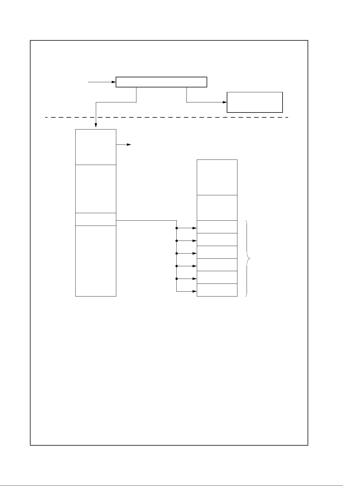
www.national.com 76 Revision 4.1
Functional Description (Continued)
Geode™ CS5530
Figure 3-7. General Purpose Timer and UDEF Trap SMI Tree Example
SMI# Asserted SMM s oftware reads SMI Header
If Bit X = 0
(Internal SMI)
If Bit X = 1
(External SMI)
Call internal SMI handler
to take appropriate action
Geode™ CS5530
F1BAR+Memory
Read to Clear
to determine
top-level source
of SMI
F1BAR+Memory
Offset 06h
Read to Clear
Bits [15:10]
Bits [8:0]
Bit 9
GTMR_TRP_SMI
Offset 02h
Geode™
to determine
second-level
source of SMI
Bit 5
PCI_TRP_SMI
Bit 4
UDEF3_TRP_SMI
Bit 3
UDEF2_TRP_SMI
Bit 2
UDEF1_TRP_SMI
Bit 1
GPT2_SMI
Bit 0
GPT1_SMI
Take
Appropriate
Action
Other_SMI
Other_SMI
If bit 9 = 1,
Source of SMI
is GP Timer or UDEF Trap
Bits 15: 6
RSVD
Top Level Second Level
SMI Deasserted after all SMI So urces are Cleared
(i.e., Top and Second Levels - note some sources may have a Third Level)
GXLV
Processor

Revision 4.1 77 www.national.com
Functional Description (Continued)
Geode™ CS5530
T able 3-32. Top Level SMI Status Register (Read to Clear)
Bit Description
F1BAR+Memory Offset 02h-03h Top Level SMI Status Register (RC) Reset Value = 0000h
15 Suspend Modulation Enable Mirror (Read to Clear): This bit mirrors the Suspend M odulation Feature Enable bit (F0
Index 96h[0]). It is us ed by the SMI handler to determine if the SMI Speedup Disable Register (F1BAR+Memor y Offset
08h) must be cleared on exit.
14 SMI Source is US B (Read to Clear): SMI was caused by USB activity? 0 = No; 1 = Yes.
SMI generation is configured in F0 Index 42h[7:6].
13 SMI Source is Warm Reset Command (Read to Clear): SMI was caused by Warm Reset command?
0=No;1=Yes.
12 SMI Source is NMI (Read to Clear): SMI was caused by NMI activity ? 0 = No; 1 = Yes.
11:10 Reserved (Read to Clear): Always reads 0.
9 SMI Source is G eneral Purpose Timers/User Defined Device Traps/Register Space Trap (Read to Clear): SMI was
caused by expiration of GP Timer 1/2; trapped access to UDEF3/2/1; t rapped access to F1-F4 or ISA Legacy Register
Space? 0 = No; 1 = Yes.
The next level of status is found at F1BAR+Memor y Offset 04h/06h.
8 SMI Source is Software Generated (Read to Cl ear): SMI was caused by software? 0 = No; 1 = Yes.
7 SMI on an A20M# Toggle (Read to Clear): SMI was caused by an access to either Port 092h or the keyboard command
which initiates an A20M# SMI? 0 = No; 1 = Yes.
This method of controlling the internal A20M# in the GXLV processor is used instead of a pin.
SMI generation enabling is at F0 Index 53h [0].
6 SMI Source is a VGA Timer Event (Read to Clear): SMI was caused by the expiration of the VGA Timer
(F0 Index 8 Eh)? 0 = No; 1 = Yes.
SMI generation enabling is at F0 Index 83h [3].
5 SMI Source is Video Retrace (IRQ2) (Read to Clear): SMI was caused by a video retrace event as decoded from the
serial connection (PSERIAL register, bit 7) from the GXLV processor? 0 = No; 1 = Yes.
SMI generation enabling is at F0 Index 83h [2].
4:2 Reserved (Read to Clear): Always reads 0.
1 SMI Source is Audio Interface (Read to Clear): SMI was caused by the audio interface? 0 = No; 1 = Yes.
The next level SMI status registers is found in F3BAR+Memory Offset 10h/12h.
0 SMI Source i s Power Management Event (Read to Clear): SMI was caused by one of the power management
resources? 0 = No; 1 = Yes.
The next level of status is found at F0 Index 84h-87h/F4h-F7h.
Note: The status for the General Purpose Timers andthe User Device Defined Traps are checked separately in bit 9.
Note: Reading this register clears all the SMI status bits. Note that bits 9, 1, and 0 h ave another level (second) of status reporting.
A read-only “Mirror ” version of this register exists at F1BAR+Memory Offset 00h. If the value of the registe r must be read without clearing the SMI source (and consequently deasserting SMI), the Mirror register may be readinstead.

www.national.com 78 Revision 4.1
Functional Description (Continued)
Geode™ CS5530
Table 3-33. Second Level Pwr Mgmnt SMI Status Reporting Registers (Read to Clear)
Bit Description
F1BAR+Memory Offset 06h-07h Second Level General Traps/Timers Reset Value = 0000h
SMI Status Register (RC)
15:6 Reserved (Read to Clear)
5 PCI Function Trap (Read to Clear): SMI was caused by a trapped configuration cycle (listed below)?
0=No;1=Yes.
This is the second level of SMI status report ing. The top level is r eported in F1BAR+Memor y Offset 00h/02h[9].
Trapped Access to F 1 Register Space; SMI generation enabling is at F0 Index 41h[3].
Trapped Access to F 2 Register Space; SMI generation enabling is at F0 Index 41h[6].
Trapped Access to F 3 Register Space; SMI generation enabling is at F0 Index 42h[0].
Trapped Access to F 4 Register Space; SMI generation enabling is at F0 Index 42h[1].
Trapped Access to I SA Legacy I/O Register Space; SMI generation enabling is at F0 Index 41h[0].
4 SMI Source is Trapped Access to User Defined Device 3 (Read to Clear): SMI was caused by a t rapped I/O o r mem-
ory access to the User Defined Device 3 (F0 Index C8h)? 0 = No; 1 = Yes.
This is the second level of SMI status report ing. The top level is r eported in F1BAR+Memor y Offset 00h/02h[9].
SMI generation enabling is at F0 Index 82h [6].
3 SMI Source is Trapped Access to User Defined Device 2 (Read to Clear): SMI was caused by a t rapped I/O o r mem-
ory access to the User Defined Device 2 (F0 Index C4h)? 0 = No; 1 = Yes.
This is the second level of SMI status report ing. The top level is r eported in F1BAR+Memor y Offset 00h/02h[9].
SMI generation enabling is at F0 Index 82h [5].
2 SMI Source is Trapped Access to User Defined Device 1 (Read to Clear): SMI was caused by a t rapped I/O o r mem-
ory access to the User Defined Device 1 (F0 Index C0h)? 0 = No; 1 = Yes.
This is the second level of SMI status report ing. The top level is r eported in F1BAR+Memor y Offset 00h/02h[9].
SMI generation enabling is at F0 Index 82h [4].
1 SMI Source is Expired General Purpose Timer 2 (Read to Clear): SMI was caused by the expiration of General
Purpose Timer 2 (F0 Index 8Ah)? 0 = No; 1 = Yes.
This is the second level of SMI status report ing. The top level is r eported in F1BAR+Memor y Offset 00h/02h[9].
SMI generation enabling is at F0 Index 83h [1].
0 SMI Source is Expired General Purpose Timer 1 (Read to Clear): SMI was caused by the expiration of General
Purpose Timer 1 (F0 Index 88h)? 0 = No; 1 = Yes.
This is the second level of SMI status report ing. The top level is r eported in F1BAR+Memor y Offset 00h/02h[9].
SMI generation enabling is at F0 Index 83h [0].
Note: Reading this register clears all the SMI status bits.
A read-only “Mirror ” version of this register exists at F1BAR+Memory Offset 04h. If the value of the registe r must be read without clearing the SMI source (and consequently deasserting SMI), the Mirror register may be readinstead.

Revision 4.1 79 www.national.com
Functional Description (Continued)
Geode™ CS5530
F0 Index F4h Seco nd Level Power Management Status R eg ister 1 (RC) Reset Value = 00h
7:5 Reserved
4 Game Port SMI Status (Read to Clear): SMI was caused by a R/W access to game port (I/O Port 200h and 201h)?
0=No;1=Yes.
This is the second level of SMI status report ing. The top level is r eported in F1BAR+Memor y Offset 00h/02h[0].
Game Port Read SMI generation enabling is at F0 Index 83h[4].
Game Port Write SMI generation enabling is at F0 Index 53h[3].
3 GPIO7 SMI Status (Read to Clear): SMI was caused by transition on (properly-configured) GPIO7 pin?
0=No;1=Yes.
This is the second level of SMI status report ing. The top level is r eported in F1BAR+Memor y Offset 00h/02h[0].
SMI generation enabling is at F0 Index 97h [3].
2 GPIO5 SMI Status (Read to Clear): SMI was caused by transition on (properly-configured) GPIO5 pin?
0=No;1=Yes.
This is the second level of SMI status report ing. The top level is r eported in F1BAR+Memor y Offset 00h/02h[0].
SMI generation enabling is at F0 Index 97h [2].
1 GPIO4 SMI Status (Read to Clear): SMI was caused by transition on (properly-configured) GPIO4 pin?
0=No;1=Yes.
This is the second level of SMI status report ing. The top level is r eported in F1BAR+Memor y Offset 00h/02h[0].
SMI generation enabling is at F0 Index 97h [1].
0 GPIO3 SMI Status (Read to Clear): SMI was caused by transition on (properly-configured) GPIO3 pin?
0=No;1=Yes.
This is the second level of SMI status report ing. The top level is r eported in F1BAR+Memor y Offset 00h/02h[0].
SMI generation enabling is at F0 Index 97h [0].
Note: Proper ly-configured means that the GPIO pin must be enabled as a GPIO, an input, and to cause an SMI.
This register provides status on various power-management SMI events. Reading this register clears the SMI status bits. A
read-only (mirror) version of this register exists at F0 Index 84h.
Table 3-33. Second Level Pwr Mgmnt SMI Status Reporting Registers (Read to Clear) (Continued)
Bit Description

www.national.com 80 Revision 4.1
Functional Description (Continued)
Geode™ CS5530
F0 Index F5h Seco nd Level Power Management Status R eg ister 2 (RC) Reset Value = 00h
7 Video Idle Timer SMI Status (Read to Clear): SMI was caused by expiration of the Video Idle Timer Count Register (F0
Index A6h)? 0 = No; 1 = Yes.
This is the second level of SMI status report ing. The top level is r eported in F1BAR+Memor y Offset 00h/02h[0].
SMI generation enabling is at F0 Index 81h [7].
6 User Defined Device 3 (UDEF3) Idle Timer SMI Status (Read to Clear): SMI was caused by expiration of the UDEF3
Idle Timer Count Register (F0 Index A4h)? 0 = No; 1 = Yes.
This is the second level of SMI status report ing. The top level is r eported in F1BAR+Memor y Offset 00h/02h[0].
SMI generation enabling is at F0 Index 81h [6].
5 User Defined Device 2 (UDEF2) Idle Timer SMI Status (Read to Clear): SMI was caused by expiration of the UDEF2
Idle Timer Count Register (F0 Index A2h)? 0 = No; 1 = Yes.
This is the second level of SMI status report ing. The top level is r eported in F1BAR+Memor y Offset 00h/02h[0].
SMI generation enabling is at F0 Index 81h [5].
4 User Defined Device 1 (UDEF1) Idle Timer SMI Status (Read to Clear): SMI was caused by expiration of the UDEF1
Idle Timer Count Register (F0 Index A0h)? 0 = No; 1 = Yes.
This is the second level of SMI status report ing. The top level is r eported in F1BAR+Memor y Offset 00h/02h[0].
SMI generation enabling is at F0 Index 81h [4].
3 Keyboard/Mouse Idle Timer SMI Status (Read to Clear): SMI was caused by expiration of the Keyboard/Mouse Idle
Timer Count Register (F0 Index 9Eh)? 0 = No; 1 = Yes.
This is the second level of SMI status report ing. The top level is r eported in F1BAR+Memor y Offset 00h/02h[0].
SMI generation enabling is at F0 Index 81h [3].
2 Parallel/Serial Idle Tim er SMI Status (Read to Clear): SMI was caused by expiration of the Parallel/Serial Port Idle
Timer Count Register (F0 Index 9Ch)? 0 = No; 1 = Yes.
This is the second level of SMI status report ing. The top level is r eported in F1BAR+Memor y Offset 00h/02h[0].
SMI generation enabling is at F0 Index 81h [2].
1 Floppy Disk Idle Timer SMI Statu s (Read to Clear): SMI was caused by expiration of the Floppy Disk Idle Timer Count
Register (F0 Index 9Ah)? 0 = No; 1 = Yes.
This is the second level of SMI status report ing. The top level is r eported in F1BAR+Memor y Offset 00h/02h[0].
SMI generation enabling is at F0 Index 81h [1].
0 Primary Hard Disk Idle Timer SMI Status (Read to Clear): SMI was caused by expiration of the Pr imary Hard Disk Idle
Timer Count Register (F0 Index 98h)? 0 = No; 1 = Yes.
This is the second level of SMI status report ing. The top level is r eported in F1BAR+Memor y Offset 00h/02h[0].
SMI generation enabling is at F0 Index 81h [0].
Note: This register provides status on the Device Idle Timers to the SMI handler. A bit set here indicates that t he device was idle for
the duration configured in the Idle Timer Count register for that device, causing an SMI. Reading this register clears the SMI
status bits. A read-only (mirror) version of this register exists at F0 Index 85h. If the value of the register must be read wit hout
clearing the SMI source (and consequent ly deasserting SMI), F0 Index 85h may be read inst ead.
Table 3-33. Second Level Pwr Mgmnt SMI Status Reporting Registers (Read to Clear) (Continued)
Bit Description

Revision 4.1 81 www.national.com
Functional Description (Continued)
Geode™ CS5530
F0 Index F6h Seco nd Level Power Management Status R eg ister 3 (RC) Reset Value = 00h
7 Video Access Trap SMI Status (Read to Clear): SMI was caused by a trapped I/O access to the Video I/O Trap? 0 =
No; 1 = Yes.
This is the second level of SMI status report ing. The top level is r eported in F1BAR+Memor y Offset 00h/02h[0].
SMI generation enabling is at F0 Index 82h [7].
6 Reserved (Read Only)
5 Secondary Hard Disk Access Trap SMI Status (Read to Clear): SMI was caused by a trapped I/O access to the
secondary hard disk? 0 = No; 1 = Yes.
This is the second level of SMI status report ing. The top level is r eported in F1BAR+Memor y Offset 00h/02h[0].
SMI generation enabling is at F0 Index 83h [6].
4 Secondary Hard Disk Idle Timer SMI Status (Read to Clear): SMI was caused by expiration of the Hard Disk Idle
Timer Count Register (F0 Index ACh)? 0 = No; 1 = Yes.
This is the second level of SMI status report ing. The top level is r eported in F1BAR+Memor y Offset 00h/02h[0].
SMI generation enabling is at F0 Index 83h [7].
3 Keyboard/Mouse Access Trap SMI Status (Read to Clear): SMI wa s caused by a trapped I/O access to the keyboard
or mouse? 0 = No; 1 = Yes.
This is the second level of SMI status report ing. The top level is reported in F1BAR+Memory Offset 00h/02h[0].
SMI generation enabling is at F0 Index 82h [3].
2 Parallel/Serial Access TrapSMI Statu s (Read to Clear): SMI was caused by a trapped I/O access to either the serial or
parallel ports? 0 = No; 1 = Yes.
This is the second level of SMI status report ing. The top level is r eported in F1BAR+Memor y Offset 00h/02h[0].
SMI generation enabling is at F0 Index 82h [2].
1 Floppy Di sk Access Trap SMI Status (Read to Cl ear): SMI was caused by a trapped I/O access to the
floppy disk? 0 = No; 1 = Yes.
This is the second level of SMI status report ing. The top level is r eported in F1BAR+Memor y Offset 00h/02h[0].
SMI generation enabling is at F0 Index 82h [1].
0 Primary Hard Disk Access Trap SMI Statu s (Read to Clear): SMI was caused by a trapped I/O access to the
primary hard disk? 0= No; 1 = Yes.
This is the second level of SMI status report ing. The top level is r eported in F1BAR+Memor y Offset 00h/02h[0].
SMI generation enabling is at F0 Index 82h [0].
Note: This registerprovides status on the Device Trapsto the SMI handler. A bit set here indicates that an access occ u rred to the
device while the trapwas enabled, causing an SMI. Reading this register clears t he SMI status bits. A read-only (mirror) version of this register exists at F0 Index 86h. If the value of the register must be read without clearing the SMI source (and consequently deasserting SMI), F0 I ndex 86h may be read instead.
Table 3-33. Second Level Pwr Mgmnt SMI Status Reporting Registers (Read to Clear) (Continued)
Bit Description

www.national.com 82 Revision 4.1
Functional Description (Continued)
Geode™ CS5530
3.4.3.6 Device Power Management Register Programming Summary
Table 3-34 provides a programming register summary of
the deviceidle timers, address traps, and general purpose
I/O pins. For complete bit information regarding the registers listed in Table 3-34, refer to Section 4.3.1 “Bridge
Configuration Registers - Function 0” on page 149 and
Section 4.3.2 “SMI Status and ACPI Timer Registers Function 1” on page 179.
F0 Index F7h Second L evel Power Management Status Register 4 (RO/RC) Reset Value = 00h
7 GPIO2 SMI Status (Read to Clear): SMI was caused by transition on (properly-configured) GPIO2 pin?
0=No;1=Yes.
This is the second level of SMI status report ing. The top level is r eported in F1BAR+Memor y Offset 00h/02h[0].
SMI generation enabling is at F0 Index 92h [2].
6 GPIO1 SMI Status (Read to Clear): SMI was caused by transition on (properly-configured) GPIO1 pin?
0=No;1=Yes.
This is the second level of SMI status report ing. The top level is r eported in F1BAR+Memor y Offset 00h/02h[0].
SMI generation enabling is at F0 Index 92h [1].
5 GPIO0 SMI Status (Read to Clear): SMI was caused by transition on (properly-configured) GPIO0 pin?
0=No;1=Yes.
This is the second level of SMI status report ing. The top level is r eported in F1BAR+Memor y Offset 00h/02h[0].
SMI generation enabling is at F0 Index 92h [0].
4 Lid Position (Read Only): This bit maintains the current status of the lid position. If the GPIO6 pin is configured as the lid
switch indicator, this bit reflects the state of the pin.
3 Lid Switch SMI Status (Read to Clear): SMI was caused by a transition on the GPIO6 (lid switch) pin?
0=No;1=Yes.
For this to happen, the G PIO6 pin must be configured both as an input (F0 Index 90h[6] = 0) and as the lid switch (F0
Index 92h[6] =1).
2 Codec SDATA_IN SMI Status (Read to Clear): SMI was caused by an AC97 codec producing a positive edge on
SDATA_IN? 0 = No; 1 = Yes.
This is the second level of status is reporting. The top level status is reported in F1BAR+Memor y Offset 00h/02h[0].
SMI generation enabling is at F0 Index 80h [5].
1 RTC Alarm (IRQ8) SMI Status (Read to Clear): SMI was caused by an RTC interrupt? 0 = No; 1 = Yes.
This SMI event can only occur while in 3V Suspend and RTC interrupt occurs.
This is the second level of SMI status report ing. The top level is r eported in F1BAR+Memor y Offset 00h/02h[0].
0 ACPI Timer SMI Status (Read to Clear): SMI was caused by an ACPI Timer MSB toggle? 0 = No; 1 = Yes.
This is the second level of SMI status report ing. The top level is r eported in F1BAR+Memor y Offset 00h/02h[0].
SMI generation configuration is at F0 Index 83h[5].
Note: Proper ly-configured means that the GPIO pin must be enabled as a GPIO, an input, and to cause an SMI.
This register provides status on several miscellaneous power management events that generate SMIs, as well as the status of
the Lid Switch. Reading this register clears the SMI status bits. A read-only (mirror) version of this register exists at F0 Index
87h.
Table 3-33. Second Level Pwr Mgmnt SMI Status Reporting Registers (Read to Clear) (Continued)
Bit Description

Revision 4.1 83 www.national.com
Functional Description (Continued)
Geode™ CS5530
Table 3-34. Device Power Management Programming Summary
Device Power
Management Resource
Located at F0 Index xxh Unless Otherwise No ted
Enable Configuration
Second Level
SMI Status/No Clear
Second Level SMI
Status/With Clear
Global Timer Enable 80h[1] N/A N/A N/A
Keyboard / Mouse Idle Timer 81h[3] 93h[1:0] 85h[3] F5h[3]
Parallel / Serial Idle Timer 81h[2] 93h[1:0] 85h[2] F5h[2]
Floppy Disk Idle Timer 81h[1] 9Ah[15:0], 93h[7] 85h[1] F5h[1]
Video Idle Timer (Note 1) 81h[7] A6h[15:0] 85h[7] F5h[7]
VGA Timer (Note 2) 83h[3] 8Eh[7:0] F1BAR+Memory
Offset 00h[6]
F1BAR+Memory
Offset 02h[6]
Primary Hard Disk I dle T imer 81h[0] 98h[15:0], 93h[5] 85h[0] F5h[0]
Secondary Hard Disk Idle Timer 83h[7] ACh[15:0], 93h[4] 86h[4] F6h[4]
User Defined Device 1 Idle Timer 81h[4] A0h[15:0], C0h[31:0],
CCh[7:0]
85h[4] F5h[4]
User Defined Device 2 Idle Timer 81h[5] A2h[15:0], C4h[31:0],
CDh[7:0]
85h[5] F5h[5]
User Defined Device 3 Idle Timer 81h[6] A4h[15:0], C8h[31:0],
CEh[7:0]
85h[6] F5h[6]
Global Trap Enable 80h[2] N/A N/A N/A
Keyboard / Mouse Trap 82h[3] 9Eh[15:0] 93h[1:0] 86h[3] F6h[3]
Parallel / Serial Trap 82h[2] 9Ch[15:0], 93h[1:0] 86h[2] F6h[2]
Floppy Disk Trap 82h[1] 93h[7] 86h[1] F6h[1]
Video Access Trap 82h[7] N/A 86h[7] F6h[7]
Primary Hard Disk Trap 82h[0] 93h[5] 86h[0] F6h[0]
Secondary Hard Disk Trap 83h[6] 93h[4] 86h[5] F6h[5]
User Defined Device 1 Trap 82h[4] C0h[31:0], CCh[7:0] F1BAR+Memory
Offset 04h[2]
F1BAR+Memory
Offset 06h[2]
User Defined Device 2 Trap 82h[5] C4h[31:0], CDh[7:0] F1BAR+Memory
Offset 04h[3]
F1BAR+Memory
Offset 06h[3]
User Defined Device 3 Trap 82h[6] C8h[31:0], CEh[7:0] F1BAR+Memory
Offset 04h[4]
F1BAR+Memory
Offset 06h[4]
General Purpose Timer 1 83h[0] 88h[7:0], 89h[7:0], 8Bh[ 4] F1BAR+Memory
Offset 04h[0]
F1BAR+Memory
Offset 06h[0]
General Purpose Timer 2 83h[1] 8Ah[7:0], 8B h[5,3,2] F1BAR+Mem ory
Offset 04h[1]
F1BAR+Memory
Offset 06h[1]
GPIO7 Pin N/A 90h[7], 91h[7], 92h[7],
97h[7,3]
91h[7] N/A
GPIO6 Pin N/A 90h[6], 91h[6], 92h[6] 87h[ 4,3], 91h[6] F7h[4,3]
GPIO5 Pin N/A 90h[5], 91h[5], 97h[6,2] 91h[5] N/A
GPIO4 Pin N/A 90h[4], 91h[4], 97h[5,1] 91h[4] N/A
GPIO3 Pin N/A 90h[3], 91h[3], 97h[4,0] 91h[3] N/A
GPIO2 Pin N/A 90h[2], 91h[2], 92h[5,2] 87h[7], 91h[2] F7h[7]
GPIO1 Pin N/A 90h[1], 91h[1] 92h[4,1] 87h[6], 91h[1] F7h[6]
GPIO0 Pin N/A 90h[0], 91h[0], 92h[3,0] 87h[5], 91h[0] F7h[5]
Suspend Modulation OFF/ON
Video Speedup
IRQ Speedup
96h[0]
80h[4]
80h[3]
94h[7:0]/95h[7:0]
8Dh[7:0]
8Ch[7:0]
N/A
A8h[15:0]
N/A
N/A
N/A
N/A
Note: 1. This functionis used for Suspend determination.
2. This function is used for SoftVGA.

www.national.com 84 Revision 4.1
Functional Description (Continued)
Geode™ CS5530
3.5 PC/AT COMPATIBILITY LOGIC
The CS5530’s PC/AT compatibility logic provides support
for the standard PC architecture. This subsystem also
provides legacy support for existing hardware and software. Support functions for the GXLV processor provided
by these subsystems include:
• ISA Subtractive Decode
• ISA Bus Interface
- Delayed PCI Transactions
- Limited ISA and ISA Master Modes
• ROMInterface
• Megacells
- Direct Memory Access (DMA)
- Programmable Interval Timer
- Programmable Interrupt Controller
- PCI Compatible Interrupts
- System Control I/O Port 092h and061h
- Keyboard Interface Function
- External Real-Time Clock Interface
The following subsections give a detailed description for
each of these functions.
3.5.1 ISA Subtractive Decode
The CS5530 provides an ISA bus controller. The CS5530
is the default subtractive-decoding agent, and forwards all
unclaimed memory and I/O cycles to the ISA interface.
However, the CS5530 can be configured using F0 Index
04h[1:0] to ignore either I/O, memory, or all unclaimed
cycles (subtractive decode disabled, F0 Index 41h[2:1] =
1x (Table 3-35).
Table 3-35. Cycle Configuration Bits
Bit Description
F0 Index 04h-05h PCI Com mand Register (R/W) Reset Value = 0000h
1 Memory Space: Allow the CS5530 to respond to memory cycles from the PCI bus:
0 = Disable; 1 = Enable (Default).
0 I/O Space: Allow the CS5530 to respond to I/O cycles f rom the PCI bus: 0 = Disable; 1 = Enable (Default).
F0 Index 41h PCI Function Control Register 2 (R/W) Reset Val ue = 10h
2:1 Subtractive Decode: These bits determine the point at which the CS5530 accepts cycles that are not claimed by another
device. The CS5530 defaults to taking subtractive decode cycles in the default cycle clock, but can be moved up to the
Slow Decode cycle point if all other PCI devices decode in the fast or medium clocks. Disabling subtractive decode must
be done with care, as all ISA and ROM cycles are decoded subtractively.
00 = Default sample (4th clock from FRAME# active)
01 = Slow sample (3rd clock from FRAME# active)
1x = No subtractive decode

Revision 4.1 85 www.national.com
Functional Description (Continued)
Geode™ CS5530
3.5.2 ISA B us Interface
The ISA bus controller issues multiple ISA cycles to satisfy PCI transactions that are largerthan 16 bits. A full32bit read or write results in two 16-bit ISA transactions or
four 8-bit ISA transactions. The ISA controller gathers the
data from multiple ISA read cycles and returns TRDY#
only after all of the data can be presented to the PCI bus
at the same time.
SA[23:0] are a concatenation of ISA LA[23:17] and
SA[19:0] and perform equivalent functionality at a reduced
pin count.
Figure 3-8 shows the relationship between a PCI cycle
and the corresponding ISA cycle generated.
Figure 3-8. Non-Posted PCI-to-ISA Access
PCI_CLK
ISACLK
FRAME#
IRDY#
TRDY#
AD[31:0] (Read)
IOR#/IOW#
AD[31:0] (Write)
BALE
STOP#
MEMR#/MEMW#

www.national.com 86 Revision 4.1
Functional Description (Continued)
Geode™ CS5530
3.5.2.1 Delayed PCI Transactions
If PCI delayed transactions are enabled (F0 Index 42h[5]
= 1) multiple PCI cycles occur for every slower ISA cycle.
Figure 3-9 shows the relationship of PCI cycles to an ISA
cycle with PCI delayed transactions enabled.
See Section 3.2.6 “Delayed Transactions” on page 48 for
additional information.
Figure 3-9. PCI to ISA Cycles with Delayed Transaction Enabled
REQ#
GNT#
FRAME#
IRDY#
TRDY#
STOP#
IOR#
BALE
PCI
1
1
1
1
1-Delay
2
3
2 - IDE bus master - starts and completes
3 - End of ISA cycle
ISA

Revision 4.1 87 www.national.com
Functional Description (Continued)
Geode™ CS5530
3.5.2.2 Limited ISA and ISA Master Modes
The CS5530 supports two modes on the ISA interface.
The default mode of the ISA bus is a fully functional ISA
mode, but it does not suppor t ISA masters, as shown in
Figure 3-10 “Limited ISA Mode”. When in this mode, the
address and data buses are multiplexed together, requiringanexternallatchtolatchthelower16bitsofaddress
of the ISA cycle. The signal SA_LATCH is generated
when the data on the SA/SD bus is a valid address. Additionally, the upper four address bits, SA[23:20], are multiplexed on GPIO[7:4].
The second mode of the ISA interface supports ISA bus
masters, as shown in Figure 3-11. When the CS5530 is
placed in the ISA Master mode, a large number of pins
are redefined as shown in Table 3-36.
In this mode of operation, the CS5530 cannot support
TFT flat panels or TV controllers, since most of the signals
used to support these functions havebeen redefined. This
mode is required if ISA slots or ISA masters are used. ISA
master cycles are only passed to the PCI bus if they
access memory. I/O accesses are left to complete on the
ISA bus. SA[15:0] and MASTER# are not 5.0V tolerant;
therefore, the SA lines require a buffer and MASTER#
should be pulled up to 3.3V (not 5.0V).
The mode of operation is selected by the strapping of pin
P26 (INTR):
• ISALimitedMode—StrappinP26(INTR)lowthrough
a 10-kohm resistor.
• ISAMaster Mode — Strap pin P26 (INTR) high through
a 10-kohm resistor.
Bit 7 of F0 Index 44h[7] (bit details on page 152) reports
thestrapvalueoftheINTRpin(pinP26)duringPOR:0=
ISA Limited; 1 = ISA Master.
This bit can be written after POR# deassertion to change
the ISA mode selected. Writing to this bit is not recommended due to the actual strapping done on the board.
ISA memory and ISA refresh cycles are not supported by
the CS5530. Although, the refresh toggle bit in I/O Port
061h still exists for software compatibility reasons.
Note: If Limited ISA Mode of operation has been
selected, SMEMW# and SMEMR# can be output
on these pins by programming F0 Index 53[2] = 0
(bit details on page 154).
Table 3-36. Signal Assignments
Pin No. Limited ISA Mode
ISA Master
Mode
AD15 SA_LATCH SA_DIR
AE25, AD24,
AE22, AE21,
AF21, AC20,
AD19, AF19,
AF4, AF5,
AD5, AF6,
AC6, AD9,
AE6, AE9
SA[15:0]/SD[15:0] SD[15:0]
H2, K1, K2,
L1, D1, E2,
F1, G1, G3,
G4, G2, H1,
J1,J3,J2,K3
FP_DATA[15:0] SA[15:0]
H3 FP_DATA[16] SA_OE#
F3 FP_DATA[17] MASTER#
E1 FP_HSYNC_OUT SMEMW#
E3 FP_VSYNC_OUT SMEMR#
AF3 (Note) SMEMW# RTCCS#
AD4 (Note)SMEMR# RTCALE
AF23, AE23,
AC21, AD22
GPIO[7:4]
SA[23:20]
SA[23:20]

www.national.com 88 Revision 4.1
Functional Description (Continued)
Geode™ CS5530
Figure 3-10. Limited ISA Mode
Figure 3-11. ISA Master Mode
Notes:
1. F0 Index 43h[2] controls GPIO[7:4]/SA[23:20].
2. These signals are: MEMW#, MEMR#, IOR#, IOW#, T C, AEN, DREQ[7:5, 3:0], DACK[7:5, 3:0]#, MEMCS16#, ZEROWS#,
SBHE#, IOCS16#, IOCHRDY, ISACLK.
3. This resistor is used at boot time to determine the mode of the ISA bus.
QD
ISA Control
2
SD[15:0]
SA[23:20]
SA[19:16]
SA[15:0]
1
GPIO[7:4]/SA[23:20]
SA[19:16]
SA[15:0]/SD[15:0]
SA_LATCH/SA_DIR
10K
3
74F373x2
G
OC
ISA Device
Geode™
INTR
CS5530
BA
ISA Control
2
SMEMW#
MASTER#
SA[23:20]
SA[19:16]
FP_VSYNC_OUT/SMEMR#
1
GPIO[7:4]/SA[23:20]
SA[19:16]
FP_DATA16/SA_OE#
SA_DIR
10K
3
74L245x2
OE#
T/R
ISA Master
SMEMR#
FP_HSYNC_OUT/SMEMW#
FP_DATA17/MASTER#
FP_DATA[15:0]/SA[15:0] SA[15:0]
SA_LATCH/SA_DIR
SA_OE#
SA[15:0]_SD[15:0]/SD[15:0] SD[15:0]
Geode™
Notes:
1. When st rapped for ISA Master mode, GPIO[7:4]/SA[23:20] are set to SA[23:20] and the settings in F0 Index 43h[2] ar e invalid.
2. These signals are: MEMW#, MEMR#, IOR#, IOW#, T C, AEN, DREQ[7:5, 3:0], DACK[7:5, 3:0]#, MEMCS16#, ZEROWS#,
SBHE#, IOCS16#, IOCHRDY, ISACLK.
3. This resistor is used at boot time to deter mine the mode of the ISA bus.
INTR
5.0V
3.3V
330Ω
CS5530

Revision 4.1 89 www.national.com
Functional Description (Continued)
Geode™ CS5530
3.5.2.3 ISA Bus Data Steering
TheCS5530performsalloftherequireddatasteering
from SD[7:0] to SD[15:0] during normal 8-bit ISA cycles,
as well as during DMA and ISA master cycles. It handles
data transfers between the 32-bit PCI data bus and the
ISA bus. 8/16-bit devices can reside on the ISA bus. Various PC-compatibleI/O registers, DMA controller registers,
interrupt controller registers, and counter/timer registers
lie on the on-chip I/O data bus. Either the PCI bus master
ortheDMAcontrollerscanbecomethebusowner.
When the PCI bus master is the bus owner, the CS5530
data steering logic provides data conversion necessary
for 8/16/32-bit transfers to and from 8/16-bit devices on
either the ISA bus or the 8-bit registers on the on-chip I/O
data bus. When PCI data bus drivers of the CS5530 are
tristated, data transfers between the PCI bus master and
PCI bus devicesare handled directly via the PC I data bus.
When the DMA requestor is the bus owner, the CS5530
allows 8/16-bit data transfer between the ISA bus and the
PCI data bus.
3.5.2.4 I/O Recovery Delays
In normal operation, the CS5530 i nserts a delay between
back-to-back ISA I/O cycles that or i ginate on the PCI bus.
The default delay is four ISACLK cycles. Thus, the second
of consecutive I/O cycles is held in the ISA bus controller
until this delay count has expired. The delay is measured
between the rising edge of IOR#/IOW# and the falling
edge of BALE. This delay can be adjusted to a greater
delay through the ISA I/O Recovery Control Register (F0
Index 51h, see Table 3-37).
Note: This delay is not inserted for a 16-bit ISA I/O
access that is split into two 8-bit I/O accesses.
Table 3-37. I/O Recovery Programming Register
Bit Description
F0 Index 51h ISA I/O Recovery Control Register (R /W) Reset Value = 44h
7:4 8-Bit I/O Recovery: These bits determine the number of ISA bus clocks between back-to-back 8-bit I/O read cycles. This
count is in addition to a preset one-clock delay built int o t he controller.
0000 = 1 PCI clock 0100= 5 PCI clocks 1000 =9 PCI clocks 1100 = 13 PCI clocks
0001 = 2 PCI clocks 0101 = 6 PCI clocks 1001 =10 PCI clocks 1101 = 14 PCI clocks
0010 = 3 PCI clocks 0110 = 7 PCI clocks 1010 =11 PCI clocks 1110 = 15 PCI clocks
0011 = 4 PCI clocks 0111 = 8 PCI clocks 1011 =12 PCI clocks 1111 = 16 PCI clocks
3:0 16-Bit I/O Recovery: These bits determine the number of ISAbus clocks between back-to-back 16- bit I/O cycles. This
count is in addition to a preset one-clock delay built int o t he controller.
0000 = 1 PCI clock 0100= 5 PCI clocks 1000 =9 PCI clocks 1100 = 13 PCI clocks
0001 = 2 PCI clocks 0101 = 6 PCI clocks 1001 =10 PCI clocks 1101 = 14 PCI clocks
0010 = 3 PCI clocks 0110 = 7 PCI clocks 1010 =11 PCI clocks 1110 = 15 PCI clocks
0011 = 4 PCI clocks 0111 = 8 PCI clocks 1011 =12 PCI clocks 1111 = 16 PCI clocks

www.national.com 90 Revision 4.1
Functional Description (Continued)
Geode™ CS5530
3.5.2.5 ISA DMA
DMA transfers occur between ISA I/O peripherals and
system memor y. The datawidth can be either 8 or 16 bits.
Out of the seven DMA channels available, four are used
for 8-bit transfers while the remaining three are used for
16-bit transfers. One BYTE or WORD is transferred in
each DMA cycle.
Note: The CS5530does not support DMA transfers to
ISA memory.
The ISA DMA device initiates a DMA requestby asserting
oneoftheDRQ[7:5,3:0]signals.WhentheCS5530
receives this request, it sends a bus grant request to the
PCI arbiter. After the PCI bus has been granted, the
respectiveDACK#isdrivenactive.
The CS5530 generates PCI memory read or write cycles
in response to a DMA cycle. Figures 3-12 and 3-13 are
examplesof DMA memory read andmemory write cycles.
Upon detection of the DMA controller’s MEMR# or
MEMW#active,theCS5530startsthePCIcycle,asserts
FRAME#, and negates an internal IOCHRDY. This
assures the DMA cycle does not c omplete before the PCI
cycle has provided or accepted the data. IOCHRDY is
internally asserted when IRDY# and TRDY# are sampled
active.
Figure 3-12. ISA DMA Read from PCI Memory
Figure 3-13. ISA DMA Write To PCI Memory
PCICLK
ISACLK
MEMR#
IOW#
FRAME#
AD[31:0]
IRDY#
TRDY#
SD[15:0]
IOCHRDY
PCICLK
ISACLK
MEMW#
IOR#
FRAME#
AD[31:0]
IRDY#
TRDY#
SD[15:0]
IOCHRDY

Revision 4.1 91 www.national.com
Functional Description (Continued)
Geode™ CS5530
3.5.3 ROM Interface
The CS5530 positively decodes memory addresses
000F0000h-000FFFFFh (64 KB) and FFFC0000hFFFFFFFFh (256 KB) at reset. These memory cycles
cause the CS5530 to claim the cycle, and generate an
ISA bus memory cycle with KBROMCS# asserted. The
CS5530 can also be configured to respond to memory
addresses FF000000h-FFFFFFFFh (16 MB) and
000E0000h-000FFFFFh(128 KB).
Flash ROM is supported in the CS5530 by enabling the
KBROMCS# signal on write accesses to the ROM region.
Normally only read cycles are passed to the ISA bus, and
the KBROMCS# signal is suppressed. When the ROM
Write Enable bit (F0 Index 52h[1]) is set, a write accessto
the ROM address region causes an 8-bit write cycle to
occur with MEMW# and KBROMCS# asserted.
Table 3-38 shows the ROM interface related programming
bits.
3.5.4 Megacells
The CS5530 core logic integrates:
• Two 8237-equivalent DMA controllers (DMAC) with full
32-bit addressing for DMA transfers.
• Two 8259-equivalent interrupt controllers providing 13
individually programmable external interrupts.
• An 8254-equivalent timer for refresh, timer, and
speaker logic.
• NMI control and generation for PCI system errors and
all parity errors.
• Support for standard AT keyboard controllers, reset
control, and VSA technology audio.
Table 3-38. ROM Interface Related Bits
Bit Description
F0 Index 52h ROM/AT Logic Control Register (R/W) Reset Value = F8h
2 Upper ROM Address Range: KBROMCS# is asserted for ISA memor y read accesses:
0 = FFFC0000h-FFFFFFFFh (256 KB, Default); 1 = FF000000h-FFFFFFFFh (16 MB)
Note: PCI Positive decoding for the ROM space is enabled at F0 Index 5Bh[5]).
1 ROM Write Enable: Assert KBROMCS# during writes to configured ROM space (configured in bits 2 and 0),
allowing Flash programming:0 = Disable; 1 = Enable.
0 Lower ROM Address Range: KBROMCS# is asserted for ISA memory read accesses:
0 = 000F0000h-000FFFFFh (64 KB, Default); 1 = 000E0000h-000F F FFFh (128 KB).
Note: PCI Positive decoding for the ROM space is enabled at F0 Index 5Bh[5]).
F0 Index 5Bh Decode Control Register 2 (R/W) Reset Value = 2 0h
5 BIOS ROM Positive Decode: Selects PCI positive or subtractive decoding for accesses to the configured ROM space: 0
= Subtractive; 1 = Positive.
ROM configuration is at F0 Index 52h[2:0].

www.national.com 92 Revision 4.1
Functional Description (Continued)
Geode™ CS5530
3.5.4.1 Direct Memory Access (DMA)
The 8237-compatible DMA controllers on the CS5530
control transfers between ISA I/O devices and PCI or ISA
memory. They generate a bus request to the PCI bus
when an I/O device requests a DMA operation. Once they
are granted the bus, the DMA transfer cycle occurs. DMA
transferscan occur over the entire 32-bit address range of
the PCI bus.
The CS5530 contains registers for driving the high
address bits (high page) and registers for generating the
middle address bits (low page) output by the 8237 controller.
DMA Controllers
The CS5530 supports seven DMA channels using two
standard 8237-equivalent controllers. DMA Controller 1
contains Channels 0 through 3 and supports 8-bit I/O
adapters. These channels are used to transfer data
between8-bit peripherals and PCI memory or 8/16-bit ISA
memory. Using the high and low page address registers, a
full 32-bit PCI address is output for each channel so they
can all transfer data throughout the entire 4 GB system
address s pace. Each channel can transfer data in 64 KB
pages.
DMA Controller 2 contains Channels 4 through 7. Channel 4 is used to cascade DMA Controller 1, so it is not
availabl e externally. Channels 5 through 7 support 16-bit
I/O adapters to transfer data between 16-bit I/O adapters
and 16-bit system memory. Using the high and low page
address registers, a full 32-bit PCI address is output for
each channel so they can all transfer data throughout the
entire 4 GB system address space. Each channel can
transferdata in 128 KB pages. Channels 5, 6, and 7 transfer 16-bit words on even byte boundaries only.
DMA Transfer Modes
Each DMA channel can be programmed for single, bloc k,
demand or cascade transfer modes. In the most commonly used mode, single transfer mode, one DMA cycle
occurs per DRQ and the PCI bus is released after every
cycle. This allows the CS5530 to timeshare the PCI bus
with the CPU. This is imperative, especially in cases
involving large data transfers, because the CPU gets
locked out for too long.
In block transfer mode, the DMA controller executes all of
its transfers consecutively without releasing the PCI bus.
In demandtransfer mode, DMA transfercycles continue to
occur as long as DRQ is high or terminal count is not
reached. In this mode, the DMA controller continues to
execute transfer cycles until the I/O device drops DRQ to
indicate its inability to continue providing data. For this
case, the PCI bus is held by the CS5530 until a break in
the transfers occurs.
In cascade mode, the channel is connected to another
DMA controller or to an ISA bus master, rather than to an
I/O device. In the CS5530, one of the 8237 controllers is
designated as the master and the other as the slave. The
HOLD output of the slave is tied to the DRQ0 input of the
master (Channel 4), and the master’s DACK0# output is
tied to the slave’sHLDA input.
In each of these modes, the DMA controller can be programmed for read, write, or verify transfers.
Both DMA controllers are reset at Power On Reset (POR)
to fixed priority. Since master Channel 0 is actually connected to the slave DMA controller, the slave’s four DMA
channels have the highest priority, with Channel 0 as
highest and Channel 3 as the lowest. Immediately following slave Channel 3, master Channel 1 (Channel 5) is the
next highest, followed by Channels 6 and 7.
DMA Controller Registers
The DMA controller can be programmed with standard I/O
cycles to the standard register space for DMA. The I/O
addresses of all registers for the DMA controller are listed
in Table 4-25 "DMA Channel Control Registers" on page
208.
Addresses under Master are for the 16-bitDMA channels,
and Slave corresponds to the 8-bit channels. When writing to a channel's address or word-count register, the data
is written into both thebase register and the current register simultaneously. When reading a channel address or
word count register, only the current address or word
count can be read. The base address and base word
count are not accessible for reading.
DMA Transfer Types
Each of the seven DMA channels may be programmed to
perform one of three types of transfers: read, write, or verify.Thetransfertypeselecteddefinesthemethodusedto
transfera BYTEor WORD during one DMA buscycle.
For read transfer types, the CS5530 reads data from
memoryandwritesittotheI/Odeviceassociatedwiththe
DMA channel.
For write transfer types, the CS5530 reads data from the
I/O device associated with the DMA channel and wr ites to
the memory.
The verify transfer type causes the CS5530 to execute
DMA transfer bus cycles, including generation of memory
addresses, but neither the Read nor Write command lines
are activated. This transfer type was used by DMA Channel 0 to implement DRAM refresh in the original IBM
PC/XT™.
DMA Priority
The DMA controller may be programmed for two types of
priority schemes: fixed and rotate (I/O Ports 008h[4] and
0D0h[4], as shown in Table 4-25 "DMA Channel Control
Registers" on page 208.
In fixed priority, the channels are fixed in priority order
based on the descending values of their numbers. Thus,
Channel 0 has the highest priority. In rotate priority, the
last channel to get service becomes the lowest-priority

Revision 4.1 93 www.national.com
Functional Description (Continued)
Geode™ CS5530
channel with the priority of the others rotating accordingly.
This preventsa channel fromdominating the system.
The address and word count registers for each channel
are 16-bit registers. The value on the data bus is written
into the upper byte or lower byte, depending on the state
of the internal addressing byte pointer. This pointer can be
cleared by the Clear Byte Pointer command. After this
command, the first read/write to an address or word count
register will read/write to the low byte of the 16-bit register
and the byte pointer will point to the high byte. The next
read/write to an address or word-count register will read
or write to the high byte of the 16-bit register and the byte
pointer will point back to the lowbyte.
When programming the 16-bit channels (Channels 5, 6,
and 7), the address which is written to the base address
register must be the real addressdivided by two. Also, the
base word count for the 16-bit channels is the number of
16-bit words to be transferred, not the number of bytes as
is the case for the 8-bitchannels.
TheDMAcontrollerallowstheusertoprogramtheactive
level (low or high) of the DRQ and DACK# signals. Since
the two controllers are cascaded together internally on the
chip,these signals should alwaysbe programmed with the
DRQ signal active high and the DACK# signal active low.
DMA Shadow Registers
The CS5530 contains a shadow register located at F0
Index B8h (Table 3-39) for reading the configuration of the
DMA controllers. This read-only register can sequence to
read through all of theDMA registers.
DMA Addressing Capability
DMA transfers occur over the entire 32-bit address range
of the PCI bus. This is accomplished by using the DMA
controller’s 16-bit memory address registers in conjunction with an 8-bit DMA Low Page register and an 8-bit
DMA High Page register.These registers, associated with
each channel, provide the 32-bit memory address capability. A write to the Low Page register clears the High
Page register, for backward compatibility with the PC/AT
standard. The starting address for the DMA transfer must
be programmed into the DMA controller registers and the
channel’s respective Low and High Page registers prior to
beginning the DMA transfer.
DMA Page Registers and Extended Addressing
The DMA Page registers provide the upper address bits
during DMA cycles. DMA addresses do not increment or
decrement across page boundaries. Page boundaries for
the 8-bit channels (Channels 0 through 3) are every 64
KB and page boundaries for the 16-bit channels (Channels 5, 6, and 7) are every 128 KB.
Before any DMA operations are performed, the Page
Registers must be written at the I/O Port addresses
shown in Table 4-26 "DMA Page Registers" on page 211
to select the correct page for each DMA channel. The
other address locations between 080h and 08Fh and
480h and 48Fh are not used by the DMA channels, but
canbereadorwrittenbyaPCIbusmaster.Theseregisters are reset to zero at POR. A write to the Low Page
register clears the High Page register, for backward compatibility with the PC/AT standard.
For m ost DMA transfers, the High Page register is set to
zeros and is driven onto PCI address bits AD[31:24] during DMA cycles. This mode is backward compatible with
the PC/AT standard. For DMA extended transfers, the
High Page register is programmed and the values are
driven onto the PCI addresses AD[31:24] during DMA
cycles to allow access to the full 4 GB PCI address space.
DMA Address Generation
The DMA addresses are formed such that there is an
upper address, a middle address, and a lower address
portion.
The upper address portion, which selects a specific page,
is generated by the Page registers. The Page registers for
each channel must be set up by the systembefore a DMA
operation. The DMA Page register values are driven on
PCI address bits AD[31:16] for 8-bit channels and
AD[31:17] for 16-bit channels.
Table 3-39. DMA Shadow Register
Bit Description
F0 Index B8h DMA Sh ad ow Register (RO) Reset Value = xxh
7:0 DMA Shadow (Read Only): This 8-bit port sequences through the following list of shadowed DMA Controller registers.
At power on, a pointer star t s at the first register in the list and consecutively reads incrementally through it. A write to this
register resets the read sequence t o the first register.Each shadow register in the sequence contains the last data written
to that location.
The read sequence for this register is:
1. DMA Channel 0 Mode Regist er
2. DMA Channel 1 Mode Regist er
3. DMA Channel 2 Mode Regist er
4. DMA Channel 3 Mode Regist er
5. DMA Channel 4 Mode Regist er
6. DMA Channel 5 Mode Regist er
7. DMA Channel 6 Mode Regist er
8. DMA Channel 7 Mode Regist er
9. DMA Channel Mask Regist er (bit 0 is channel 0 mask, etc.)
10. DMA Busy Re g ister (bit 0 or 1 means a DMA occurred within last 1 msec, all other bitsare 0)

www.national.com 94 Revision 4.1
Functional Description (Continued)
Geode™ CS5530
The middle address portion, which selects a block within
the page, is generated by the DMA controller at the beginning of a DMA operation and any time the DMA address
increments or decrements through a block boundary.
Block sizes are 256 bytes for 8-bit channels (Channels 0
through 3) and 512 bytes for 16-bit channels (Channels 5,
6,and7).ThemiddleaddressbitsaredrivenonPCI
address bits AD[15:8] for 8-bit channels and AD[16:9] for
16-bit channels.
The lower address portion is generated directly by the
DMA controller during DMA operations. The lower
address bits are output on PCI address bits AD[7:0] for 8bit channels and AD[8:1] for 16-bit channels.
SBHE# is configured as an output during all DMA operations. It is driven as the inversion of AD0 during 8-bit DMA
cycles and forced low for all 16-bit DMA cycles.
3.5.4.2 Programmable Interval Timer
The CS5530 contains an 8254-equivalent Programmable
Interval Timer (PIT) configured as shown in Figure 3-14.
ThePIThasthreetimers/counters,eachwithaninputfrequency of 1.19318 MHz (OSC divided by 12), and individually programmable to different modes.
The gates of Counter 0 and 1 are usually enabled, however, they can be controlled via F0 Index 50h (see Table 3-
40). The gate of Counter 2 is connected to I/O Port
061h[0]. The output of Counter 0 is connected internally to
IRQ0. This timer is typically configured in Mode 3 (square
wave output), and used to generate IRQ0 at a periodic
rate to be used as a system timer function. The output of
Counter 1 is connected to I/O Port 061h[4]. The reset
state of I/O Port 061h[4] is 0 and every falling edge of
Counter 1 output causes I/O Port 061h[4] to flip states.
The output of Counter 2 is brought out to the PC_BEEP
output. This output is gated with I/O Port 061h[1].
Figure 3-14. PIT Timer
Table 3-40. PIT Control and I/O Port 061h Associated Register Bits
Bit Description
F0 Index 50h PIT Control/ISA CLK Divider (R/W) Reset Value = 7Bh
7 PIT Software Reset: 0 = Disable; 1 = Enable.
6 PIT Counter 1: 0 = Forces Counter 1 output (OUT1) to zero;
1 = Allows Counter 1 output (OUT1) to pass to I/O Port 061h[4].
5 PIT Counter 1 Enable: 0 = Sets GATE1input low; 1 = Sets GATE1input high.
4 PIT Counter 0: 0 = Forces Counter 0 output (OUT0) to zero; 1 = Allows Counter 0 output (OUT0) to pass to IRQ0.
3 PIT Counter 0 Enable: 0 = Sets GATE0input low; 1 = Sets GATE0input high.
I/O Port 061h Port B Contro l Register (R/W) Reset Value = 00x01100b
5 PIT OUT2 State (Read Only): This bit reflects t he current status of the PIT Counter 2 (OUT2).
4 Toggle (Read Only): This bit toggles on every falling edge of Counter 1 (OUT1).
1 PIT Counter 2 (SPKR): 0 = Forces Counter 2 output (OUT2) to zero. 1 = Allows Counter 2 output (OUT2) to pass to the
speaker
0 PIT Counter 2 Enable: 0 = S ets G ATE2 input low. 1 = Sets GATE2input high.
CLK0
CLK1
CLK2
GATE0
GATE1
GATE2
XD[7:0]
A[1:0]
IOW#
IOR#
I/O Port 061h[1]
I/O Port 061h[0]
IRQ0
I/O Port 061h[4]
PC_BEEP
1.19318 MHz
WR#
RD#
OUT0
OUT1
OUT2
F0 Index 50h[4]
F0 Index 50h[6]
F0 Index 50h[3]
F0 Index 50h[5]

Revision 4.1 95 www.national.com
Functional Description (Continued)
Geode™ CS5530
PIT Registers
The PIT registers are summarized and bit formats are in
Table 4-27 "Programmable Interval Timer Registers" on
page 212.
PIT Shadow Register
The PIT registers are shadowed to allow for Zero Volt
Suspend to save/restore the PIT state by reading the PITs
counter and write-only registers. The read sequence for
the shadow register is listed in F0 Index BAh, Table 3-41.
3.5.4.3 Programmable Interrupt Controller
The CS5530 includes an AT-compatible Programmable
Interrupt Controller (PIC) configuration with two 8259equivalent interrupt controllers in a master/slave configuration (Figure 3-15).
Figure 3-15. PIC Interrupt Controllers
IR0
IR1
IR2
IR3
IR4
IR5
IR6
IR7
IRQ0
IRQ1
IRQ2
IRQ3
IRQ4
IRQ5
IRQ6
IRQ7
INTR
Processor
8254 Timer 0
RTC_IRQ#
INTR
IR0
IR1
IR2
IR3
IR4
IR5
IR6
IR7
IRQ8
IRQ9
IRQ10
IRQ11
IRQ12
IRQ13
IRQ14
IRQ15
Table 3-41. PIT Shadow Register
Bit Description
F0 Index BAh PIT Shadow Register (RO) Reset Value = xxh
7:0 PIT Shadow (Read Only): This 8-bit port sequences through t he following list of shadowed Programmable Interval Timer
registers. At power on, a pointer starts at the first register in the list and consecutively reads to increment through it. A
write to this register resets the read sequence to the first register. Each shadow regist er in the sequence contains the last
data written to that location.
The read sequence for this register is:
1. Counter 0 LSB (least significant byte)
2. Counter 0 MSB
3. Counter 1 LSB
4. Counter 1 MSB
5. Counter 2 LSB
6. Counter 2 MSB
7. Counter 0 Command Word
8. Counter 1 Command Word
9. Counter 2 Command Word
Note: The LSB/MSB of the count is the Counter base value, not the current value.
Bits [7:6] of the command words are not used.

www.national.com 96 Revision 4.1
Functional Description (Continued)
Geode™ CS5530
Since the two controllers are cascaded and three of the
interrupt request inputs are connected to the internal 8254
PIT, the coprocessor interface, and the real-time clock
interface, a total of 13 external interrupt requests are
available. See Table 3-42.
The CS5530 allows the PCI interrupt signals INTA#INTD#(alsoknowninindustrytermsasPIRQx#)tobe
routed internally to any IRQ signal. The routing can be
modified through CS5530’s configuration registers. If this
is done, the IRQ input must be configured to be levelrather than edge-sensitive.IRQ inputsmay be individually
programmed to be active low, level-sensitive with the
Interrupt Sensitivity configuration registers at I/O address
space 4D0h and 4D1h. PCI interrupt configuration is discussed in further detail in Section 3.5.4.4 “PCI Compatible
Interrupts” on page 98.
PIC Interrupt Sequence
A typical AT-compatible interrupt sequence is as follows.
Any unmasked interrupt generates the INTR signal to the
CPU. The interrupt controller then responds to the inter-
rupt acknowledge(INTA) cyclesfrom the CPU. On thefirst
INTA cycle the cascading prior ity is resolved to determine
which of the two 8259 controllers output the interrupt vector onto the data bus. On the second INTA cycle the
appropriate 8259 controller drives the data bus with the
correct interrupt vector for the highest priority interrupt.
By default, the CS5530 responds to PCI INTA cycles
because the system interrupt controller is located within
the CS5530. This may be disabled with F0 Index 40h[7]
(see Table 3-43). When the CS5530 responds to a PCI
INTA cycle, it holds the PCI bus and internally generate
the two INTA cycles to obtain the correct interrupt vector.
It then asser ts TRDY# and returns the interrupt vector.
PIC I/O Registers
Each PIC contains registers located in the standard I/O
address locations, as shown in Table 4-28 "Programmable
Interrupt Controller Registers" on page 213.
An initialization sequence must be followed to program
the interrupt controllers. The sequence is started by writing Initialization Command Word 1 (ICW1). After ICW1
has been written, the controller expects the next writes to
follow in the sequence ICW2, ICW3, and ICW4 if it is
needed. The Operation Control Words (OCW) can be
written after initialization. The PIC must be programmed
before operation begins.
Since the controllers are operating in cascade mode,
ICW3 of the master controller should be programmed with
a value indicating that IRQ2 input of the master interrupt
controller is connected to the slave interrupt controller
rather than an I/O device as part of the system initialization code. In addition, ICW3 of the slave interrupt controller should be programmed with the value 02h (slave ID)
and corresponds to the input on the mastercontroller.
Table 3-42. PIC Interrupt Mapping
Master IRQ# Mapping
IRQ0 Connected to the OUT0 (system timer) of
the internal 8254 PIT.
IRQ2 Connected to the slave’s INTR for a cas-
caded configuration.
IRQ8# Connected to external real-time clock.
IRQ13 Connected to the coprocessor interface.
IRQ[15:14, 12:9,
7:3, 1]
External interrupts.
Table 3-43. PCI INTA Cycle Disable/Enable Bit
Bit Description
F0 Index 40h PCI Function Control Register 1 (R/W) Reset Val ue = 89h
7 PCI Interrupt Acknowledge Cycle Response: The CS5530 responds to PCI interrupt acknowledge cycles:
0 = Disable; 1 = Enable.

Revision 4.1 97 www.national.com
Functional Description (Continued)
Geode™ CS5530
PIC Shadow Register
The PIC registers are shadowed to allow for Zero V olt
Suspend to save/restore the PIC state by reading the
PICs write-only registers. A writeto this register resets the
read sequence to the first register. The read sequence for
the shadow register is listed in F0 Index B9h (Table 3-44).
Table 3-44. PIC Shadow Register
Bit Description
F0 Index B9h PIC Shadow Register (RO) Reset Value = xxh
7:0 PIC Shadow (Read Only): This 8-bit port sequences through the following list of shadowed Interrupt Controller regist ers.
At power on, a pointer star t s at the first register in the list and consecutively reads incrementally through it. A write to this
register resets the read sequence t o the first register.Each shadow register in the sequence contains the last data written
to that location.
The read sequence for this register is:
1. PIC1 ICW1
2. PIC1 ICW2
3. PIC1 ICW3
4. PIC1 ICW4 - Bits [7:5] of ICW4 are always 0
5. PIC1 OCW2 - Bits [6:3] of OCW2 are always 0 (Note)
6. PIC1 OCW3 - Bits [7, 4] are 0 and bit [6, 3] are 1
7. PIC2 ICW1
8. PIC2 ICW2
9. PIC2 ICW3
10. PIC2 ICW4 - Bits [7:5] of ICW4 are always 0
11. PIC2 OCW2 - Bits [6:3] of OCW2 are always 0 (Note)
12. PIC2 OCW3 - Bits [7, 4] are 0 and bit [6, 3] are 1
Note: To restore OCW2 to shadowregister value, write the appropriate address twice. First with the shadowregister
value,thenwiththeshadowregistervalueORedwithC0h.

www.national.com 98 Revision 4.1
Functional Description (Continued)
Geode™ CS5530
3.5.4.4 PCI Compatible Interrupts
The CS5530 allows the PCI interrupt signals INTA#,
INTB#, INTC#, and INTD# (also known in industry terms
as PIRQx#) to be mapped internally to any IRQ signal
with the PCI Interrupt Steering Registers 1 and 2, F0
Index 5Ch and 5Dh (Table 3-45).
PCI interrupts are low-level sensitive, whereas PC/AT
interrupts are positive-edge sensitive; therefore, the PCI
interrupts are inverted before being connected to the
8259.
Although the controllers default to the PC/AT-compatible
mode (positive-edge sensitive), each IRQ may be individually programmed to be edge or level sensitive using the
Interrupt Edge/Level Sensitivity registers in I/O Port 4D0h
and 4D1h, as shown in Table 3-46. However, ifthe controllers are programmed to be level-sensitive via ICW1, all
interrupts must be level-sensitive. Figure 3-16 shows the
PCI interrupt mapping for the master/slave 8259 interrupt
controller.
Figure 3-16. PCI and IRQ Interrupt Mapping
PCI I NTA#-INTD#
IRQ[15:14,12:9,7:3,1]
Steering Registers
F0 Index 5Ch,5Dh
ICW1
4D0h/4D1h
16
1
12
12 4
MASTER/SLAVE
8259 PIC
INTR
IRQ[13,8,0]
3
Level/Edge
IRQ3
IRQ4
IRQ15
Sensitivity
Table 3-45. PCI Interrupt Steering Registers
Bit Description
F0 Index 5Ch PCI Interrupt Steering Register 1 (R/W) Reset Value = 00h
7:4 INTB# Target Interrupt:
0000 = Disable 0100 = IRQ4 1000 = RSVD 1100 = IRQ 12
0001 = IRQ1 0101 = IRQ5 1001 = IRQ9 1101 = RSVD
0010 = RSVD 0110 = IRQ6 1010 = IRQ10 1110 = IRQ14
0011 = IRQ3 0111 = IRQ7 1011 = IRQ11 1111 = IRQ15
3:0 INTA# Target Interrupt:
0000 = Disable 0100 = IRQ4 1000 = RSVD ‘ 1100 = IRQ12
0001 = IRQ1 0101 = IRQ5 1001 = IRQ9 1101 = RSVD
0010 = RSVD 0110 = IRQ6 1010 = IRQ10 1110 = IRQ14
0011 = IRQ3 0111 = IRQ7 1011 = IRQ11 1111 = IRQ15
Note: The target interrupt must first be configured as level sensitive via I/O Port 4D0h and 4D1h in order to maintain PCI interrupt
compatibility
F0 Index 5Dh PCI Interrupt Steering Register 2 (R/W) Reset Value = 00h
7:4 INTD# Target Interrupt:
0000 = Disable 0100 = IRQ4 1000 = RSVD 1100 = IRQ 12
0001 = IRQ1 0101 = IRQ5 1001 = IRQ9 1101 = RSVD
0010 = RSVD 0110 = IRQ6 1010 = IRQ10 1110 = IRQ14
0011 = IRQ3 0111 = IRQ7 1011 = IRQ11 1111 = IRQ15
3:0 INTC# Target Interrupt:
0000 = Disable 0100 = IRQ4 1000 = RSVD 1100 = IRQ 12
0001 = IRQ1 0101 = IRQ5 1001 = IRQ9 1101 = RSVD
0010 = RSVD 0110 = IRQ6 1010 = IRQ10 1110 = IRQ14
0011 = IRQ3 0111 = IRQ7 1011 = IRQ11 1111 = IRQ15
Note: The target interrupt must first be configured as level sensitive via I/O Port 4D0h and 4D1h in order to maintain PCI interrupt
compatibility

Revision 4.1 99 www.national.com
Functional Description (Continued)
Geode™ CS5530
Table 3-46. Interrupt Edge/Level Select Registers
Bit Description
I/O Port 4D0h Interrupt Edge/Level Select Register 1 (R/W) Reset Value = 00h
7 IRQ7 Edge or Level Select: Selects PIC IRQ7 sensitivity configuration: 0 = E dge; 1= Level. (Notes 1 and 2)
6 IRQ6 Edge or Level Select: Selects PIC IRQ6 sensitivity configuration: 0 = E dge; 1= Level. (Notes 1 and 2)
5 IRQ5 Edge or Level Select: Selects PIC IRQ5 sensitivity configuration: 0 = E dge; 1= Level. (Notes 1 and 2)
4 IRQ4 Edge or Level Select: Selects PIC IRQ4 sensitivity configuration: 0 = E dge; 1= Level. (Notes 1 and 2)
3 IRQ3 Edge or Level Select: Selects PIC IRQ3 sensitivity configuration: 0 = E dge; 1= Level. (Notes 1 and 2)
2 Reserved: Set to 0.
1 IRQ1 Edge or Level Select: Selects PIC IRQ1 sensitivity configuration: 0 = E dge; 1= Level. (Notes 1 and 2)
0 Reserved: Set to 0.
Notes: 1. If ICW1 - bit 3 in the PIC is set as level, it overrides this setting.
2. This bit is provided to c onfigure a PCI interrupt mapped to I RQ[x] on the PIC as level-sensitive (shared).
I/O Port 4D1h Interrupt Edge/Level Select Register 2 (R/W) Reset Value = 00h
7 IRQ15 Edge or Level Select: Selects PIC IRQ15 sensitivity configuration: 0 = Edge; 1 = Level. (Notes 1 and 2)
6 IRQ14 Edge or Level Select: Selects PIC IRQ14 sensitivity configuration: 0 = Edge; 1 = Level. (Notes 1 and 2)
5 Reserved: Set to 0.
4 IRQ12 Edge or Level Select: Selects PIC IRQ12 sensitivity configuration: 0 = Edge; 1 = Level. (Notes 1 and 2)
3 IRQ11 Edge or Level Select: Selects PIC IRQ11 sensitivity configuration: 0 = Edge; 1 = Level. (Notes 1 and 2)
2 IRQ10 Edge or Level Select: Selects PIC IRQ10 sensitivity configuration: 0 = Edge; 1 = Level. (Notes 1 and 2)
1 IRQ9 Edge or Level Select: Selects PIC IRQ9 sensitivity configuration: 0 = E dge; 1= Level. (Notes 1 and 2)
0 Reserved: Set to 0.
Notes: 1. If ICW1 - bit 3 in the PIC is set as level, it overrides this setting.
2. This bit is provided to c onfigure a PCI interrupt mapped to I RQ[x] on the PIC as level-sensitive (shared).

www.national.com 100 Revision 4.1
Functional Description (Continued)
Geode™ CS5530
3.5.5 I/O Ports 092h and 061h System Control
The CS5530 supports control functions of I/O Ports 092h
(Port A) and 061h (Port B) for PS/2 compatibility. I/O Port
092h allows a fast assertion of the A20M# or CPU_RST.
I/O Port 061h controls NMI generation and reports system
status. Table 3-47 shows these register bit formats.
The CS5530 does not use a pin to control A20 Mask
when used together with a GXLV processor. Instead, it
generates an SMI for every internal change of the A20M#
state and the SMI handler sets the A20M# state inside the
CPU. This method is used for both the Port 092h (PS/2)
and Port 061h (keyboard) methods of controlling A20M#.
Table 3-47. I/O Ports 061h and 092h
Bit Description
I/O Port 061h Port B Contro l Register (R/W) Reset Value = 00x01100b
7 PERR#/SERR# S tatus (Read Only): Was a PCI bus error (PERR#/ SERR#) asserted by a PCI device or by CS5530?
0=No;1=Yes.
This bit can only be set if ERR_EN is set 0. This bit is set 0 after a write t o E RR_EN with a 1 or after reset.
6 IOCHK# Status (Read Only): Is an I/O device repor ting an error to the CS5530? 0 =No; 1 = Yes.
This bit can only be set if IOCHK_EN is set 0 . This bit is set 0 after a write to IOCHK_EN with a 1 or after reset.
5 PIT OUT2 State (Read Only): This bit reflects t he current status of the PIT Timer2-OUT2.
4 Toggle (Read Only): This bit toggles on every falling edge of Counter 1 (OUT1).
3 IOCHK Enable:
0 = Generates an NMI if IOCHK# is driven low by an I/O device to report an error. Note that NM I isunder SMI control.
1 = Ignores the IOCHK# input signal and does not generate NMI.
2 PERR#/ SERR# Enable: Generate an NMI if PERR#/ SERR# is driven active to report an error:
0 = Enable; 1 = Disable
1 PIT Counter2 (SPKR): 0 = Forces Counter 2 output (OUT2) to zero. 1 = Allows Counter 2 output (OUT2) to pass t o t he
speaker
0 PIT Counter2 Enable: 0 = Sets GATE2 input low. 1 = Sets GATE2 input high.
I/O Port 092h Port A Con trol Register (R/W) Reset Value = 02h
7:2 Reserved: Set to 0.
1 A20M# SMI Assertion: Assert A20# SMI: 0 = Enable; 1 = Disable.
0 Fast CPU Reset: WM_RST SMI is asserted to the BIOS: 0 = Disable; 1 = Enable.
This bit must be cleared before the generation of another reset.
 Loading...