

NSC DS89C386TMEA Datasheet
DS89C386
Twelve Channel CMOS Differential Line Receiver
DS89C386 Twelve Channel CMOS Differential Line Receiver
May 1995
General Description
The DS89C386 is a high speed twelve channel CMOS differential receiver that meets the requirements of TIA/
EIA-422-B. The DS89C386 features low power dissipation of
240 mW typical.
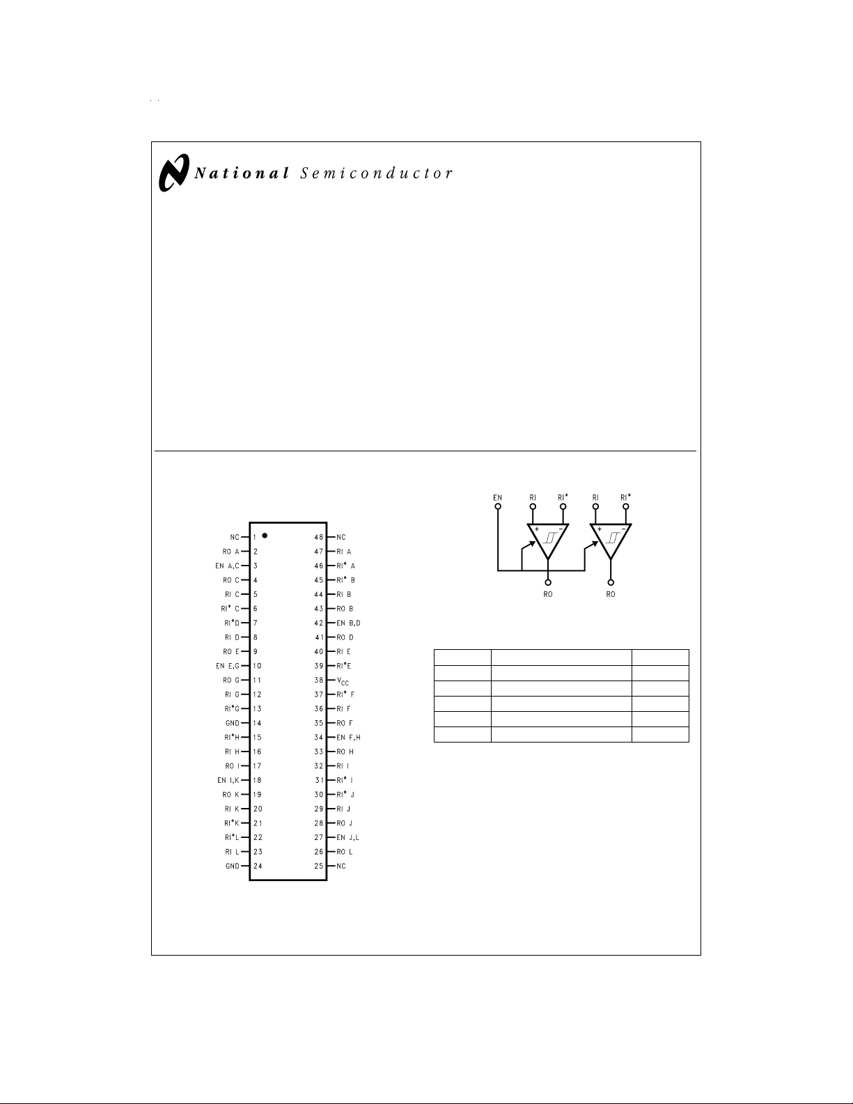
Each TRI-STATE
be active or in a Hi-impedance off state. Each enable is common to only two receivers for flexibility and multiplexingofreceiver outputs.
The receiver output (RO)is guaranteed to be Highwhen the
inputs are left open and unterminated. The receiver can detect signals as low and including
mode range of
ible with both TTL and CMOS levels.
®
enable, EN, allows the receiver output to
±
±
7V.The receiver outputs (RO) are compat-
200 mV over the common
Features
n Low power design—240 mW typical
n Meets TIA/EIA-422-B (RS-422)
n Receiver OPEN input failsafe feature
n Guaranteed AC parameters:
— Maximum receiver skew −4 ns
— Maximum transition time −9 ns
n High Output Drive Capability:
n Available in SSOP packaging:
— Requires 30%less PCB space than 3 DS34C86TMs
Connection Diagram Function Diagram
48L SSOP
DS89C386
1/6 of package
Truth Table
Enable Inputs Output
EN RI–RI
LXZ
H≥200 mV or OPEN
H ≤ −200 mV L
H +200 mV
†
Not terminated.
>
±
6mA
DS012085-2
*
†
and>−200 mV X
RO
H
DS012085-1
Order Number DS89C386TMEA
See NS Package Number MS48A
TRI-STATE®is a registered trademarkof National Semiconductor Corporation.
© 1998 National Semiconductor Corporation DS012085 www.national.com
Absolute Maximum Ratings (Notes 1, 2)
If Military/Aerospace specified devices are required,
please contact the National Semiconductor Sales Office/
SSOP Package 1359 mW
±
Current Per Output
25 mA
This device does not meet 2000V ESD rating. (Note 5)
Distributors for availability and specifications.
Supply Voltage (V
Input Common Mode Range (V
Differential Input Voltage (V
Enable Input Voltage (V
Storage Temperature Range (T
) −0.5 to 7V
CC
IN)
)
CM
)
DIFF
) −65˚C to +150˚C
STG
±
14V
±
14V
Lead Temperature (Soldering 4 sec) 260˚C
Operating Conditions
Supply Voltage (V
7V
Operating Temperature Range (T
DS89C386T −40 +85 ˚C
Enable Input Rise or Fall Times 500 ns
) 4.50 5.50 V
CC
)
A
Min Max Unit
Maximum Power Dissipation at 25˚C (Note 4)
DC Electrical Characteristics (Note 3)
=
V
Symbol Parameter Conditions Min Typ Max Units
V
TH
V
HYST
R
IN
I
IN
V
OH
V
OL
V
IH
V
IL
I
OZ
I
I
I
CC
±
10%(unless otherwise specified)
5V
CC
Differential Input Voltage V
Input Hysteresis V
Input Resistance V
=
or V
V
OUT
OH
<
−7V
V
=
0V 70 mV
CM
=
−7V, +7V 5.0 6.8 10 kΩ
IN
OL
<
+7V
CM
−200
±
35 +200 mV
(Other Input=GND)
Input Current V
(Under Test) V
High Level Output Voltage V
Low Level Output Voltage V
Enable High Input Level Voltage 2.0 V
=
+10V, Other Input=GND +1.1 +1.5 mA
IN
=
−10V, Other Input=GND −2.0 −2.5 mA
IN
=
Min., V
CC
=
I
−6.0 mA
OUT
=
Max., V
CC
=
I
6.0 mA
OUT
=
+1V 3.8 4.2 V
(DIFF)
=
−1V 0.2 0.3 V
(DIFF)
CC
V
Enable Low Input Level Voltage GND 0.8 V
TRI-STATE Output Leakage Current V
Enable Input Current V
Quiescent Power Supply Current V
OUT
IN
CC
=
=
V
=
V
CC
Max., V
or GND, EN=V
CC
or GND
=
(DIFF)
IL
+1V 48 69 mA
±
0.5
±
5.0 µA
±
1.0 µA
www.national.com 2
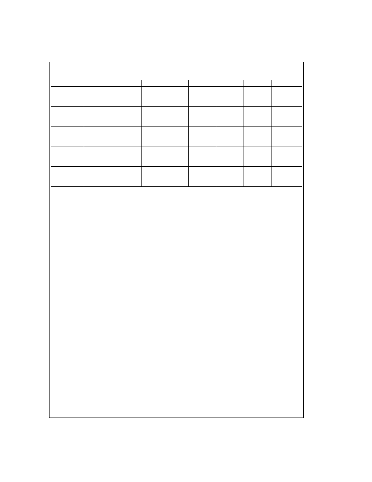
AC Electrical Characteristics (Note 3)
=
V
t
PLH
t
PHL
t
SK
t
RISE
t
FALL
t
PLZ
t
PHZ
t
PZL
t
PZH
Note 1: Absolute Maximum Ratings are those values beyond which the safety of the device cannot be guaranteed. They are not meant to imply that the device
should be operated at these limits. The table of “Electrical Characteristics” provides conditions for actual device operation.
Note 2: Unless otherwise specified, all voltages are referenced to ground.
Note 3: Unless otherwise specified, Min/Max limits apply across the operating temperature range.All typicals are given for V
Note 4: Ratings apply to ambient temperature at 25˚C. Above this temperature derate SSOP (MEA) Package 10.9 mW/˚C.
Note 5: ESD Rating: HEM (1.5 kΩ, 100 pF)
±
10%(
5V
CC
Figures 1, 2, 3
)
Symbol Parameter Conditions Min Typ Max Units
, Propagation Delay C
Input to Output V
Skew C
, Output Rise and C
Fall Times V
, Propagation Delay C
ENABLE to Output R
, Propagation Delay C
ENABLE to Output R
Inputs ≥ 2000V
Outputs ≥ 1000V
EIAJ (0Ω, 200 pF)
All Pins ≥ 350V
=
50 pF
L
=
2.5V 10 19 30 ns
DIFF
=
V
0V
CM
=
50 pF
L
=
V
2.5V 0 2 4 ns
DIFF
=
V
0V
CM
=
50 pF
L
=
2.5V 4 9 ns
DIFF
=
V
0V
CM
=
50 pF
L
=
1000Ω 13 18 ns
L
=
V
2.5V
DIFF
=
50 pF
L
=
1000Ω 13 21 ns
L
=
V
2.5V
DIFF
=
5V and T
CC
=
25˚C.
A
www.national.com3
 Loading...