NSC DS7837J-883 Datasheet

TL/F/5811
DS7837/DS8837 Hex Unified Bus Receiver
February 1996
DS7837/DS8837 Hex Unified Bus Receiver
General Description
The DS7837/DS8837 are high speed receivers designed for
use in bus organized data transmission systems interconnected by terminated 120X impedance lines. The external
termination is intended to be 180X resistor from the bus to
the
a
5V logic supply together with a 390X resistor from the
bus to ground. The receiver design employs a built-in input
hysteresis providing substantial noise immunity. Low input
current allows up to 27 driver/receiver pairs to utilize a common bus. Disable inputs provide time discrimination. Disable
inputs and receiver outputs are TTL compatible. Performance is optimized for systems with bus rise and fall times
s
1.0 ms/V.
Features
Y
Low receiver input current for normal VCCor V
CC
e
0V
(15 mA typ)
Y
Six separate receivers per package
Y
Built-in receiver input hysteresis (1V typ)
Y
High receiver noise immunity (2V typ)
Y
Temperature insensitive receiver input thresholds track
bus logic levels
Y
TTL compatible disable and output
Y
Molded or cavity dual-in-line or flat package
Y
High speed
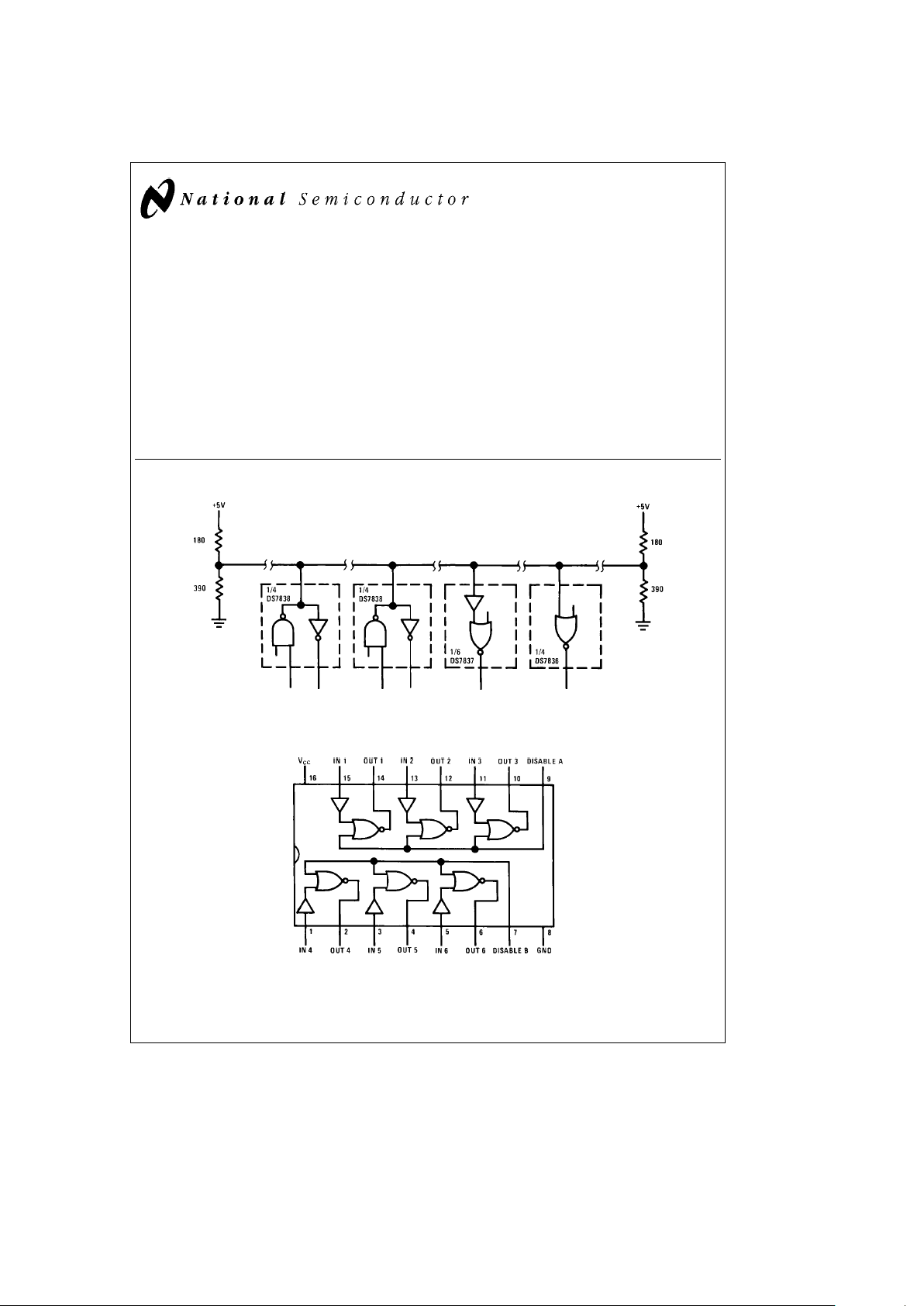
Typical Application
TL/F/5811– 1
Connection Diagram
Dual-In-Line Package
TL/F/5811– 2
Top View
Order Number DS7837J, DS8837M or DS8837N
See NS Package Number J16A, M16A or N16A
C
1996 National Semiconductor Corporation RRD-B30M36/Printed in U. S. A.
http://www.national.com

Absolute Maximum Ratings (Note 1)
If Military/Aerospace specified devices are required,
please contact the National Semiconductor Sales
Office/Distributors for availability and specifications.
Supply Voltage 7V
Input Voltage 5.5V
Operating Temperature Range
DS7837
b
55§Ctoa125§C
DS8837 0
§
Ctoa70§C
Storage Temperature Range
b
65§Ctoa150§C
Maximum Power Dissipation* at 25
§
C
Cavity Package 1433 mW
Molded DIP Package 1362 mW
SO Package 1002 mW
Lead Temperature (Soldering, 4 seconds) 260
§
C
*Derate cavity package 9.6 mW/§C above 25§C; derate molded DIP package
10.9 mW/
§
C above 25§C; derate SO package 8.01 mW/§C above 25§C.
Operating Conditions
Min Max Units
Supply Voltage, (V
CC
)
DS7837 4.5 5.5 V
DS8837 4.75 5.25 V
Temperature (T
A
)
DS7837
b
55
a
125
§
C
DS8837 0
a
70
§
C
Electrical Characteristics
The following apply for V
MIN
s
V
CC
s
V
MAX,TMIN
s
T
A
s
T
MAX
, unless otherwise specified (Notes 2 and 3)
Symbol Parameter Conditions Min Typ Max Units
V
TH
High Level Receiver Threshold V
CC
e
Max DS7837 1.65 2.25 2.65 V
DS8837 1.80 2.25 2.50 V
V
TL
Low Level Receiver Threshold V
CC
e
Min DS7837 0.97 1.30 1.63 V
DS8837 1.05 1.30 1.55 V
I
IH
Maximum Receiver Input Current V
IN
e
4V V
CC
e
V
MAX
15.0 50.0 mA
V
CC
e
0V 1.0 50.0 mA
I
IL
Logical ‘‘0’’ Receiver Input Current V
IN
e
0.4V, V
CC
e
V
MAX
1.0 50.0 mA
V
IH
Logical ‘‘1’’ Input Voltage Disable 2.0 V
V
IL
Logical ‘‘0’’ Input Voltage Disable 0.8 V
I
IH
Logical ‘‘1’’ Input Current Disable Input V
IND
e
2.4V 80.0 mA
V
IND
e
5.5V 2.0 mA
I
IL
Logical ‘‘0’’ Input Current V
IN
e
4V, V
IND
e
0.4V, Disable Input
b
3.2 mA
V
OH
Logical ‘‘1’’ Output Voltage V
IN
e
0.5V, V
IND
e
0.8V,
2.4 V
I
OH
eb
400 mA
V
OL
Logical ‘‘0’’ Output Voltage V
IN
e
4V, V
IND
e
0.8V, I
OH
e
16 mA 0.25 0.4 V
I
OS
Output Short Circuit Current V
IN
e
0.5V, V
IND
e
0V, V
OS
e
0V,
b
18.0
b
55.0 mA
V
CC
e
V
MAX
, (Note 4)
I
CC
Power Supply Current V
IN
e
4V, V
IND
e
0V, (Per Package) 45.0 60.0 mA
V
CL
Input Clamp Diode V
IN
eb
12 mA, V
IND
eb
12 mA,
b
1.0
b
1.5 V
T
A
e
25§C
http://www.national.com 2
 Loading...