

NSC DS15BA101SD, DS15BA101 Datasheet

April 2007
DS15BA101
1.5 Gbps Differential Buffer with Adjustable Output Voltage
General Description
The DS15BA101 is a high-speed differential buffer for cable
driving, level translation, signal buffering, and signal repeating applications. Its fully differential signal path ensures exceptional signal integrity and noise immunity and it drives both
differential and single-ended transmission lines at data rates
in excess of 1.5 Gbps.
Output voltage amplitude is adjustable via a single external
resistor for level translation and cable driving applications into
50-ohm single-ended and 100-ohm differential mode
impedances.
The DS15BA101 is powered from a single 3.3V supply and
consumes 150 mW (typ) at 1.5 Gbps. It operates over the full
−40°C to +85°C industrial temperature range and is available
in a space saving 3x3 mm LLP-8 package.
Features
■
Data rates from DC to 1.5+ Gbps
■
Differential or single-ended input
■
Adjustable output amplitude
■
Single 3.3V supply
■
Industrial -40°C to +85°C temperature
■
Low power: 150 mW (typ) at 1.5 Gbps
■
Space-saving 3 x 3 mm LLP-8 package
Applications
■
Cable extension applications
■
Level translation
■
Signal buffering and repeating
■
Security cameras
Typical Application
20199902
© 2007 National Semiconductor Corporation 201999 www.national.com
DS15BA101 1.5 Gbps Differential Buffer with Adjustable Output Voltage

Absolute Maximum Ratings (Note 1)
Supply Voltage: −0.5V to 3.6V
Input Voltage (all inputs) −0.3V to VCC+0.3V
Output Current 28 mA
Storage Temperature Range −65°C to +150°C
Junction Temperature +150°C
Lead Temperature
(Soldering 4 Sec) +260°C
Package Thermal Resistance
θJA LLP-8
θJC LLP-8
+90.7°C/W
+41.2°C/W
ESD Rating (HBM) 5 kV
ESD Rating (MM) 250V
Recommended Operating
Conditions
Supply Voltage (VCC – GND): 3.3V ±5%
Operating Free Air Temperature (TA)
DS15BA101SD −40°C to +85°C
DC Electrical Characteristics
Over Supply Voltage and Operating Temperature ranges, unless otherwise specified (Notes 2, 3).
Symbol Parameter Conditions Reference Min Typ Max Units
V
ICM
Input Common Mode Voltage (Note 4) IN+, IN-
0.8
VCC –
VID/2
V
V
ID
Differential Input Voltage Swing
100 2000
mV
P−P
V
OS
Output Common Mode Voltage OUT+, OUT-
VCC –
V
OUT
/2
V
V
OUT
Output Voltage
Single-ended, 50Ω load
RVO = 953Ω 1%,
400
mV
P-P
Single-ended, 50Ω load
RVO = 487Ω 1%,
800
mV
P-P
I
CC
Supply Current (Note 5)
45 49 mA
AC Electrical Characteristics
Over Supply Voltage and Operating Temperature ranges, unless otherwise specified (Note 3).
Symbol Parameter Conditions Reference Min Typ Max Units
DR
MAX
Maximum Data Rate (Note 4) IN+, IN-
1.5 2.0 Gbps
t
LHT
Output Low to High Transition
Time
20% – 80%
(Note 6)
OUT+, OUT-
120 220 ps
t
HLT
Output High to Low Transition
Time
120 220 ps
t
PLHD
Propagation Low to High Delay (Note 4)
0.95 1.10 1.35 ns
t
PHLD
Propagation High to Low Delay (Note 4)
0.95 1.10 1.35 ns
t
TJ
Total Jitter 1.5 Gbps
26
ps
P-P
Note 1: "Absolute Maximum Ratings" are those parameter values beyond which the life and operation of the device cannot be guaranteed. The stating herein of
these maximums shall not be construed to imply that the device can or should be operated at or beyond these values. The table of "Electrical Characteristics"
specifies acceptable device operating conditions.
Note 2: Current flow into device pins is defined as positive. Current flow out of device pins is defined as negative. All voltages are stated referenced to GND.
Note 3: Typical values are stated for VCC = +3.3V and TA = +25°C.
Note 4: Specification is guaranteed by characterization.
Note 5: Maximum ICC is measured at VCC = +3.465V and TA = +70°C.
Note 6: Specification is guaranteed by characterization and verified by test.
www.national.com 2
DS15BA101
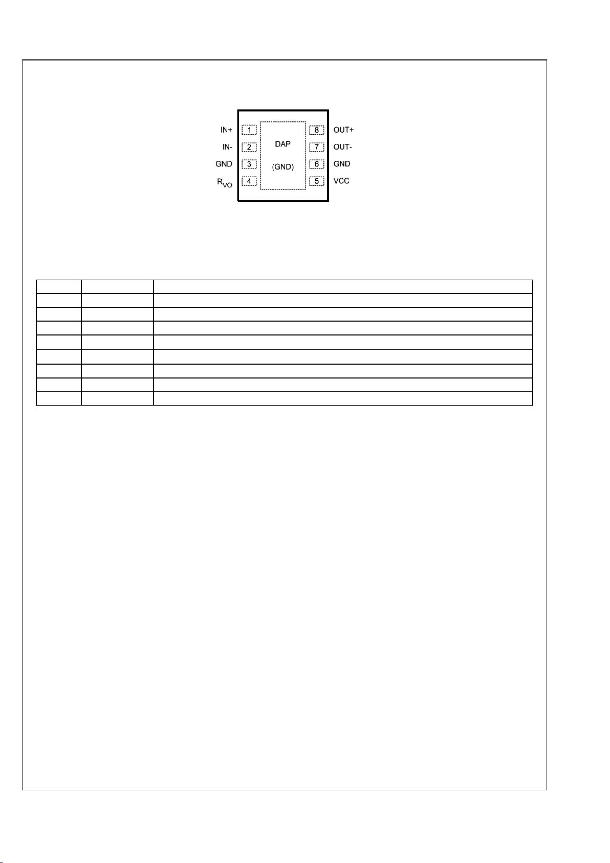
Connection Diagram
20199901
8-Pad LLP
Order Number DS15BA101SD or DS15BA101SDX
See NS Package Number SDA08A
Pin Descriptions
Pin # Name Description
1 IN+ Non-inverting input pin.
2 IN- Inverting input pin.
3 GND Circuit common (ground reference).
4 R
VO
Output voltage amplitude control. Connect a resistor to VCC to set output voltage.
5 V
CC
Positive power supply (+3.3V).
6 GND Circuit common (ground reference).
7 OUT- Non-inverting output pin.
8 OUT+ Inverting output pin.
3 www.national.com
DS15BA101
 Loading...