

NSC DS14C88N, DS14C88MX, DS14C88M Datasheet
DS14C88
QUAD CMOS Line Driver
General Description
The DS14C88, pin-for-pin compatible to the DS1488/
MC1488, is a quad line drivers designed to interface data
terminal equipment (DTE) with data circuit-terminating
equipment (DCE). This device translates standard TTL/
CMOS logic levels to levels conforming to EIA-232-D and
CCITT V.28 standards.
The device is fabricated in low threshold CMOS metal gate
technology. The device provides very low power consumption compared to its bipolar equivalents: 500 µA (DS14C88)
versus 25 mA (DS1488).
The DS14C88 simplifies designs byeliminating the need for
external slew rate control capacitors. Slew rate control in accordance with EIA-232D is provided on-chip, eliminating the
output capacitors.
Features
n Meets EIA-232D and CCITT V.28 standards
n LOW power consumption
n Wide power supply range:
±
5V to±12V
n Available in SOIC package
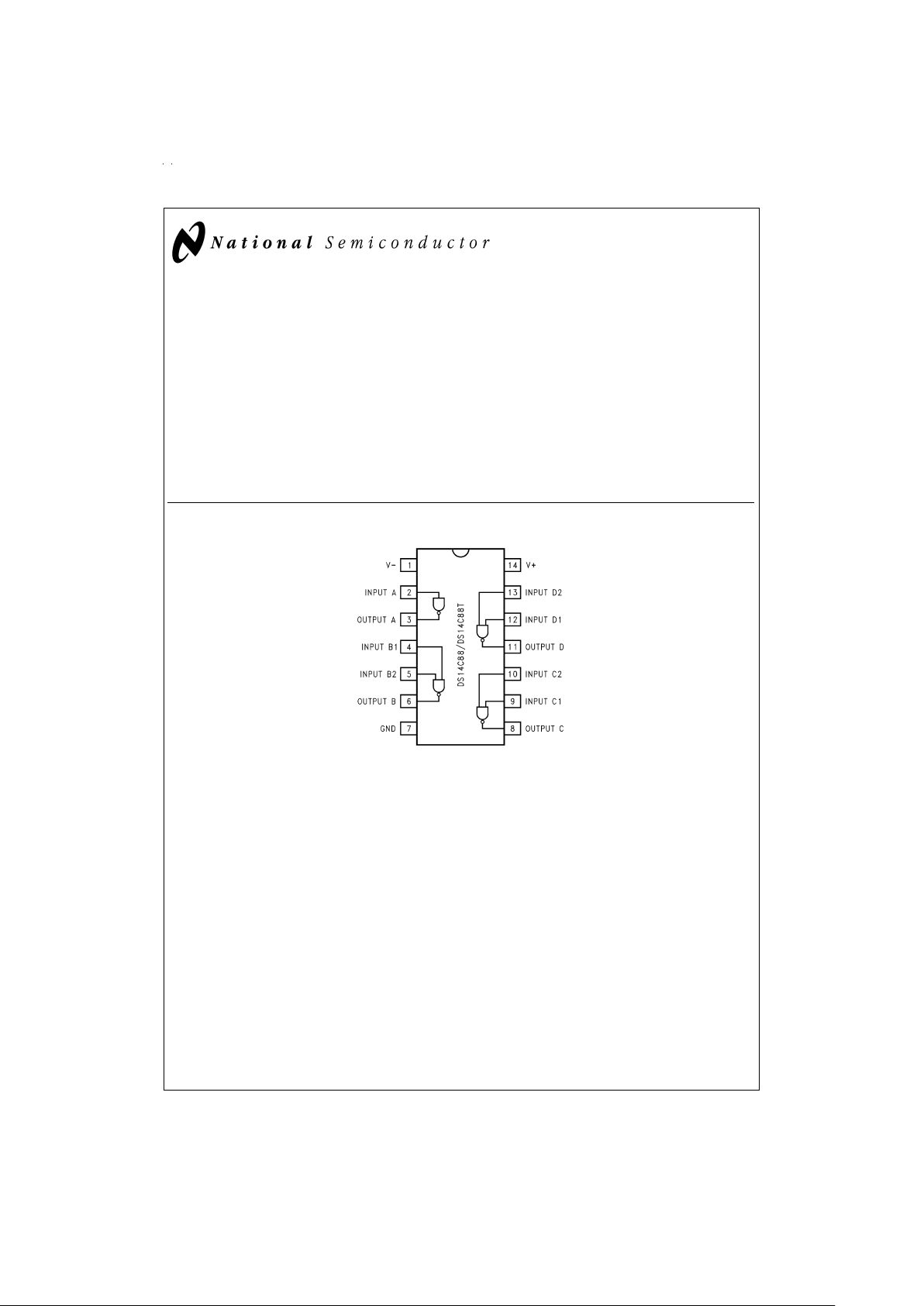
Connection Diagram
DS011105-1
Order Number DS14C88N, or DS14C88M
See NS Package Number N14A or M14A
May 1998
DS14C88 QUAD CMOS Line Driver
© 1998 National Semiconductor Corporation DS011105 www.national.com
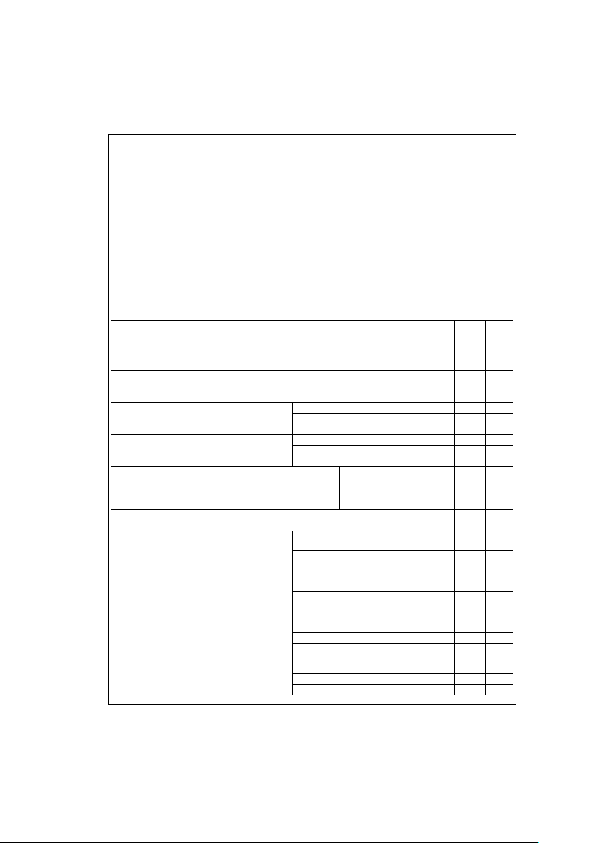
Absolute Maximum Ratings (Note 1)
If Military/Aerospace specified devices are required,
please contact the National Semiconductor Sales Office/
Distributors for availability and specifications.
Supply Voltage
V
+
Pin +13V
V
−
Pin −13V
Driver Input Voltage (V
+
) +0.3V to GND
−0.3V
Driver Output Voltage |(V
+
)−VO|≤30V
|(V
−
)−VO|≤30V
Continuous Power Dissipation
@
+25˚C (Note 2)
N Package 1513 mW
M Package 1063 mW
Junction Temperature +150˚C
Lead Temperature
(Soldering 4 seconds) +260˚C
Storage Temperature Range −65˚C to +150˚C
This Product does not meet 2000V ESD rating. (Note 9)
Recommended Operating
Conditions
Min Max Units
V
+
Supply (GND=0V) +4.5 +12.6 V
V
−
Supply (GND=0V) −4.5 −12.6 V
Operating Free Air Temp.
(T
A
)
DS14C88 0 +75 ˚C
Electrical Characteristics
Over Recommended Operating Conditions, unless otherwise specified
Symbol Parameter Conditions Min Typ Max Units
I
IL
Maximum Low Input
Current
V
IN
=
GND +10 µA
I
IH
Maximum High Input
Current
V
IN
=
V
+
−10 µA
V
IL
Low Level Input Voltage V+≥ +7V, V−≤ −7V GND 0.8 V
V
+
<
+7V, V
−
>
−7V GND 0.6 V
V
IH
High Level Input Voltage 2.0 V
+
V
V
OL
Low Level Output Level V
IN
=
V
IH
V
+
=
4.5V, V
−
=
−4.5V −4.0 −3.0 V
R
L
=
3kΩ V
+
=
9V, V
−
=
9V −8.0 −6.5 V
or7kΩ V
+
=
12V, V
−
=
−12V −10.5 −9.0 V
V
OH
High Level Output Level V
IN
=
V
IL
V
+
=
4.5V, V
−
=
−4.5V 3.0 4.0 V
R
L
=
3kΩ V
+
=
9V, V
−
=
−9V 6.5 8.0 V
or7kΩ V
+
=
12V, V
−
=
−12V 9.0 10.5 V
I
OS+
High Level Output Short V
IN
=
0.8V, V
O
=
GND V
+
=
+12V, −45 mA
Circuit Current (Note 3) V
−
=
−12V
I
OS−
Low Level Output Short V
IN
=
2.0V, V
O
=
GND +45 mA
Circuit Current (Note 3)
R
OUT
Output Resistance V
+
=
V
−
=
GND=0V 300 Ω
−2V ≤ V
O
≤ +2V (Note 4) (
Figure 1
)
I
CC+
Positive Supply Current V
IN
=
V
ILmax
V
+
=
4.5V, V
−
=
−4.5V 10 µA
R
L
=
OPEN V
+
=
9V, V
−
=
−9V 30 µA
V
+
=
12V, V
−
=
−12V 60 µA
V
IN
=
V
IHmin
V
+
=
4.5V, V
−
=
−4.5V 50 µA
R
L
=
OPEN V
+
=
9V, V
−
=
−9V 300 µA
V
+
=
12V, V
−
=
−12V 500 µA
I
CC-
Negative Supply Current V
IN
=
V
ILmax
V
+
=
4.5V, V
−
=
−4.5V −10 µA
R
L
=
OPEN V
+
=
9V, V
−
=
−9V −10 µA
V
+
=
12V, V
−
=
−12V −10 µA
V
IN
=
V
IHmin
V
+
=
4.5V, V
−
=
−4.5V −30 µA
R
L
=
OPEN V
+
=
9V, V
−
=
−9V −30 µA
V
+
=
12V, V
−
=
−12V −60 µA
www.national.com 2
 Loading...