

DS14C335
+3.3V Supply TIA/EIA-2323x5Driver/Receiver
General Description
The DS14C335 is three driver, five receiver device which
conforms to TIA/EIA-232-E and CCITT V.28 standard specifications. This device employs an internal DC-DC converter
to generate the necessary output levels from a +3.3V power
supply. A SHUTDOWN (SD) mode reduces the supply current to 10 µAmaximum. In the SD mode, one receiver is active, allowing ring indicator (RI) to be monitored. PC Board
space consumption is minimized by the availability of Shrink
Small Outline Packaging (SSOP).
This device’s low power requirement and small footprint
makes it an ideal choice for Laptop and Notebook applications.
Features
n Conforms to TIA/EIA-232-E and CCITT V.28
specifications
n Operates with single +3.3V power supply
n Low power requirement—I
CC
20 mA maximum
n SHUTDOWN mode—I
CX
10 µA maximum
n One Receiver (R5) active during SHUTDOWN
n Operates up to 128 kbps —Lap-Link
®
Compatible
n Flow through pinout
n 4V/µs minimum Slew Rate guaranteed
n Inter-operates with +5V UARTs
n Available in 28-lead SSOP EIAJ Type II package
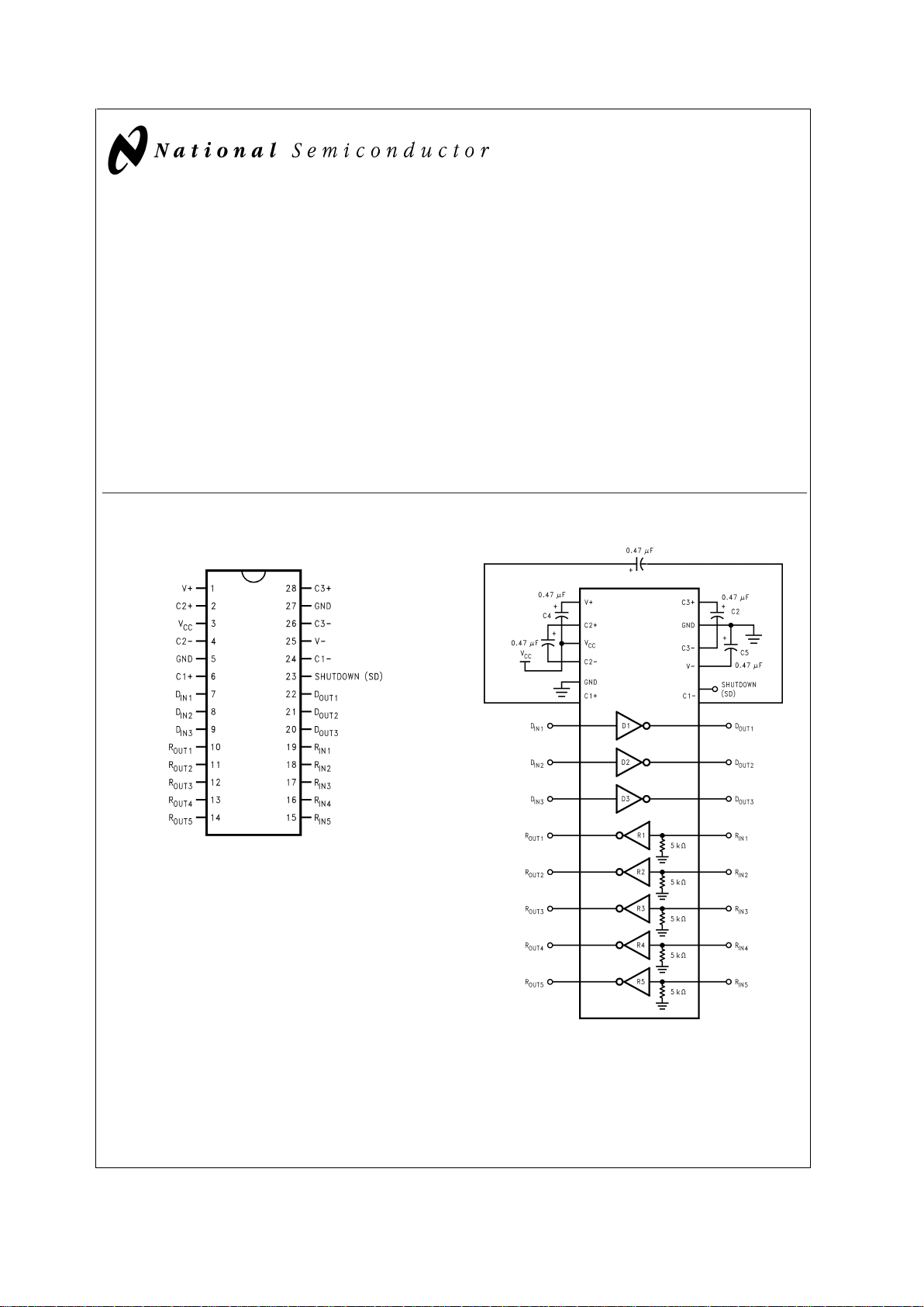
Connection Diagram Functional Diagram
Lap-Link®is a registered trademark of Traveling Software.
DS14C335
DS011734-1
Order Number DS14C335MSA
See NS Package Number MSA28
DS011734-2
March 2000
DS14C335 +3.3V Supply TIA/EIA-2323x5Driver/Receiver
© 2000 National Semiconductor Corporation DS011734 www.national.com
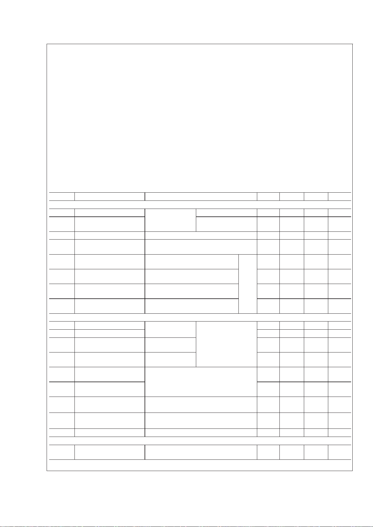
Absolute Maximum Ratings (Note 1)
If Military/Aerospace specified devices are required,
please contact the National Semiconductor Sales Office/
Distributors for availability and specifications.
Supply Voltage (V
CC
) −0.3V to + 6V
V
+
Pin (VCC−0.3V) to +14V
V
−
Pin +0.3V to −14V
Input Voltage (DIN, SD) −0.3V to + 5.5V
Driver Output Voltage (V
+
+ 0.3V) to (V−−0.3V)
Receiver Input Voltage
±
25V
Receiver Output Voltage −0.3V to (V
CC
+ 0.3V)
Junction Temperature +150˚C
Storage Temperature Range −65˚C to +150˚C
Lead Temperature
(Soldering 4 sec.) +260˚C
Short Circuit Duration (D
OUT
) continuous
Maximum Package Power Dissipation
@
+25˚C
SSOP MSA Package 1286 mW
Derate MSA Package 10.3 mW/˚C above +25˚C
ESD Rating
(HBM, 1.5 kΩ, 100 pF) ≥ 2.0 kV
Recommended Operating
Conditions
Min Max Units
Supply Voltage (V
CC
) 3.0 3.6 V
DC-DC Converter Capacitors
(C1–C5)
0.47 µF
Operating Free Air Temperature (T
A
)
DS14C335 0 +70 ˚C
Electrical Characteristics (Notes 2, 3)
Over recommended operating conditions, SD = 0.8V, unless otherwise specified.
Symbol Parameter Conditions Min Typ Max Units
DEVICE CHARACTERISTICS
V+ Positive Power Supply No Load D
IN
= 0.8V +9.3 V
V− Negative Power Supply C1–C5 = 0.47
µF
D
IN
= 2.0V −9.0 V
I
CC
Supply Current No Load 11.5 20 mA
I
CX
SHUTDOWN Supply
Current
RL=3kΩ,SD=VCC, 5.5V 1.0 10 µA
V
IH
High Level Enable
Voltage
SD 2.0 V
V
IL
Low Level Enable
Voltage
GND 0.8 V
I
IH
High Level Enable
Current
2.0V ≤ VIN≤ 5.5V +2.0 µA
I
IL
Low Level Enable
Current
GND ≤ VIN≤ 0.8V −2.0 µA
DRIVER CHARACTERISTICS
V
IH
High Level Input Voltage D
IN
2.0 V
V
IL
Low Level Input Voltage GND 0.8 V
I
IH
High Level Input Current 2.0V ≤ VIN≤
5.5V
+1.0 µA
I
IL
Low Level Input Current GND ≤ VIN≤
0.8V
−1.0 µA
V
OH
High Level Output
Voltage
RL=3kΩ +5.0 +7.1 V
V
OL
Low Level Output
Voltage
−6.3 −5.0 V
I
OS+
Output High Short VO= 0V, VIN= 0.8V (Note 7) −40 −16.5 −8 mA
Circuit Current
I
OS−
Output Low Short VO= 0V, VIN= 2.0V (Note 7) 6 12.3 40 mA
Circuit Current
R
O
Output Resistance −2V ≤ VO≤ +2V, VCC= GND = 0V 300 Ω
RECEIVER CHARACTERISTICS (Note 4)
V
TH
Input High Threshold
Voltage
R1–R5, SD = 0.8V 1.4 2.4 V
DS14C335
www.national.com 2
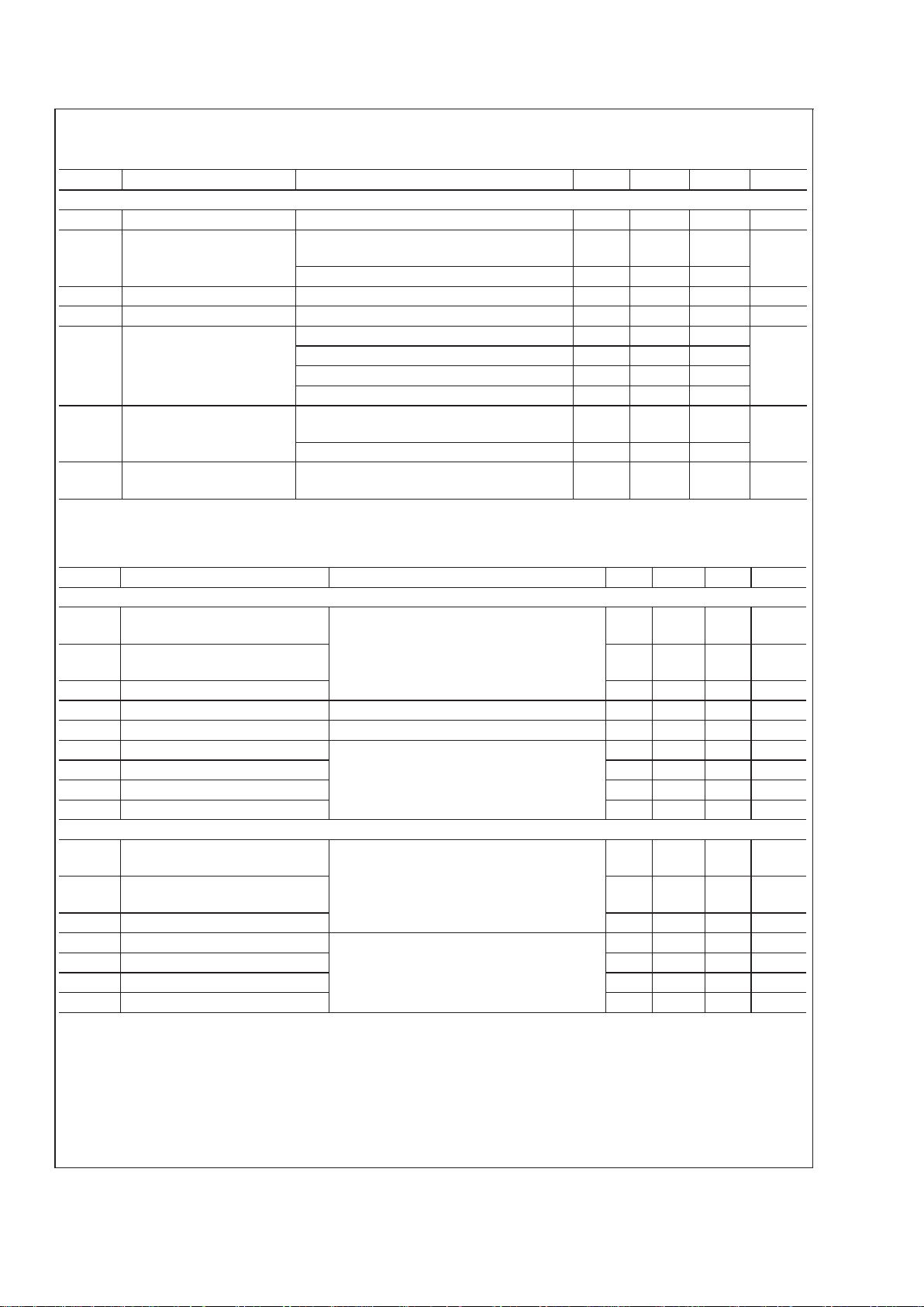
Electrical Characteristics (Notes 2, 3) (Continued)
Over recommended operating conditions, SD = 0.8V, unless otherwise specified.
Symbol Parameter Conditions Min Typ Max Units
RECEIVER CHARACTERISTICS (Note 4)
R5, 2.0V ≤ SD ≤ 5.5V 2.0 2.8 V
V
TL
Input Low Threshold
Voltage
R1–R5, SD = 0.8V 0.4 1.1 V
R5, 2.0V ≤ SD ≤ 5.5V 0.1 0.5 V
V
HY
Hysteresis 50 300 mV
R
IN
Input Resistance VIN=±3V to±15V 3.0 3.8 7.0 kΩ
I
IN
Input Current VIN= +15V 2.14 5.0 mA
V
IN
= +3V 0.43 1.0 mA
V
IN
= −3V −1.0 −0.43 mA
V
IN
= −15V −5.0 −2.14 mA
V
OH
High Level Output
Voltage
VIN= −3V, IOH= −1 mA 2.4 3.1 V
V
IN
= −3V, IOH= −100 µA 2.8 3.28 V
V
OL
Low Level Output
Voltage
VIN= +3V, IOL= +2 mA 0.23 0.4 V
Switching Characteristics (Note 2)
Over recommended operating conditions, SD = 0.8V, unless otherwise specified.
Symbol Parameter Conditions Min Typ Max Units
DRIVER CHARACTERISTICS
t
PLH
Propagation Delay LOW to
HIGH
RL=3kΩ
C
L
=50pF
(
Figures 1, 2
)
0.1 0.6 1.0 µs
t
PHL
Propagation Delay HIGH to
LOW
0.1 0.6 1.0 µs
t
SK
Skew |t
PLH–tPHL
| 0 0.2 µs
SR1 Output Slew Rate R
L
=3kΩto7kΩ,CL=50pF(
Figure 2
) 4 13 30 V/µs
SR2 Output Slew Rate R
L
=3kΩ,CL= 2500 pF (
Figure 2
) 4 10 30 V/µs
t
PLS
Propagation Delay LOW to SD (
Figures 5, 6
)
R
L
=3kΩ
C
L
=50pF
0.48 ms
t
PSL
Propagation Delay SD to LOW 1.88 ms
t
PHS
Propagation Delay HIGH to SD 0.62 ms
t
PSH
Propagation Delay SD to HIGH 1.03 ms
RECEIVER CHARACTERISTICS
t
PLH
Propagation Delay LOW to
HIGH
CL=50pF
(
Figures 3, 3
)
0.1 0.4 1.0 µs
t
PHL
Propagation Delay HIGH to
LOW
0.1 0.6 1.0 µs
t
SK
Skew |t
PLH–tPHL
| 0.2 0.8 µs
t
PLS
Propagation Delay LOW to SD (
Figures 7, 8
)
R
L
=1kΩ
C
L
=50pF
R1–R4 Only
0.13 µs
t
PSL
Propagation Delay SD to LOW 1.0 µs
t
PHS
Propagation Delay HIGH to SD 0.19 µs
t
PSH
Propagation Delay SD to HIGH 0.58 µs
Note 1: “Absolute Maximum Ratings” are those values beyond which the safety of the device cannot be guaranteed. They are not meant to imply that the devices
should be operated at these limits. The tables of “Electrical Characteristics” specify conditions for device operation.
Note 2: Typical values are given for V
CC
= 3.3V and TA= +25˚C.
Note 3: Current into device pins is defined as positive. Current out of device pins is defined as negative. All voltages are referenced to ground unless otherwise specified.
Note 4: Receiver characteristics are guaranteed for SD = 0.8V. When SD = 2.0V,receiver five (R5) is active and meets receiver parameters in SHUTDOWN (SD)
mode, unless otherwise specified.
Note 5: Generator characteristics for driver input: f = 64 kHz (128 kbits/sec), t
r=tf
<
10 ns, VIH=3V,VIL= 0V, duty cycle = 50%.
Note 6: Generator characteristics for receiver input: f = 64 kHz (128 kbits/sec), t
r=tf
= 200 ns, VIH=3V,VIL= −3V, duty cycle = 50%.
DS14C335
www.national.com3
 Loading...