

DS14C335
+3.3V Supply TIA/EIA-2323x5Driver/Receiver
General Description
The DS14C335 is three driver, five receiver device which
conforms to TIA/EIA-232-E and CCITT V.28 standard specifications. This device employs an internal DC-DC converter
to generate the necessary output levels from a +3.3V power
supply. A SHUTDOWN (SD) mode reduces the supply current to 10 µAmaximum. In the SD mode, one receiver is active, allowing ring indicator (RI) to be monitored. PC Board
space consumption is minimized by the availability of Shrink
Small Outline Packaging (SSOP).
This device’s low power requirement and small footprint
makes it an ideal choice for Laptop and Notebook applications.
Features
n Conforms to TIA/EIA-232-E and CCITT V.28
specifications
n Operates with single +3.3V power supply
n Low power requirement—I
CC
20 mA maximum
n SHUTDOWN mode—I
CX
10 µA maximum
n One Receiver (R5) active during SHUTDOWN
n Operates up to 128 kbps —Lap-Link
®
Compatible
n Flow through pinout
n 4V/µs minimum Slew Rate guaranteed
n Inter-operates with +5V UARTs
n Available in 28-lead SSOP EIAJ Type II package
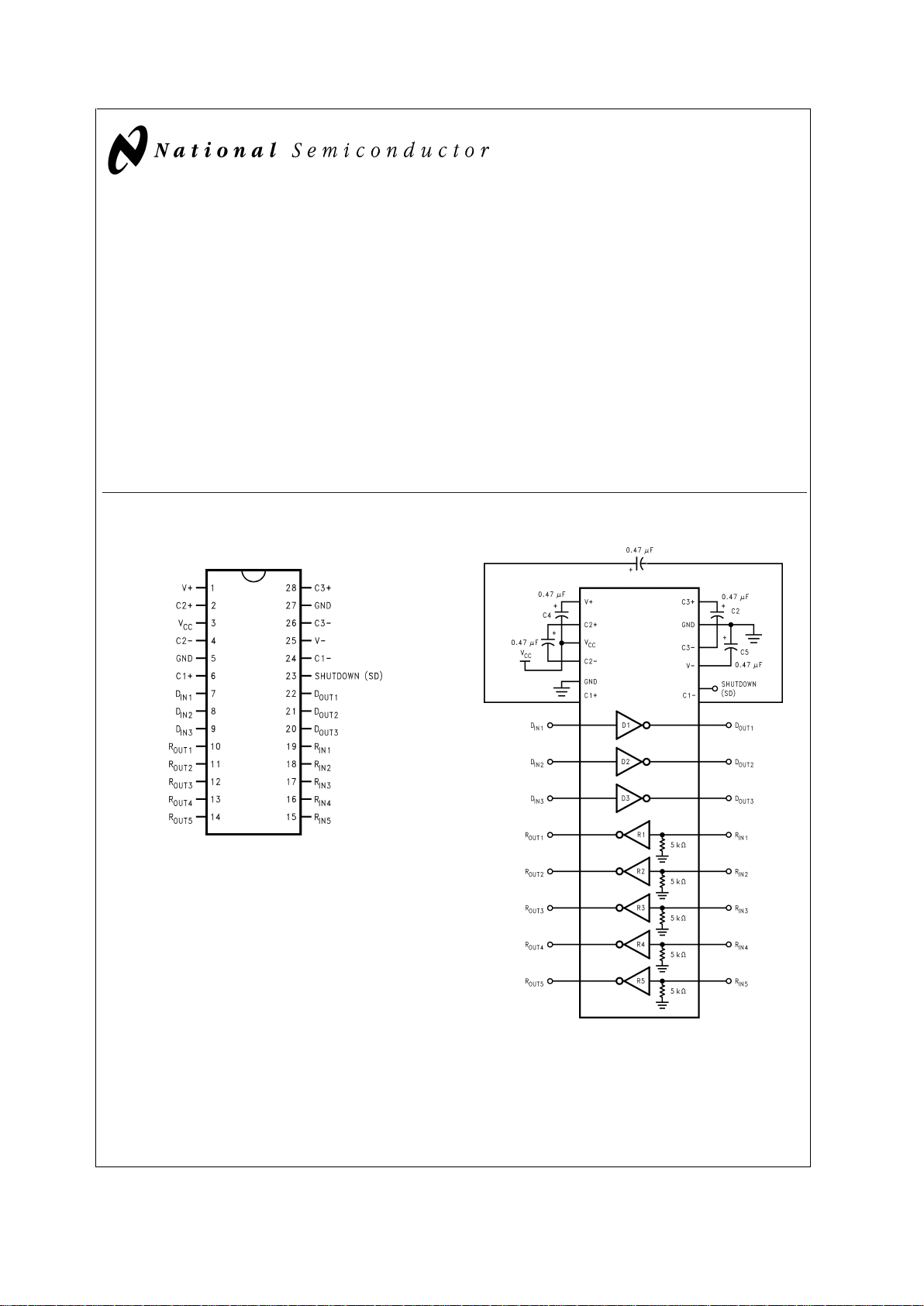
Connection Diagram Functional Diagram
Lap-Link®is a registered trademark of Traveling Software.
DS14C335
DS011734-1
Order Number DS14C335MSA
See NS Package Number MSA28
DS011734-2
March 2000
DS14C335 +3.3V Supply TIA/EIA-2323x5Driver/Receiver
© 2000 National Semiconductor Corporation DS011734 www.national.com
Absolute Maximum Ratings (Note 1)
If Military/Aerospace specified devices are required,
please contact the National Semiconductor Sales Office/
Distributors for availability and specifications.
Supply Voltage (V
CC
) −0.3V to + 6V
V
+
Pin (VCC−0.3V) to +14V
V
−
Pin +0.3V to −14V
Input Voltage (DIN, SD) −0.3V to + 5.5V
Driver Output Voltage (V
+
+ 0.3V) to (V−−0.3V)
Receiver Input Voltage
±
25V
Receiver Output Voltage −0.3V to (V
CC
+ 0.3V)
Junction Temperature +150˚C
Storage Temperature Range −65˚C to +150˚C
Lead Temperature
(Soldering 4 sec.) +260˚C
Short Circuit Duration (D
OUT
) continuous
Maximum Package Power Dissipation
@
+25˚C
SSOP MSA Package 1286 mW
Derate MSA Package 10.3 mW/˚C above +25˚C
ESD Rating
(HBM, 1.5 kΩ, 100 pF) ≥ 2.0 kV
Recommended Operating
Conditions
Min Max Units
Supply Voltage (V
CC
) 3.0 3.6 V
DC-DC Converter Capacitors
(C1–C5)
0.47 µF
Operating Free Air Temperature (T
A
)
DS14C335 0 +70 ˚C
Electrical Characteristics (Notes 2, 3)
Over recommended operating conditions, SD = 0.8V, unless otherwise specified.
Symbol Parameter Conditions Min Typ Max Units
DEVICE CHARACTERISTICS
V+ Positive Power Supply No Load D
IN
= 0.8V +9.3 V
V− Negative Power Supply C1–C5 = 0.47
µF
D
IN
= 2.0V −9.0 V
I
CC
Supply Current No Load 11.5 20 mA
I
CX
SHUTDOWN Supply
Current
RL=3kΩ,SD=VCC, 5.5V 1.0 10 µA
V
IH
High Level Enable
Voltage
SD 2.0 V
V
IL
Low Level Enable
Voltage
GND 0.8 V
I
IH
High Level Enable
Current
2.0V ≤ VIN≤ 5.5V +2.0 µA
I
IL
Low Level Enable
Current
GND ≤ VIN≤ 0.8V −2.0 µA
DRIVER CHARACTERISTICS
V
IH
High Level Input Voltage D
IN
2.0 V
V
IL
Low Level Input Voltage GND 0.8 V
I
IH
High Level Input Current 2.0V ≤ VIN≤
5.5V
+1.0 µA
I
IL
Low Level Input Current GND ≤ VIN≤
0.8V
−1.0 µA
V
OH
High Level Output
Voltage
RL=3kΩ +5.0 +7.1 V
V
OL
Low Level Output
Voltage
−6.3 −5.0 V
I
OS+
Output High Short VO= 0V, VIN= 0.8V (Note 7) −40 −16.5 −8 mA
Circuit Current
I
OS−
Output Low Short VO= 0V, VIN= 2.0V (Note 7) 6 12.3 40 mA
Circuit Current
R
O
Output Resistance −2V ≤ VO≤ +2V, VCC= GND = 0V 300 Ω
RECEIVER CHARACTERISTICS (Note 4)
V
TH
Input High Threshold
Voltage
R1–R5, SD = 0.8V 1.4 2.4 V
DS14C335
www.national.com 2
Electrical Characteristics (Notes 2, 3) (Continued)
Over recommended operating conditions, SD = 0.8V, unless otherwise specified.
Symbol Parameter Conditions Min Typ Max Units
RECEIVER CHARACTERISTICS (Note 4)
R5, 2.0V ≤ SD ≤ 5.5V 2.0 2.8 V
V
TL
Input Low Threshold
Voltage
R1–R5, SD = 0.8V 0.4 1.1 V
R5, 2.0V ≤ SD ≤ 5.5V 0.1 0.5 V
V
HY
Hysteresis 50 300 mV
R
IN
Input Resistance VIN=±3V to±15V 3.0 3.8 7.0 kΩ
I
IN
Input Current VIN= +15V 2.14 5.0 mA
V
IN
= +3V 0.43 1.0 mA
V
IN
= −3V −1.0 −0.43 mA
V
IN
= −15V −5.0 −2.14 mA
V
OH
High Level Output
Voltage
VIN= −3V, IOH= −1 mA 2.4 3.1 V
V
IN
= −3V, IOH= −100 µA 2.8 3.28 V
V
OL
Low Level Output
Voltage
VIN= +3V, IOL= +2 mA 0.23 0.4 V
Switching Characteristics (Note 2)
Over recommended operating conditions, SD = 0.8V, unless otherwise specified.
Symbol Parameter Conditions Min Typ Max Units
DRIVER CHARACTERISTICS
t
PLH
Propagation Delay LOW to
HIGH
RL=3kΩ
C
L
=50pF
(
Figures 1, 2
)
0.1 0.6 1.0 µs
t
PHL
Propagation Delay HIGH to
LOW
0.1 0.6 1.0 µs
t
SK
Skew |t
PLH–tPHL
| 0 0.2 µs
SR1 Output Slew Rate R
L
=3kΩto7kΩ,CL=50pF(
Figure 2
) 4 13 30 V/µs
SR2 Output Slew Rate R
L
=3kΩ,CL= 2500 pF (
Figure 2
) 4 10 30 V/µs
t
PLS
Propagation Delay LOW to SD (
Figures 5, 6
)
R
L
=3kΩ
C
L
=50pF
0.48 ms
t
PSL
Propagation Delay SD to LOW 1.88 ms
t
PHS
Propagation Delay HIGH to SD 0.62 ms
t
PSH
Propagation Delay SD to HIGH 1.03 ms
RECEIVER CHARACTERISTICS
t
PLH
Propagation Delay LOW to
HIGH
CL=50pF
(
Figures 3, 3
)
0.1 0.4 1.0 µs
t
PHL
Propagation Delay HIGH to
LOW
0.1 0.6 1.0 µs
t
SK
Skew |t
PLH–tPHL
| 0.2 0.8 µs
t
PLS
Propagation Delay LOW to SD (
Figures 7, 8
)
R
L
=1kΩ
C
L
=50pF
R1–R4 Only
0.13 µs
t
PSL
Propagation Delay SD to LOW 1.0 µs
t
PHS
Propagation Delay HIGH to SD 0.19 µs
t
PSH
Propagation Delay SD to HIGH 0.58 µs
Note 1: “Absolute Maximum Ratings” are those values beyond which the safety of the device cannot be guaranteed. They are not meant to imply that the devices
should be operated at these limits. The tables of “Electrical Characteristics” specify conditions for device operation.
Note 2: Typical values are given for V
CC
= 3.3V and TA= +25˚C.
Note 3: Current into device pins is defined as positive. Current out of device pins is defined as negative. All voltages are referenced to ground unless otherwise specified.
Note 4: Receiver characteristics are guaranteed for SD = 0.8V. When SD = 2.0V,receiver five (R5) is active and meets receiver parameters in SHUTDOWN (SD)
mode, unless otherwise specified.
Note 5: Generator characteristics for driver input: f = 64 kHz (128 kbits/sec), t
r=tf
<
10 ns, VIH=3V,VIL= 0V, duty cycle = 50%.
Note 6: Generator characteristics for receiver input: f = 64 kHz (128 kbits/sec), t
r=tf
= 200 ns, VIH=3V,VIL= −3V, duty cycle = 50%.
DS14C335
www.national.com3

Switching Characteristics (Note 2) (Continued)
Note 7: Only one driver output shorted at a time.
Parameter Measurement Information
DS011734-3
FIGURE 1. Driver Propagation Delay and Slew Rate Test Circuit
DS011734-4
FIGURE 2. Driver Propagation Delay and Slew Rate Timing
DS011734-5
FIGURE 3. Receiver Propagation Delay Test Circuit
DS011734-6
FIGURE 4. Receiver Propagation Delay Timing
DS011734-7
FIGURE 5. Driver SHUTDOWN (SD) Delay Test Circuit
DS14C335
www.national.com 4

Parameter Measurement Information (Continued)
Pin Descriptions
VCC(Pin 3). Power supply pin for the device, +3.3V (±0.3V).
V+ (Pin 1). Positive supply for TIA/EIA-232-E drivers. Rec-
ommended external capacitor—0.47 µF (16V). This supply
is not intended to be loaded externally.
V− (Pin 25). Negative supply for TIA/EIA-232-E drivers. Recommended external capacitor—0.47 µF (16V). This supply
is not intended to be loaded externally.
C1+, C1− (Pins 6, 24). External capacitor connection pins.
Recommended capacitor— 0.47 µF (6.3V).
C2+, C2− (Pins 2, 4). External capacitor connection pins.
Recommended capacitor— 0.47 µF (16V).
C3+, C3− (Pins 28, 26). External capacitor connection pins.
Recommended capacitor— 0.47 µF (6.3V).
SHUTDOWN (SD) (Pin 23). A High on the SHUTDOWN pin
will lower the total I
CC
current to less than 10 µA, providing a
low power state. In this mode receiver R5 remains active.
The SD pin should be driven or tied low (GND) to disable the
shutdown mode.
D
IN
1–3 (Pins 7, 8, 9). Driver input pins are JEDEC 3.3V
standard compatible.
D
OUT
1–3 (Pins 22, 21, 20). Driver output pins conform to
TIA/ElA-232 -E levels.
R
IN
1–5 (Pins 19, 18, 17, 16, 15). Receiver input pins accept
TIA/EIA-232-E input voltages (
±
25V). Receivers guarantees
hysteresis of TBD mV. Unused receiver input pins may be
left open. Internal input resistor (5 kΩ) pulls input LOW, providing a failsafe HIGH output.
R
OUT
1–5 (Pins 10, 11, 12, 13, 14). Receiver output pins are
JEDEC 3.3V standard compatible.
GND (Pin 27). Ground Pin.
DS011734-8
FIGURE 6. Driver SHUTDOWN (SD) Delay Timing
DS011734-9
FIGURE 7. Receiver SHUTDOWN (SD) Delay Test Circuit
DS011734-10
FIGURE 8. Receiver SHUTDOWN (SD) Delay Timing
DS14C335
www.national.com5
Application Information
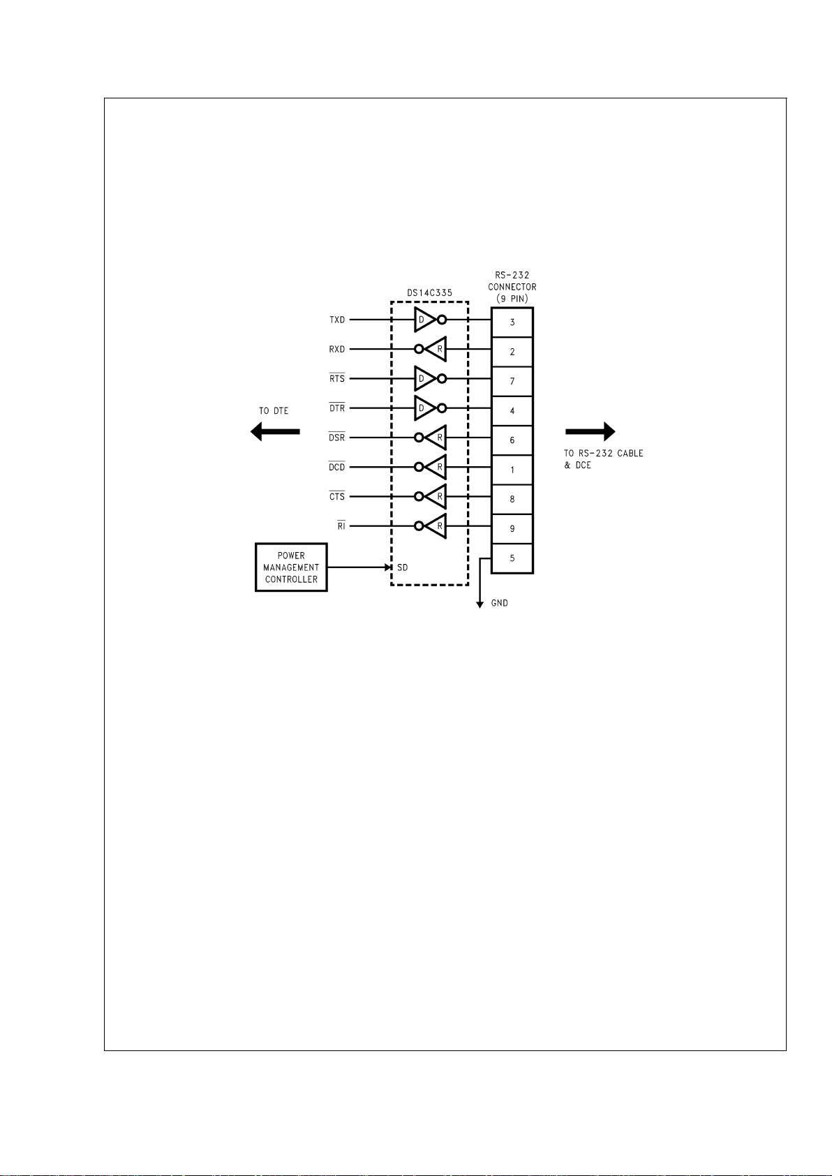
9-Pin SERIAL PORT APPLICATION
In a typical Data Terminal Equipment (DTE) to Data
Circuit-Terminating Equipment (DCE) 9-pin de-facto interface implementation, 2 data lines and 6 control lines are required. The data lines are TXD and RXD and the control
lines are RTS, DTR, DSR, DCD, CTS and RI. The
DS14C335 is a 3 x 5 Driver/Receiver and offersa single chip
solution for the DTE interface as shown in
Figure 9
.
Ring Indicator (RI) is used to inform the DTE that an incoming call is coming from a remote DCE. When the DS14C335
is in SHUTDOWN (SD) mode, receiver five (R5) remains active and monitors RI circuit. This active receiver (R5) alerts
the DTE to switch the DS14C335 from SHUTDOWN to active mode.
MOUSE DRIVING
The DS14C335 was tested for drive current under the following mouse driving conditions:
•
Two driver outputs set at VOHand their outputs were tied
together (paralleled), sourcing current to supply the V+
terminal of the mouse electronics
•
One driver output set at VOLto sink the current from the
V− terminal of the mouse electronics
•
One receiver was used to accept data from the mouse
•
Power Supply Voltage (VCC): 3.0V to 3.6V
Completion of the testing (performed by National’s Data
Transmission Applications Group and a major PC manufacturer) concluded that the DS14C335 and it’s DC-DC Convertor supplied adequate drive capability to power a typical PC
mouse. The mouse tested was specified with the following
conditions:
10 mA at +6V
5.0 mA at −6V
Since driver current is limited, it is recommended that newer
lower power mice be specified for battery powered applications. Using older high power mice is wasteful of precious
battery charge.
EXTERNAL DC-DC CONVERTOR COMPONENTS
The DS14C335 with it’s unique DC-DC Convertor triples the
power supply voltage (3.0V) to +9.3V and then inverts it to a
−9V potential. This unique convertor ONLY requires 5 external surface mount 0.47 µF capacitors. The five identical
components were chosen to simplify PCB layout and the
procurement of components. The DS14C335’s DC-DC Convertor also provides a larger signal swing (higher at RS-232
standard data rates) which translates to more noise margin
for the rejection of ground potential differences, induced
noise, and crosstalk compared to other DC-DC convertor
schemes which only provide limited signal swing and limited
noise margin.
DC-DC CONVERTOR CAPACITORS
The use of polarized capacitors is not required. However, if
they are used, the polarity indicated in the DS14C335 Functional Diagram must be honored for proper operation. Surface mount capacitors or ceramic capacitors may be used,
however, for optimal efficiency, capacitors with a low effective series resistance (ESR) should be used. Values in the
low Ohms(Ω) is normally acceptable.
INTEROPERATION WITH +5V UARTs
The DS14C335 provides full RS-232 driver output levels and
a single chip solution for the popular 9-pin defacto serial port.
This device may be used in either pure +3V applications or
DS011734-11
FIGURE 9. Typical DTE Application
DS14C335
www.national.com 6

Application Information (Continued)
mixed power supplied +3V/+5V applications. The Driver Input (DIN) and ShutDown (SD) input pins can directly accept
full +5V levels without the need for any external components.
The Receiver Output (ROUT) is specified at 2.4V minimum
while sourcing 1 mA. This level is compatible with standard
TTL thresholds. For a complete discussion on “Interoperation of the DS14C335 with +5V UARTs” please see National
Application Note AN-876.
POWER DISSIPATION IN REAL RS-232 APPLICATIONS
The DS14C335 DC-DC Convertor uses special circuitry that
helps limit the increase in power supply current as frequency
increases. A complete description of power dissipation and
calculations for RS-232 applications can be found in National Application Note AN-914 titled “Understanding Power
Requirements in RS-232 Applications”. Typical performance
curves are also located in this datasheet for quick reference.
Typical Performance Characteristics
Supply Current vs Frequency
vs Driver Loads
DS011734-12
Supply Current vs Frequency
vs Driver Loads
DS011734-13
Supply Power vs Data Rate
DS011734-14
Supply Current vs
Frequency (Receiver)
DS011734-15
DS14C335
www.national.com7

Typical Performance Characteristics (Continued)
Driver Output vs Data Rate
DS011734-16
DS14C335
www.national.com 8
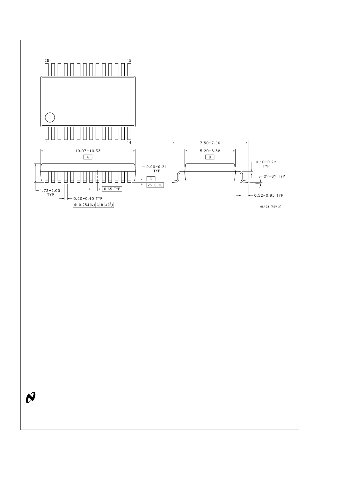
Physical Dimensions inches (millimeters) unless otherwise noted
LIFE SUPPORT POLICY
NATIONAL’S PRODUCTS ARE NOT AUTHORIZED FOR USE AS CRITICAL COMPONENTS IN LIFE SUPPORT
DEVICES OR SYSTEMS WITHOUT THE EXPRESS WRITTEN APPROVAL OF THE PRESIDENT AND GENERAL
COUNSEL OF NATIONAL SEMICONDUCTOR CORPORATION. As used herein:
1. Life support devices or systems are devices or
systems which, (a) are intended for surgical implant
into the body, or (b) support or sustain life, and
whose failure to perform when properly used in
accordance with instructions for use provided in the
labeling, can be reasonably expected to result in a
significant injury to the user.
2. A critical component is any component of a life
support device or system whose failure to perform
can be reasonably expected to cause the failure of
the life support device or system, or to affect its
safety or effectiveness.
National Semiconductor
Corporation
Americas
Tel: 1-800-272-9959
Fax: 1-800-737-7018
Email: support@nsc.com
National Semiconductor
Europe
Fax: +49 (0) 180-530 85 86
Email: europe.support@nsc.com
Deutsch Tel: +49 (0) 69 9508 6208
English Tel: +44 (0) 870 24 0 2171
Français Tel: +33 (0) 1 41 91 8790
National Semiconductor
Asia Pacific Customer
Response Group
Tel: 65-2544466
Fax: 65-2504466
Email: ap.support@nsc.com
National Semiconductor
Japan Ltd.
Tel: 81-3-5639-7560
Fax: 81-3-5639-7507
www.national.com
Order Number DS14C335MSA
NS Package Number MSA28
DS14C335 +3.3V Supply TIA/EIA-2323x5Driver/Receiver
National does not assume any responsibility for use of any circuitry described, no circuit patent licenses are implied and National reserves the right at any time without notice to change said circuitry and specifications.
 Loading...